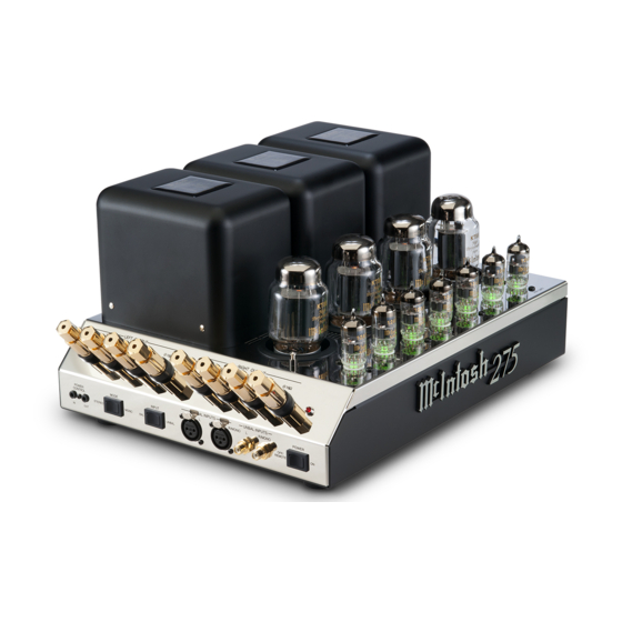
McIntosh MC275 Service Manual
Hide thumbs
Also See for MC275:
- Owner's manual (16 pages) ,
- Service manual (13 pages) ,
- Maintenance manual (4 pages)
Advertisement
Quick Links
Performance Specifications ..........................................2
Notes ...........................................................................2
Section Location ..........................................................3
Block Diagram .......................................................5 - 6
Interconnection Diagram ........................................7 - 8
Main Schematic and PCB .....................................9 - 16
Terminal Schematic ...................................................14
Terminal PCB......................................................17 - 18
SERVICE MANUAL
MC275
POWER AMPLIFIER
SERIAL NO. ABP1001 And Above
CONTENTS
Handcrafted in USA with US
and Imported Parts
Amplifier Schematic ...........................................19 - 20
Balanced Input / Unbalanced Input /
Power Control / Tube Light Schematic .................21 - 22
Amplifier / Balanced Input / Unbalanced Input /
Power Control / Tube Light PCB ..........................23 - 24
Parts List .............................................................25 - 29
Repacking Instruction ................................................31
MC275
Advertisement

Summary of Contents for McIntosh MC275
-
Page 1: Table Of Contents
MC275 MC275 POWER AMPLIFIER SERIAL NO. ABP1001 And Above Handcrafted in USA with US and Imported Parts CONTENTS Performance Specifications ..........2 Amplifier Schematic ...........19 - 20 Notes ................2 Balanced Input / Unbalanced Input / Section Location ............3 Power Control / Tube Light Schematic ....21 - 22 Block Diagram ............5 - 6... -
Page 2: Performance Specifications
240V ~ 50/60Hz at 1.8 Amps 250 milliwatts to rated power, 20Hz to 20,000Hz Standby: Less than 0.3 watts Note: Refer to the right side panel of the MC275 for the cor- Frequency Response rect voltage. +0, -0.5dB from 20Hz to 20,000Hz Overall Dimensions +0, -3.0dB from 10Hz to 100,000Hz... -
Page 3: Section Location
MC275 SECTION LOCATIONS... - Page 4 NOTES...
-
Page 5: Block Diagram
MC275 BLOCK DIAGRAM 12AX7A L OUTPUT 12AX7A 12AT7 L BALANCED BALANCED INPUT BUFFER 12AX7A 12AT7 PHASE BUFFER INVERTER L UNBALANCED INPUT MODE SWITCH SWITCH R/MONO UNBALANCED AUDIO DETECTOR R OUTPUT 12AX7A 12AX7A 12AT7 INPUT R/MONO BALANCED BALANCED BUFFER 12AX7A 12AT7... - Page 6 INPUT MAIN INPUT TERMINAL WHT/YEL WHT/YEL RIGHT LEFT MC275 TRANSFORMER WIRING AND FUSE REPLACEMENT (CONTACT MCINTOSH FOR CORRECT TRANSFORMER P/N) Voltage BLK BLK/GRY GRY VIO WHT/VIO BRN 1 BRN 2 Jumper Location (JMP1) Main Fuse (F1) T6.3AL250V T5AL250V T5AL250V T3.15AL250V INPUT T3.15AL250V...
- Page 7 MC275 MAIN 751376 SCH 1 of 3 +12V J1:1 VOUT J1:4 350mA 220µF 100V 110V JMP1 120V J1:7 PRIMARY J1:10 +12.6V J2:1 +700V J2:4 220V 230V 240V J2:7 2.2k +480V +350V J2:10 46.4k +12V 6-32 J5:2 TEST ONLY 680µF 47µF...
- Page 8 MAIN 751376 SCH 2 of 3 POWER UP TURN ON UNBAL DELAY CONTROL INP SW J26:2 J30:5 INPUT AUTO OFF J30:6 DISABLED AUTO OFF TIM ER INDICATOR 2.21M PC GND J26:1 47.5 47.5 J30:8 J30:9 PC ON TUBE LT J30:3 .1µF MONO 100K...
- Page 9 MC275 MAIN TERMINAL 751376 SCH 3 of 3 751379 SCH V9 PLT J32:6 L AUDIO TRANSFORMER V8 CATH J32:10 V8:1 KT88 V8 GRID J32:9 220 5W L OUT 16 FIL C J32:13 L 16(+) FIL C 1µF 2200pF KT88 FIL A...
- Page 10 MAIN 751376 PCB...
-
Page 11: Terminal Pcb
MC275 TERMINAL 751379 PCB... - Page 12 AMPLIFIER 751377 SCH 1µF V9 PLT J5:6 +350V +700V 200V .047µF V8 CATH J5:10 V8 CATH L BAL+ 22.1k J1:2 L BAL+ V1:1 L OUT 16 12AT7A .047µF L BAL- 100k 3.32K 100k V8 GRID L BAL- J5:9 J1:1 V2:1 12AT7A 100pF V3:2...
- Page 13 MC275 BAL INPUT UNBAL INPUT PWR CNTRL TUBE LT 751377 SCH 751377 SCH 751377 SCH 751377 SCH PC IN J8:1 PC IN J13:12 PC GND J13:4 J13:5 TUBE LT J13:10 Power Control J13:7 J13:8 LEFT INPUT RIGHT PC OUT J13:1...
- Page 14 BAL INP UNBAL INP PWR CTRL TUBE LT 751377 PCB 751377 PCB 751377 PCB 751377 PCB 751377 PCB...
-
Page 15: Parts List
PARTS LIST INTERCONNECT Ref. No. Description Part No. Ref. No. Description Part No. CAP ELECT 47UF 450V 066560 MCINTOSH BINDING POST 084226 CAP .47UF 50V 20% SMD0805 061373 MCINTOSH BINDING POST 084226 CAP .47UF 50V 20% SMD0805 061373 MCINTOSH BINDING POST 084226 CAP .47UF 50V 20% SMD0805... - Page 16 PARTS LIST (Cont’d.) MAIN PCB 751376 (Cont’d.) Ref. No. Description Part No. Ref. No. Description Part No. DIODE SMALL SIGNAL 4148 SMD 070199 PCB1 PC BD MAIN 130138 DIODE SMALL SIGNAL 4148 SMD 070199 TRANSISTOR NPN NPN A05 SMD 132333 DIODE SMALL SIGNAL 4148 SMD 070199 TRANSISTOR PNP A55 SMD...
- Page 17 MC275 PARTS LIST (Cont’d.) MAIN PCB 751376 (Cont’d.) Ref. No. Description Part No. Ref. No. Description Part No. IC SINGLE 2-INPUT NOR GATE SMD 133500 RES SMD0805 2.21K 1/8W 1% 145024 IC SINGLE 2 INPUT OR GATE SMD 133700 RES SMD0805 100K 1/8W 1%...
- Page 18 PARTS LIST (Cont’d.) AMP PCB 751377 (Cont’d.) Ref. No. Description Part No. Ref. No. Description Part No. CAP ELECT 4.7UF 50V 066512 CONN 12 PIN FFC SMD 118001 CAP ELECT 4.7UF 50V 066512 7 PIN SHROUDED HEADER 117910 DIODE ZENER 200V 1.5W 070177 RELAY DPDT SIGNAL 12V SMD 087084...
- Page 19 MC275 PARTS LIST (Cont’d.) AMP PCB 751377 (Cont’d.) Ref. No. Description Part No. Ref. No. Description Part No. RES MF 100K 1% 1/4W 144528 RES SMD0805 681 1/8W 1% 145002 RES SMD0805 475 1/8W 1% 145020 RES MF 100K 1% 1/4W 144528 RES SMD0805 3.32K 1/8W 1%...
- Page 20 NOTES...
-
Page 21: Repacking Instruction
If a shipping carton or any of the interior 400131 10-32 x 1/2 inch screw part(s) are needed, please call or write Customer 163073 Feet Service Department of McIntosh Laboratory. Please see the Part List for the correct part num- bers. TUBE COVER FOAM PAD WITH TUBE... - Page 22 The continuous improvement of its products is the policy of McIntosh Laboratory Incorporated, who reserve the right to improve design without notice. Because of the constant upgrading of McIntosh products’ circuitry and components, the Company cannot insure, and does not warrant, the accuracy of the within schematic material, which is intended for information only.


Need help?
Do you have a question about the MC275 and is the answer not in the manual?
Questions and answers