Advertisement
Analog Technologies
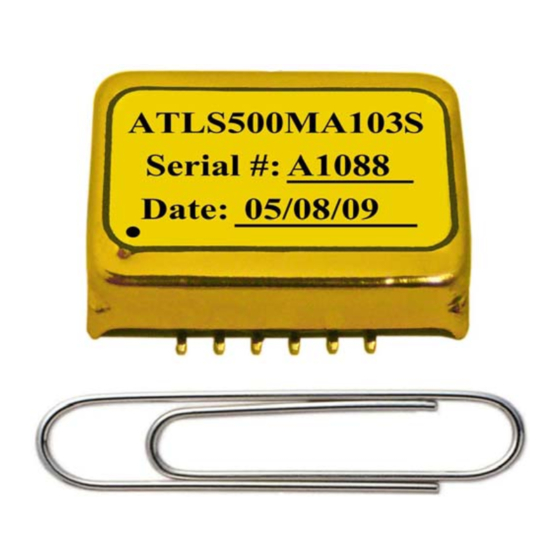
Figure 1. Physical Photo of ATLS500MA103S
FEATURES
Ultra Low Noise: <5μA*
High Current without Heat Sink: 500mA
High Absolute Accuracy: <0.1%
High Stability: <100ppm/°C
Dual Modulation Ports: High and Low Speed
Complete Shielding
Compact Size
100 % Lead (Pb)-free and RoHS Compliant
DIP and SMT Packages Available
*Total RMS between 0.1Hz to 0.5MHz.
APPLICATIONS
Driving laser diodes with low noise, including DPSSL,
EDFA, SOA, fiber laser, direct diode lasers, etc.
DESCRIPTION
The is an electronic module designed for driving diode
lasers with up to 500mA low noise current. Figure 1 shows
physical photo of .The output voltage is 1.5V to 4V when
powered by a 5V power supply.
When the maximum power consumed by the controller is
maintained to <1W, it does not require a heat sink to operate.
Table 1. Pin Function Descriptions
Pin #
Pin Name
Pin Type
1
SDN
Digital input
2
GND
Signal ground
2352 Walsh Ave. Santa Clara, CA 95051. U. S. A. Tel.: (408) 748-9100, Fax: (408) 748-9111
Copyrights 2000-2015, Analog Technologies, Inc. All Rights Reserved. Updated on 8/10/2015
Low Noise Constant Current Laser Controller
The controller has temperature compensation network so that
the output current maintains the same even as the controller
temperature rises.
In case the controller temperature exceeds a preset limit, 120°C,
the controller will be shut down by itself to prevent the
controller from being damaged by the over heat.
The output current of the can be set by an input voltage
linearly or modulated by an external signal of up to 2MHz in
bandwidth, resulting in a minimum 1μS rise and fall times at
the output current.
A highly stable low noise 2.5V reference voltage is provided
internally for setting the output current. This reference can also
be used as the voltage reference for external ADCs (Analog to
Digital Converters) and/or DACs (Digital to Analog
Converters) which are utilized for converting the analog signals,
such as LIO which represents the output current, into digital
signals, and/or converting the digital signals into analog ones
for setting the analog voltages, such as LIS which sets the
output current.
The is packaged in a 6 sided metal enclosure, which blocks
EMIs (Electro-Magnetic Interferences) to prevent the controller
and other electronics from interfering each other.
There are 2 packaging versions available: DIP through hole
package and surface mount type.
Warning
Figure 2 is the actual size top view of the , which shows the pin
names and locations. Its thickness is 5mm. Table 1 shows the
pin function descriptions.
For ATLS500mA103: Shut down control. Negative logic.
For ATLS500mA103-PD: Shut down control. Positive logic. There is a pull-down
resistor of 100K to the ground.
Signal ground pin. Connect ADC and DAC grounds to here.
ATLS500MA103
: Both the surface mount and the through hole
types of modules can only be soldered manually
on the board by a solder iron of < 310ºC (590ºF),
not go through a reflow oven process.
1
12
SDN
VPS
2
11
PGND
GND
2.5VR
3
10
LDC
LILM
4
9
LDA
LIS
5
8
TMPO
6
7
LPGD
LIO
14.5
Figure 2. Pin Names and Locations
Description
www.analogtechnologies.com
www.analogti.com
20
1
Advertisement
Table of Contents

Related Manuals for Analog Technologies ATLS500MA103


Summary of Contents for Analog Technologies ATLS500MA103
- Page 1 Pin Type Description For ATLS500mA103: Shut down control. Negative logic. Digital input For ATLS500mA103-PD: Shut down control. Positive logic. There is a pull-down resistor of 100K to the ground. Signal ground Signal ground pin. Connect ADC and DAC grounds to here.
-
Page 2: Specifications
Resistor R1 and capacitor C1 form a low pass filter, to lower the noise from the voltage reference. 2352 Walsh Ave. Santa Clara, CA 95051. U. S. A. Tel.: (408) 748-9100, Fax: (408) 748-9111 www.analogtechnologies.com Copyrights 2000-2015, Analog Technologies, Inc. All Rights Reserved. Updated on 8/10/2015 www.analogti.com... - Page 3 If not using a switch (S1) to control the laser, leave the To turn on: For ATLS500MA103, turn on the power by SDN pin unconnected. D2 is an LED, indicating when the...
- Page 4 Figure 6. Relationship between VPS and LDA LIO (V) = I_out × 5(V). 2352 Walsh Ave. Santa Clara, CA 95051. U. S. A. Tel.: (408) 748-9100, Fax: (408) 748-9111 www.analogtechnologies.com Copyrights 2000-2015, Analog Technologies, Inc. All Rights Reserved. Updated on 8/10/2015 www.analogti.com...
- Page 5 TMPO voltage to below 0.4V, the laser controller will be shut down. 2352 Walsh Ave. Santa Clara, CA 95051. U. S. A. Tel.: (408) 748-9100, Fax: (408) 748-9111 www.analogtechnologies.com Copyrights 2000-2015, Analog Technologies, Inc. All Rights Reserved. Updated on 8/10/2015 www.analogti.com...
-
Page 6: Mechanical Dimensions And Mounting
Figure 10. Dimensions of the SMT Package Controller Figure 11. Top Side PCB Foot-print for the DIP Package 2352 Walsh Ave. Santa Clara, CA 95051. U. S. A. Tel.: (408) 748-9100, Fax: (408) 748-9111 www.analogtechnologies.com Copyrights 2000-2015, Analog Technologies, Inc. All Rights Reserved. Updated on 8/10/2015 www.analogti.com... - Page 7 Figure 12. Top View of the Bottom Side PCB Foot-print Figure 13. Controller Internal Temperature vs. TMPO Voltage 2352 Walsh Ave. Santa Clara, CA 95051. U. S. A. Tel.: (408) 748-9100, Fax: (408) 748-9111 www.analogtechnologies.com Copyrights 2000-2015, Analog Technologies, Inc. All Rights Reserved. Updated on 8/10/2015 www.analogti.com...
-
Page 8: Ordering Information
ATI for its products and/or projects. 2352 Walsh Ave. Santa Clara, CA 95051. U. S. A. Tel.: (408) 748-9100, Fax: (408) 748-9111 www.analogtechnologies.com Copyrights 2000-2015, Analog Technologies, Inc. All Rights Reserved. Updated on 8/10/2015 www.analogti.com...
Need help?
Do you have a question about the ATLS500MA103 and is the answer not in the manual?
Questions and answers