
Related Manuals for Fastrax IT321

Summary of Contents for Fastrax IT321
- Page 1 REV 1.2 TECHNICAL DESCRIPTION Fastrax IT321 OEM GPS Receiver This document describes the electrical connectivity and main functionality of the Fastrax IT321 OEM GPS Receiver. November 19, 2007 Fastrax Ltd.
- Page 2 2007-11-19 Page 2 of 35 IT321_Tech_doc_12 TRADEMARKS Fastrax® is trademark of Fastrax Ltd. SiRF®, SiRFStar , TricklePower , Push-to-Fix , SiRFDrive are registered trademark and trademarks of SiRF Technology, Inc. All other trademarks are trademarks or registered trademarks of their respective...
- Page 3 Rev. Notes Date Initial documentation 2007-08-24 Module name change to IT321, abs. max power 2007-10-11 dissipation 300mW, oper. temp. range -30C… +85C, GPIO6 & 13 added to HW rev. B, added VDD ripple specification, added ON_OFF tim- ing, removed solder profile picture, added tape and reel spec, changed Application Board documents to rev C.
-
Page 4: Table Of Contents
2007-11-19 Page 4 of 35 IT321_Tech_doc_12 CONTENTS GENERAL DESCRIPTION ................7 Block diagram ..................8 Frequency Plan ..................8 SPECIFICATIONS................... 9 General ....................9 Absolute maximum ratings..............10 OPERATION ....................11 Operating modes................11 Normal mode ..................11 3.2.1 Output configuration ..............11 3.2.2 Power management system modes ......... - Page 5 Tape and reel ..................24 REFERENCE DESIGN .................. 26 Reference circuit diagram ..............26 PCB layout issues ................27 IT321 APPLICATION BOARD............... 29 Card Terminal I/O-connector ............. 29 Bill of materials, PCB rev C ............... 31 Circuit drawing, rev C ................ 32 Assembly drawing, Top side, rev C ..........
- Page 6 2007-11-19 Page 6 of 35 IT321_Tech_doc_12 COMPLEMENTARY READING The following Fastrax reference documents are complementary reading for this document. All operating and firmware related documentation is also available at www.fastrax.fi Ref. # File name Document name The following SiRF reference documents are also complementary reading for this document.
-
Page 7: General Description
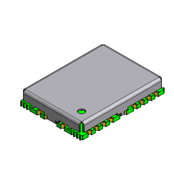
Page 7 of 35 IT321_Tech_doc_12 GENERAL DESCRIPTION The Fastrax IT321 is an OEM GPS receiver module, which provides the SiRFstarIII receiver (ref I) functionality using the state of the art SiRF GSC3LT chip. The module has tiny form factor 10.4x14.0mm, height is 2.3mm nominal (2.6mm max). -
Page 8: Block Diagram
TCXO CTRL_TCXO Figure 1 Block diagram 1.2 Frequency Plan Clock frequencies generated internally at the Fastrax IT321 receiver: • 32768 Hz real time clock (RTC) • 16.369 MHz master clock (TCXO) • 1571.424 MHz local oscillator of the RF down-converter... -
Page 9: Specifications
2007-11-19 Page 9 of 35 IT321_Tech_doc_12 SPECIFICATIONS 2.1 General General Specifications Table 1 Receiver GPS L1 C/A-code, SPS Chip set & Navigation sensitivity SiRF GSC3LT -159dBm Channels 20 physical (12 in tracking, firmware limited) Update rate 1 Hz default (fix rate configurable with SiRF TricklePower) Supply voltage, VDD +3.25V…+5.5 V (can be raw battery supply) -
Page 10: Absolute Maximum Ratings
2007-11-19 Page 10 of 35 IT321_Tech_doc_12 Note 1: Operation in the storage temperature range –40°C… +85°C is allowed but Time-to-First-Fix and other GPS performance may be de- graded. 2.2 Absolute maximum ratings Table 2 Absolute maximum ratings Item unit Operating and storage temperature ºC Power dissipation Supply voltage, VDD... -
Page 11: Operation
IT321_Tech_doc_12 OPERATION 3.1 Operating modes After power up the IT321 module (with Flash version) boots from the internal ROM or from flash memory depending on the BOOT1 and BOOT2 control inputs (see Table 4). With ROM code version the BOOT1 & 2 inputs can be left uncon- nected but the inputs GPIO6 &... -
Page 12: Power Management System Modes
Disabled Enabled Enabled Ephemeris 3.2.2 Power management system modes The IT321 module supports also SiRF operating modes for reduced average power consumption (ref III) like Adaptive TricklePower Push-to-Fix modes: 1. Adaptive TricklePower: In this mode the receiver stays at Full Power for 200…... -
Page 13: Hibernate Mode
2007-11-19 Page 13 of 35 IT321_Tech_doc_12 SiRF binary protocol message ID151 (ref III). The receiver stays once in while in Full Power automatically to collect new ephemeris and almanac data from rising satellites. 2. Push-to-Fix: In this mode the receiver is configured to wake up periodically, typically every 1800 sec, to collect new ephemeris data from rising satellites. -
Page 14: Procedure For Re-Programming The Flash Firmware
1. Connect UART (RXA and TXA signals) to PC via RS232 converter. 2. Set the module to UART boot mode: Power up the module to Flash programming mode according to Table 4. when using Fastrax Evaluation kit power up the kit and toggle Prog/Reset switch to Prog position. - Page 15 2007-11-19 Page 15 of 35 IT321_Tech_doc_12 Figure 2 SiRFFlash utility settings...
-
Page 16: Connectivity
2007-11-19 Page 16 of 35 IT321_Tech_doc_12 CONNECTIVITY 4.1 Connection assignments The I/O connections are available as soldering pads on the bottom side of the module. These pads are also used to attach the module on the motherboard in application. All unconnected I/O should be left open (floating) unless instructed to use pull external up or pull down. - Page 17 2007-11-19 Page 17 of 35 IT321_Tech_doc_12 Ground TSYNC GPIO8 Option for Timing pulse input in A- GPS version. Pull low when not used with e.g. 10kohm. VCC=1.8V. GPIO2 Control input for protocol configura- tion. VCC=1.8V. For default pull low. Ground GPIO1 Valid fix indicator output.
-
Page 18: Power Supply
IT321_Tech_doc_12 4.2 Power supply The IT321 module requires only one power supply VDD, which can be supplied directly from a battery since the module has internal regula- tors. Keep the supply active all the time in order to keep the non- volatile RTC &... -
Page 19: On_Off Control Input
2007-11-19 Page 19 of 35 IT321_Tech_doc_12 NOTE With ROM code version the BOOT inputs can left unconnected (floating) since internal pull ups are configured to ROM mode as de- fault. NOTE With embedded flash version the BOOT1 and BOOT2 input can be connected to the same boot control source from host. -
Page 20: Antenna Input
2007-11-19 Page 20 of 35 IT321_Tech_doc_12 Figure 3 Suggested ON_OFF Hibernate control timing diagram. NOTE If not used, pull ON_OFF signal to low state with e.g. 10kohm pull down resistor. If used, note that the input is CMOS 1.2V compatible. Use e.g. a resistive divider to reduce input voltage to 1.2V when using 1.8V or 3.3V host control source. -
Page 21: Active Gps Antenna
2007-11-19 Page 21 of 35 IT321_Tech_doc_12 4.6.1 Active GPS antenna The customer may use an external active GPS antenna for e.g. in mobile or indoor usage. It is suggested the active antenna has a net gain including cable loss in the range from +10 dB to +25 dB. NOTE Max antenna bias current is 15mA. -
Page 22: Gpio1 Valid Fix Indicator
2007-11-19 Page 22 of 35 IT321_Tech_doc_12 NOTE Pull ECLK signal to low state e.g. with 10kohm resistor. 4.9.1 GPIO1 Valid fix indicator GPIO1 is available as a valid fix indicator. Prior navigation the output stays at high state. During valid fix the output sends 100ms high state pulses at 1Hz rate. -
Page 23: Suggested Pad Layout And Pin Out
2007-11-19 Page 23 of 35 IT321_Tech_doc_12 I/O pad numbering and dimensions, bottom view. Figure 5 4.11 Suggested pad layout and pin out Figure 6 Suggested pad layout, occupied area and pin out, top view. -
Page 24: Manufacturing
Absolute max reflow temperature is 260C for ten seconds. 5.3 Moisture sensitivity Note that the IT321 is moisture sensitive at MSL 3 (see the standard IPC/JEDEC J-STD-020C). The module must be stored in the original moisture barrier bag or if the bag is opened, the module must be re- packed or stored in a dry cabin (according to the standard IPC/JEDEC J-STD-033B). - Page 25 2007-11-19 Page 25 of 35 IT321_Tech_doc_12 Figure 7 Tape and reel specification...
-
Page 26: Reference Design
Serial port TXA is connected to host UART input. RXA connection to host UART output is required when sending commands to IT321. Optional connectivity for host includes PPS signal for timing pur- poses, BOOT control inputs for e.g. re-programming the firmware with flash version and ON_OFF control input for Normal/Hibernate (ON/OFF) mode control. -
Page 27: Pcb Layout Issues
Figure 8 Reference Circuit Drawing 6.2 PCB layout issues The suggested 4-layer PCB build up is presented in the following ta- ble. Table 6 Suggested PCB build up Layer Description Signal + Ground with copper keep-out below IT321 Ground plane Signals... - Page 28 If possible, the amount of VIA holes underneath the module should be also minimized. For a multi-layer PCB the first inner layer below the IT321 is sug- gested to be dedicated for the ground plane. Below this ground layer other layers with signal traces are allowed.
-
Page 29: It321 Application Board
The Fastrax IT321 Application Board provides the IT321 connectivity to the Fastrax Evaluation Kit or to other evaluation purposes. It pro- vides a single PCB board equipped with the IT321 module, a control- lable switch for VDD supply, a 1.8V regulator, a 4 channel level trans- lator for 1.8V I/O to 3.3V conversion, an MCX antenna connector, and... - Page 30 UI indicator A output Ground Not connected Ground Not connected Ground TIMESYNC_1V8 GPIO8 Timesync timing input, VCC 1.8V Ground N_ON_OFF_1V8 Inverted ON_OFF control input, VCC 1V8 Ground ECLK_1V8 ECLK clock input, VCC 1.8V Alternative Interface to Fastrax Evaluation Signal name GPIO name...
-
Page 31: Bill Of Materials, Pcb Rev C
4,7uF 6,3V X5R 0805 +20% H3-4 FIDUCIAL FIDUCIAL, Circle, rectangle, triangle H1-2 HOLE HOLE 3.2mm IT321 IT321 MODULE 1x2P2.54 1x2 pin-header, straight, pitch 2.54mm 2x20 edge EDGE MOUNT SOCKET STRIP 40 PINS CON/MCX 50 Ohm male MCX connector PCB PCB1... -
Page 32: Circuit Drawing, Rev C
2007-11-19 Page 32 of 35 IT321_Tech_doc_12 7.3 Circuit drawing, rev C... -
Page 33: Assembly Drawing, Top Side, Rev C
2007-11-19 Page 33 of 35 IT321_Tech_doc_12 7.4 Assembly drawing, Top side, rev C 7.5 Artwork, layer 1 (Top), rev C... -
Page 34: Artwork, Layer 2, Rev C
2007-11-19 Page 34 of 35 IT321_Tech_doc_12 7.6 Artwork, layer 2, rev C 7.7 Artwork, layer 3, rev C... -
Page 35: Artwork, Layer 4 (Bottom), Rev C
2007-11-19 Page 35 of 35 IT321_Tech_doc_12 7.8 Artwork, layer 4 (Bottom), rev C...
Need help?
Do you have a question about the IT321 and is the answer not in the manual?
Questions and answers