Panasonic DMR-ES15EB Service Manual
Hide thumbs
Also See for DMR-ES15EB:
- Service manual (84 pages) ,
- Operating instructions manual (52 pages) ,
- Quick setup manual (2 pages)

Related Manuals for Panasonic DMR-ES15EB


Summary of Contents for Panasonic DMR-ES15EB
- Page 1 ORDER NO.DSD0602001CE DVD Recorder DMR-ES15EB DMR-ES15EP DMR-ES15EC DMR-ES15EG DMR-ES15EBL Vol. 1 Colour (S).......Silver Type (K).......Black Type (ES15EP/EC/EG) SPECIFICATIONS...
- Page 2 1. Safety Precaution 1.1. General guidelines 1. When servicing, observe the original lead dress. If a short circuit is found, replace all parts which have been overheated or damaged by the short circuit. 2. After servicing, see to it that all the protective devices such as insulation barriers, insulation papers shields are properly installed.
- Page 3 Figure 1 1.1.2. Leakage current hot check (See Figure 1 1. Plug the AC cord directly into the AC outlet. Do not use an isolation transformer for this check. 2. Connect a 1.5k , 10 watts resistor, in parallel with a 0.15 F capacitors, between each exposed metallic part on the set and a good earth ground such as a water pipe, as shown Figure...
- Page 4 1. Immediately before handling any semiconductor component or semiconductor-equipped assembly, drain off any ESD on your body by touching a known earth ground. Alternatively, obtain and wear a commercially available discharging ESD wrist strap, which should be removed for potential shock reasons prior to applying power to the unit under test.
- Page 5 2.3. Service caution based on legal restrictions 2.3.1. General description about Lead Free Solder (PbF) The lead free solder has been used in the mounting process of all electrical components on the printed circuit boards used for this equipment in considering the globally environmental conservation.
- Page 6 (Definition: The letter of “PbF” is printed on the PCB using the lead free solder.) To put lead free solder, it should be well molten and mixed with the original lead free solder. Remove the remaining lead free solder on the PCB cleanly for soldering of the new IC. Since the melting point of the lead free solder is higher than that of the normal lead solder, it takes the longer time to melt the lead free solder.
- Page 7 4. Specifications...
- Page 9 5. New Feature...
- Page 10 5.1. About DivX 5.1.1. General DivX is a new video compressing format that is applied MPEG4 technology to improve image quality and the compressibility, and it is developed by the DivXNetworks, Inc., Video file of high resolution and the high picture quality can be made though it is a high compressibility.
- Page 17 5.1.3. About DivX DRM Divx file includes file to which DRM(Digital Right Management) is applied and file not applied. This item is a content that relates only in treating file to which DRM is applied. 1. Registration Code display function 2.
- Page 18 1) Registration Code display function Registration Code is alphanumeric character sequence 8bytes inputted as recorder information, in case a use purchases or rent a DivX DRM file in a network. Registration code is a character sequence generated at random, and differs in each recorder. Moreover, Registration code is updated by new user authentication ever if same recorder.
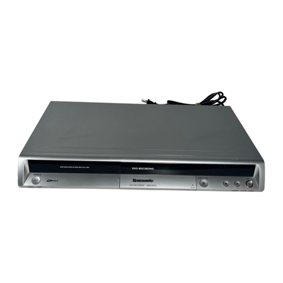
- Page 19 6. Location of Controls and Components Followings are the Location of Controls and Components for DMR-ES15EB as a sample. For other models, refer to each Operation Instructions.
- Page 21 7. Operation Instructions 7.1. Taking out the Disc from DVD-Drive Unit when the Disc cannot be ejected by OPEN/CLOSE button 7.1.1. Forcible Disc Eject 7.1.1.1. When the power can be turned off. 1. Turn off the power and press [STOP] [CH UP] keys on the front panel simultaneously for 5 seconds.
- Page 22 8. Service Mode 8.1. Self-Diagnosis and Special Mode Setting 8.1.1. Self-Diagnosis Functions Self-Diagnosis Function provides information for errors to service personnel by “Self- Diagnosis Display” when any error has occurred. U**, H** and F** are stored in memory and held. You can check latest error code by transmitting [0] [1] of Remote Controller in Service Mode.
- Page 23 Error Diagnosis contents Description Monitor Automatic FL display Code Display The unit is carrying No display out its recovery process. Hang-up Displayed when communication No display error has occurred between Main microprocessor and Timer microprocessor. Displayed is left until the [POWER] key is pressed.
- Page 24 Error Diagnosis contents Description Monitor Automatic FL display Code Display Restoration operation Since the power cord fell out No display PLEASE during a power failure or WAIT operation, it is under restoration operation. *It will OK, if a display disappears automatically.
- Page 25 Item FL display Key operation Mode name Description Front Key Forced disc eject Removing a disc that cannot be The display before When the power is off, ejected. execution leaves. press [STOP] and [CH UP] keys simultaneously for 5 The tray will open and unit will seconds.
- Page 26 Item FL display Key operation Mode name Description Front Key Aging Perform sequence of modes as * Display following the then When the power is ON, Aging Description shown below mode. press [STOP], [POWER] continually. and [OPEN/CLOSE] simultaneously for over 5 seconds and less than 10 seconds.
- Page 27 Item FL display Key operation Mode name Description Front Key Demonstration Ejection of the disc is prohibited. *When lock the tray. When the power is on, lock/unlock press [STOP] and The lock setting is effective until [POWER] keys unlocking the tray and not simultaneously for 5 released by “Main unit seconds.
- Page 28 Item FL display Key operation Mode name Description (Remote controller key) Release Items Item of Service Mode executing is Press [0] [0] or [Return] in cancelled. service mode. Error Code Display Last Error Code of U/H/F held by Press [0] [1] in service Timer is displayed on FL.
- Page 29 Item FL display Key operation Mode name Description (Remote controller key) RTSC Return in XP AV1 input signal is encoded (XP), Initial mode: EE2/ Interlace/ Press [1] [3] in service decoded (XP) and output XP/ Audio 48kHz mode. decoded signal to external (A &...
- Page 30 Item FL display Key operation Mode name Description (Remote controller key) Delete the Laser Laser used time stored in the Press [9] [5] in service Used Time memory of the unit is deleted. mode. RAM Drive Last RAM Drive error code display. 1.
- Page 31 Item FL display Key operation Mode name Description (Remote controller key) Laser power Drive state is judged based on confirmation difference between laser power into RAM Drive in service mode. value at shipping and present (Other media are assumed to be non- laser power value.
- Page 32 Item FL display Key operation Mode name Description (Remote controller key) Display the Error Display the Error History stored Display reason of error for Press [6] [5] in service History on the unit. 5 seconds. mode. Then press [0] [1] ~ [1] [9], the past 19 error histories are displayed.
- Page 33 Item FL display Key operation Mode name Description (Remote controller key) AV2(RGB)/AV1(V) I Set input to AV2 (RGB) and set Press [8] [3] in service /O Setting output to AV1 (V) for I/O checking mode. P50(H) Output Timer Microprocessor IC7501-76 When OK.
- Page 34 Part Number Description Compatibility RFKZ0365 Extension Cable (MainP.C.B. - Digital P.C.B. / 64 Pin) RFKZ0240 Extension Cable (MainP.C.B. - Power P.C.B. / 19 Pin) Same as E75V/ES30V Series JZS0484 Eject Pin Same as E50 Series RFKZ03D01K Lead Free Solder (0.3mm/100g Reel) RFKZ06D01K Lead Free Solder (0.6mm/100g Reel) RFKZ10D01...
- Page 35 10.3. Top Case 1. Remove 2 screws (A) and 3 screws (B). 2. Slide Top Case rearward and open the both ends at rear side of the Top Case a little and lift the Top Case in the direction of the arrows.
- Page 36 10.4. Front Panel 1. Unlock 6 tabs in (A) - (F) turn. Pull with the front panel in the direction of your side.
- Page 37 10.5. RAM/Digital P.C.B. Module 1. Remove 6 Screws (A). 2. Lift up Digital P.C.B. slightly so to disconnect Connectors to remove Digital P.C.B.
- Page 38 3. Put Digital P.C.B. on RAM Drive and remove RAM/Digital P.C.B. Module.
- Page 39 Note: RAM/Digital P.C.B. Module as service part has no heat sink unit. Before returning to customer, heat sink unit should be installed on Digital P.C.B..
- Page 41 10.6. DV Jack P.C.B. 1. Remove 1 Screw (A) to remove DV jack P.C.B. 10.7. Power P.C.B. 1. Remove 1 Screw (A).
- Page 42 2. Remove 3 Screws (B) and disconnect Connector (A). 3. Unlock Power P.C.B. from a Flange to remove Power P.C.B.
- Page 43 10.8. Rear Panel 1. Remove 7 Screws (A) and 1 Screw (B). 2. Unlock 2 Locking Tabs (A) to remove Rear Panel.
- Page 44 10.9. Main P.C.B. and Front (L) P.C.B. 1. Remove 8 Screws (A) and 1 Screw (B). 2. Remove Digital Angle to remove Main P.C.B. and Front (L) P.C.B..
- Page 45 10.10. Tuner P.C.B. 1. Pull out the Tuner P.C.B. in the direction of the arrow.
- Page 46 11. Measurements and Adjustments 11.1. Service Positions Note: For description of the disassembling procedure, see the section 10. 11.1.1. Checking and Repairing of Power P.C.B.
- Page 47 11.1.2. Checking and Repairing of RAM / Digital P.C.B. Module...
- Page 48 11.1.3. Checking and Repairing of Main P.C.B.
- Page 49 11.2. Caution for Replacing Parts 11.2.1. Items that should be done after replacing parts...
- Page 50 11.3. Standard Inspection Specifications after Making Repairs After making repairs, we recommend performing the following inspection, to check normal operation.
- Page 51 Turn on the power, and confirm items pointed out. Items pointed out should reappear. Insert RAM disc. The Panasonic RAM disc should be recognized. Enter the EE (TU IN / AV IN - AV OUT) mode. No abnormality should be seen in the picture, sound or operation.
-
Page 52: Table Of Contents
12.4. Analog Timer Block Diagram 13. Schematic Diagram 13.1. Interconnection Schematic Diagram 13.2. Power Supply Schematic Diagram 13.3. Main Net (1/4) Section (Main P.C.B. (1/4)) Schematic Diagram 13.4. Main Net (2/4) Section (Main P.C.B. (1/4)) Schematic Diagram 13.5. Main Net (3/4) Section (Main P.C.B. (1/4)) Schematic Diagram 13.6. - Page 53 13.7. A/V I/O (1/4) Section (Main P.C.B. (2/4)) Schematic Diagram (AV) 13.8. A/V I/O (2/4) Section (Main P.C.B. (2/4)) Schematic Diagram (AV) 13.9. A/V I/O (3/4) Section (Main P.C.B. (2/4)) Schematic Diagram (AV) 13.10. A/V I/O (4/4) Section (Main P.C.B. (2/4)) Schematic Diagram (AV) 13.11.
- Page 54 13.16. Tuner Pack Schematic Diagram 13.17. Front (L) Schematic Diagram 13.18. DV Jack Schematic Diagram 14. Printed Circuit Board 14.1. Power P.C.B. 14.2. Main P.C.B. 14.2.1. Main P.C.B. (1/4 Section) 14.2.2. Main P.C.B. (2/4 Section) 14.2.3. Main P.C.B. (3/4 Section) 14.2.4.
- Page 55 14.3. Tuner P.C.B. and DV Jack P.C.B. 14.4. Front (L) P.C.B. 15. Appendix for Schematic Diagram 15.1. Voltage and Waveform Chart Note) Circuit voltage and waveform described herein shall be regarded as reference information when probing defect point, because it may differ from an actual measuring value due to difference of Measuring instrument and its measuring condition and product itself.
- Page 56 INITIAL/LOGO ABBREVIATIONS A0~UP ADDRESS ACLK AUDIO CLOCK AD0~UP ADDRESS BUS ADATA AUDIO PES PACKET DATA ADDRESS LATCH ENABLE AMUTE AUDIO MUTE AREQ AUDIO PES PACKET REQUEST AUDIO RF SERVO AMP INVERTED INPUT SERVO AMP OUTPUT ASYNC AUDIO WORD DISTINCTION SYNC BIT CLOCK (PCM) BCKIN BIT CLOCK INPUT...
- Page 57 INITIAL/LOGO ABBREVIATIONS ERROR TORQUE CONTROL ERROR TORQUE CONTROL REFERENCE ENCODER SELECT ENCSEL EXTERNAL M CLOCK (81MHz/ ETMCLK 40.5MHz) ETSCLK EXTERNAL S CLOCK (54MHz) FBAL FOCUS BALANCE FCLK FRAME CLOCK FOCUS ERROR FOCUS ERROR AMP INVERTED INPUT FOCUS ERROR AMP OUTPUT FREQUENCY GENERATOR FREQUENCY SUB CARRIER FSCK...
- Page 58 INITIAL/LOGO ABBREVIATIONS READ ENABLE RFENV RF ENVELOPE RF PHASE DIFFERENCE OUTPUT (CD-ROM) REGISTER SELECT RSEL RF POLARITY SELECT RESET RESERVE SBI0, 1 SERIAL DATA INPUT SBO0 SERIAL DATA OUTPUT SBT0, 1 SERIAL CLOCK SERIAL DATA CLOCK SCKR AUDIO SERIAL CLOCK RECEIVER SERIAL CLOCK SCLK...
- Page 59 INITIAL/LOGO ABBREVIATIONS VBLANK V BLANKING COLLECTOR POWER SUPPLY VOLTAGE VCDCONT VIDEO CD CONTROL (TRACKING BALANCE) DRAIN POWER SUPPLY VOLTAGE VREF VIDEO FEED BACK VOLTAGE REFERENCE SOURCE POWER SUPPLY VOLTAGE WAIT BUS CYCLE WAIT WDCK WORD CLOCK WRITE ENABLE HIGH WORD SELECT RECEIVER X' TAL XALE X ADDRESS LATCH ENABLE...
- Page 60 16.2. Replacement Parts List Notes: *Important safety notice: Components identified by mark have special characteristics important for safety. Furthermore, special parts which have purposes of fire-retardant (resistors), high-quality sound (capacitors), low-noise (resistors), etc. are used. When replacing any of components, be sure to use only manufactures specified parts shown in the parts list.
- Page 61 Ref. No. Part No. Part Name & Description Remarks C1540 F1H1H1030006 50V 0.01U C3001 F1H1C104A042 16V 0.1U C3002 F1H1H1030006 50V 0.01U C3003 F1H1C104A042 16V 0.1U C3004 F1H1C104A042 16V 0.1U C3005 F2A0J471A016 6.3V 470U C3006 F2A0J471A016 6.3V 470U C3007 F2A1A4710038 10V 470U C3008 F2A1A1010072 10V 100U...
- Page 62 Ref. No. Part No. Part Name & Description Remarks C4023 F2A1H1R0A236 50V 1U C4024 F2A1E1010067 25V 100U C4025 F2A1H1R0A236 50V 1U C4027 F2A1H100A236 50V 10U C4028 F2A1H100A236 50V 10U C4033 F2A1C470A637 16V 47U C4034 F2A1C470A637 16V 47U C4055 F1H1C104A008 16V 0.1U C4056 F2A1C471A628 16V 470U...
- Page 63 Ref. No. Part No. Part Name & Description Remarks C7337 ECJ1VB1A474K 10V 0.47U EGK,EGS C7338 ECJ1VB1A474K 10V 0.47U EGK,EGS C7339 F1H1H9R0A735 50V 9P EGK,EGS C7340 F1H1C104A042 16V 0.1U C7401 F2A1C471A628 16V 470U C7402 F1H1H1030006 50V 0.01U C7404 ECJ1VB1A105K 10V 1U C7406 ECJ1VB1A105K 10V 1U...
- Page 64 Ref. No. Part No. Part Name & Description Remarks C7584 F4D55473A013 5.5V 0.047U C7592 F2A0J470A245 6.3V 47U D3901 MA2C165001VT DIODE D4001 MA2C165001VT DIODE D4005 MA3Z142D0LG DIODE D4006 MA3Z142D0LG DIODE D7403 MA2C165001VT DIODE D7501 B0BA03600021 DIODE D7502 B0ACCK000005 DIODE D7504 MAZ4220NLF DIODE D7505 B0AADM000003...
- Page 65 Ref. No. Part No. Part Name & Description Remarks K7308 D0YBR0000020 1/10W 0 K7501 D0YBR0000020 1/10W 0 K7502 D0YBR0000020 1/10W 0 K7506 D0YBR0000020 1/10W 0 K7507 D0YBR0000020 1/10W 0 K7508 D0YBR0000020 1/10W 0 L4901 G0C220KA0065 COIL 22UH L7303 G0C1R0JA0019 COIL 1UH EBS,EPK,EPS,EBLS,ECK,ECS L7304 G0C2R2JA0019...
- Page 66 Ref. No. Part No. Part Name & Description Remarks LB7516 D0YBR0000020 1/10W 0 LB7517 D0YBR0000020 1/10W 0 P1501 K1KA19A00007 CONNECTOR(19P) P7402 K1KY64A00001 CONNECTOR(64P) PP7401 K1KA18AA0288 CONNECTOR(18P) Q4006 2SD132800L TRANSISTOR Q4007 2SD132800L TRANSISTOR Q4008 2SD132800L TRANSISTOR Q4009 2SD132800L TRANSISTOR Q7401 2SD1819ARL TRANSISTOR Q7402 2SD1819A0L...
- Page 67 Ref. No. Part No. Part Name & Description Remarks R3925 D1BB75R0A010 2W 75 R3926 D1BB75R0A010 2W 75 R3927 D1BB75R0A010 2W 75 R3928 D0GB750JA057 1/10W 75 R3929 D0GB750JA057 1/10W 75 R3930 D0GB750JA057 1/10W 75 R3932 D0GB750JA057 1/10W 75 R3934 D0GB750JA057 1/10W 75 R3935 D0GB750JA057 1/10W 75...
- Page 68 Ref. No. Part No. Part Name & Description Remarks R7322 D0YBR0000020 1/10W 0 EBS,EPK,EPS,EBLS,ECK,ECS R7323 D0GB562JA057 1/10W 5.6K EGK,EGS R7324 D0GB221JA057 1/10W 220 R7325 D0GB221JA057 1/10W 220 R7326 D0GB122JA057 1/10W 1.2K EGK,EGS R7326 D0YBR0000020 1/10W 0 EBS,EPK,EPS,EBLS,ECK,ECS R7401 D0GB104JA057 1/10W 100K R7402 D0GB103JA057 1/10W 10K...
- Page 69 Ref. No. Part No. Part Name & Description Remarks R7572 D0GB101JA057 1/10W 100 R7576 D0GB102JA057 1/10W 1K R7577 D0GB103JA057 1/10W 10K R7579 D0GB223JA057 1/10W 22K R7582 D0GB104JA057 1/10W 100K R7583 D0GB472JA057 1/10W 4.7K R7584 D0GB473JA057 1/10W 47K R7585 D0GB225JA057 1/10W 2200K R7586 D0GB273JA057 1/10W 27K...
- Page 70 Ref. No. Part No. Part Name & Description Remarks W515 D0YBR0000020 1/10W 0 W516 D0YBR0000020 1/10W 0 W517 D0YBR0000020 1/10W 0 W518 D0YBR0000020 1/10W 0 W519 D0YBR0000020 1/10W 0 W520 D0YBR0000020 1/10W 0 W521 D0YBR0000020 1/10W 0 W522 D0YBR0000020 1/10W 0 W523 D0YBR0000020 1/10W 0...
- Page 71 R7812 ERJ6GEYJ681V 1/8W 680 EPK,EPS,EBLS Ref. No. Part No. Part Name & Description Remarks R7815 D0GB471JA057 1/10W 470 R7816 D0GB471JA057 1/10W 470 R7818 D0GB221JA057 1/10W 220 EPK,EPS,EBLS R7820 D0GB102JA057 1/10W 1K EPK,EPS,EBLS R7844 ERJ6GEYJ681V 1/8W 680 EPK,EPS,EBLS R7845 D0YBR0000020 1/10W 0 ECK,ECS R7846 D0GB562JA057...
- Page 72 Ref. No. Part No. Part Name & Description Remarks C1120 ECQU2A683MLC 100V 0.068U C1121 ECQU2A223MLC 100V 0.022U C1122 ECKWNA102MEV 250V 1000P C1123 ECKWNA102MEV 250V 1000P C1125 ECKWNA102MEV 250V 1000P C1143 F2B2W4700003 450V 47U C1150 EEUFM1V680B 35V 68U C1151 F1B3D102A011 2V 1000P C1152 ECJ2VC1H331J 50V 330P...
- Page 73 Ref. No. Part No. Part Name & Description Remarks R1158 ERX2SJR22E 2W 22 R1200 ERJ6GEYG152V 1/10W 1.5K R1201 ERJ6GEYG393V 1/8W 39K R1205 ERJ6GEYJ103V 1/8W 10K R1206 ERJ6GEYG242V 1/8W 2.4K R1207 ERJ6GEYJ103V 1/8W 10K R1208 ERJ6GEYJ222V 1/8W 2.2K R1209 ERJ6GEYJ102V 1/8W 1K R1210 ERJ6GEYJ102V 1/8W 1K...
- Page 74 Ref. No. Part No. Part Name & Description Remarks RHD30113-1K SCREW EPK,ECK,EGK RKM0552-S TOP CASE EBS,EPS,EBLS,ECS,EGS RKM0552-K TOP CASE EPK,ECK,EGK RMC0625 TUNER END XYN3+J8FJ SCREW RMQ1555 GASKET VEP71109A POWER SUPPLY P.C.B. (RTL) VEP07A91C TUNER P.C.B. (RTL)EBS VEP07A91D TUNER P.C.B. (RTL)EPK,EPS,EBLS VEP07A91B TUNER P.C.B.
- Page 75 2006 Matsushita Electric Industrial Co., Ltd. All rights reserved. Unauthorized copying and distribution is a violation of law.
-
Page 76: Schematic Diagram
THE CORRECT PART NUMBER IS SHOWN IN THE PARTS LIST,AND MAY BE K7403 VWJ0795=10 SLIGHTLYDIFFERNT OR AMENDED SINCE THIS DRAWING WAS PREPARED. C7439 Q7402 2SD1819A0L R7446 2000[D] UNREG_38V DMR-ES15EB/EP/EC/EG/EBL Main Net(2/4) Section MAIN NET SECTION (4/4) (Main P.C.B.(1/4)) Schematic Diagram(M) - Page 77 AV:A/V I/O Section:(Page: NOTE:DO NOT USE THE PART NUMBER SHOWN ON THIS DRAWING FOR ORDERRING. THE CORRECT PART NUMBER IS SHOWN IN THE PARTS LIST,AND MAY BE DMR-ES15EB/EP/EC/EG/EBL DE:Nicam Decoder Section:(Page: SLIGHTLYDIFFERNT OR AMENDED SINCE THIS DRAWING WAS PREPARED. Main Net(3/4) Section T:Timer Section:(Page: (Main P.C.B.(1/4))
- Page 78 K9ZZ00001279 (4/4) LOCATION MAP M:Main Net Section:(Page: AV:A/V I/O Section:(Page: DMR-ES15EB/EP/EC/EG/EBL DE:Nicam Decoder Section:(Page: NOTE:DO NOT USE THE PART NUMBER SHOWN ON THIS DRAWING FOR ORDERRING. Main Net(4/4) Section THE CORRECT PART NUMBER IS SHOWN IN THE PARTS LIST,AND MAY BE T:Timer Section:(Page: SLIGHTLYDIFFERNT OR AMENDED SINCE THIS DRAWING WAS PREPARED.
- Page 79 THE CORRECT PART NUMBER IS SHOWN IN THE PARTS LIST,AND MAY BE COMPONENTS IDENTIFIED WITH THE MARK HAVE THE SPECIAL CHARACTERISTICS FOR SAFETY. SLIGHTLY DIFFERNT OR AMENDED SINCE THIS DRAWING WAS PREPARED. WHEN REPLACING ANY OF THESE COMPONENTS.ONLY THE SAME TYPE. DMR-ES15EB/EP/EC/EG/EBL Power Supply Schematic Diagram...
- Page 80 ERJ3GEY0R00V C7520 C7534 0.01 NOTE:DO NOT USE THE PART NUMBER SHOWN ON THIS DRAWING FOR ORDERRING. DMR-ES15EB/EP/EC/EG/EBL TIMER SECTION THE CORRECT PART NUMBER IS SHOWN IN THE PARTS LIST,AND MAY BE (3/4) TIMER(1/4) Section SLIGHTLYDIFFERNT OR AMENDED SINCE THIS DRAWING WAS PREPARED.
- Page 81 C0EBE0000457 RESET R7620 IC-DETAIL BLOCK DIAGRAM C7581 K7509 0.01 VWJ0795 QR7506 D3R3V UNR521200L C7583 R7622 0.47 D7509 B0JDCE000002 X_SW_5R2V Vref R7623 R7621 100K C7584 F4D55473A013 DMR-ES15EB/EP/EC/EG/EBL M N O P Q TIMER SECTION TIMER(2/4) Section (4/4) (Main P.C.B.(4/4)) Schematic Diagram(T)
- Page 82 DE:Nicam Decoder Section:(Page: NOTE:DO NOT USE THE PART NUMBER SHOWN ON THIS DRAWING FOR ORDERRING. THE CORRECT PART NUMBER IS SHOWN IN THE PARTS LIST,AND MAY BE DMR-ES15EB/EP/EC/EG/EBL T:Timer Section:(Page: SLIGHTLYDIFFERNT OR AMENDED SINCE THIS DRAWING WAS PREPARED. TIMER(3/4) Section (Main P.C.B.(4/4))
- Page 83 R7642 5600 M:Main Net Section:(Page: AV:A/V I/O Section:(Page: DE:Nicam Decoder Section:(Page: DMR-ES15EB/EP/EC/EG/EBL T:Timer Section:(Page: NOTE:DO NOT USE THE PART NUMBER SHOWN ON THIS DRAWING FOR ORDERRING. TIMER(4/4) Section THE CORRECT PART NUMBER IS SHOWN IN THE PARTS LIST,AND MAY BE SLIGHTLYDIFFERNT OR AMENDED SINCE THIS DRAWING WAS PREPARED.
- Page 84 1000(EP/EBL) R7844 680(EP/EBL) NOTE:DO NOT USE THE PART NUMBER SHOWN ON THIS DRAWING FOR ORDERRING. DMR-ES15EB/EP/EC/EG/EBL THE CORRECT PART NUMBER IS SHOWN IN THE PARTS LIST,AND MAY BE SLIGHTLYDIFFERNT OR AMENDED SINCE THIS DRAWING WAS PREPARED. Tuner Pack Schematic Diagram...
-
Page 85: Interconnection Schematic Diagram
13 Schematic Diagram 13.1. Interconnection Schematic Diagram POWER P7001 P7505 P7401 P59001 XINTP DR12V KEY3 POWER KEY3 POWER SCLK DR12V XINTM DRGND SBPTM FRONT(L) P.C.B. DRGND SBMTP DR5V XMPREQ DR5V AU5V ITM2A XDMUTE ITA2M PP7401 PS7801 AADC L P OFF L2 BOOSTER5V BOOSTER 5V AADC R... - Page 86 DIGITAL P.C.B. COILU COILV COILW FP50004 OPEN SW PHOTO LED CARTRIGE REC INH P.C.B.Name Circuit Name Ref.No. Ref.No.50000 SERIES CLOSE SW Ref.No.50000,53000,54000,55000,57000 SERIES Digital Audio I/O Ref.No.54000 SERIES P.C.B. D Net Ref.No.59000 SERIES Model Select Ref.No.59000 SERIES DMR-ES15EB/EP/EC/EG/EBL Interconnection Schematic Diagram...
-
Page 87: Power Supply Schematic Diagram
13.2. Power Supply Schematic Diagram C1125 LB1122 LB1127 F1B2G1020002 VWJ0795=5 J0JHC0000048 ECKWNA102M ZA1103 ZA1104 D1140 EYF52BCY EYF52BCY B0EDKT000009 K3GE1ZA00010 K3GE1ZA00010 (S1WBA80-7062) L1120 L1121 G0B233D00001 G0B233D00001 C1121 F1101 ECQU2A223MLC T1150 K5D202BK0005 ETS28BF1Z6AD 250V T2AL P1101 K2AA2H000007 SEE THE SERVICE MANUAL LB1123 VWJ0795=5 LB1126 R1153... - Page 88 /VCC(STOP) PROTECTOR /VCC(STARTUP ON) IDP(LIMIIT/ BURST)SENS. ZERO CURRENT DET./ONDEAD TIMER CONTROL SOFT-DRIVE CIRCUIT CIRCUIT STANDBY CIRCUIT OCP THRESHOLD COMPARATOR/ RESTERT BURST MODE TIMER OCP THRESHOLD COMPARATOR ON WIDTH TIMER SOURCE /OCL HARACTERISTICS FOR SAFETY. YPE. DMR-ES15EB/EP/EC/EG/EBL Power Supply Schematic Diagram...
-
Page 89: Main Net (1/4) Section (Main P.c.b. (1/4)) Schematic Diagram (M)
13.3. Main Net (1/4) Section (Main P.C.B. (1/4)) Schematic Diagram (M) (1/4) LOCATION MAP X_SW_3R3V RESET_5R2V M:Main Net Section:(Page: AV:A/V I/O Section:(Page: DE:Nicam Decoder Section:(Page: T:Timer Section:(Page: NOTE:DO NOT USE THE PART NUMBER SHOWN ON THIS DRAWING FOR ORDERRING. THE CORRECT PART NUMBER IS SHOWN IN THE PARTS LIST,AND MAY BE SLIGHTLYDIFFERNT OR AMENDED SINCE THIS DRAWING WAS PREPARED. - Page 90 TUREG5V X_SW5R2V IC1510 C0CBCDG00006 (PG050DNA1ZPH) X_SW3R3 ANA5V ANA3R3V DMR-ES15EB/EP/EC/EG/EBL TION Main Net(1/4) Section (Main P.C.B.(1/4)) Schematic Diagram(M)
-
Page 91: Main Net (2/4) Section (Main P.c.b. (1/4)) Schematic Diagram (M)
13.4. Main Net (2/4) Section (Main P.C.B. (1/4)) Schematic Diagram (M) ZJ7402 K9ZZ00001279 QR7401 UNR521300L (UN5213-TX) IC7401 PS11R6V C0CBCYG000 (PQ200WNA1Z K7403 VWJ0795=10 C7439 R7446 2000[D] MAIN NET SECTION (4/4) - Page 92 NOTE:DO NOT USE THE PART NUMBER SHOWN ON THIS DRAWING FOR ORDERRING. THE CORRECT PART NUMBER IS SHOWN IN THE PARTS LIST,AND MAY BE 7403 SLIGHTLYDIFFERNT OR AMENDED SINCE THIS DRAWING WAS PREPARED. J0795=10 Q7402 2SD1819A0L R7446 2000[D] UNREG_38V DMR-ES15EB/EP/EC/EG/EBL Main Net(2/4) Section (Main P.C.B.(1/4)) Schematic Diagram(M)
-
Page 93: Main Net (3/4) Section (Main P.c.b. (1/4)) Schematic Diagram (M)
13.5. Main Net (3/4) Section (Main P.C.B. (1/4)) Schematic Diagram (M) MAIN NET SECTION (1/4) ANA5V P_OFF_L DR_P_ON_H ZJ7401 K9ZZ00001279 DR12V (M6520) IC1501 L1501 C0DAZJH00003 VWJ0795 ON[H] SENSE C1502 (3/4) LOCATION MAP NOTE:DO NOT USE THE PART NUMBER SHOWN ON THIS DRAWING FOR ORDERRING. THE CORRECT PART NUMBER IS SHOWN IN THE PARTS LIST,AND MAY BE SLIGHTLYDIFFERNT OR AMENDED SINCE THIS DRAWING WAS PREPARED. - Page 94 R7448 1800 DGND LB7417 J0JCC0000103 RPROUT_DM DGND LB7418 J0JCC0000103 GPYOUT_DM DGND LB7419 J0JCC0000103 BPBOUT_DM DGND 59 V_YIN_DM DGND CPNCIN_DM ZJ7406 K9ZZ00001279 M:Main Net Section:(Page: AV:A/V I/O Section:(Page: DMR-ES15EB/EP/EC/EG/EBL DE:Nicam Decoder Section:(Page: Main Net(3/4) Section T:Timer Section:(Page: (Main P.C.B.(1/4)) Schematic Diagram(M)
-
Page 95: Main Net (4/4) Section (Main P.c.b. (1/4)) Schematic Diagram (M)
13.6. Main Net (4/4) Section (Main P.C.B. (1/4)) Schematic Diagram (M) MAIN NET SECTION (2/4) R7405 Q7401 ERDS2TJ471T 2SD1819AWL R7404 D7403 MA2C165001VT (MA165TA5VT) L7402 G0A220GA0026 R7406 470K LB7407 J0JKB0000012 QR7403 QR74 UNR521500L UNR521 TO P59001 R7403 DIGITAL P.C.B. (MODEL SELECT SECTION) C7414 C7415 F1H1A105A028... - Page 96 UNR521500L TL7401 (4/4) LOCATION MAP Net Section:(Page: I/O Section:(Page: DMR-ES15EB/EP/EC/EG/EBL am Decoder Section:(Page: NOTE:DO NOT USE THE PART NUMBER SHOWN ON THIS DRAWING FOR ORDERRING. Main Net(4/4) Section THE CORRECT PART NUMBER IS SHOWN IN THE PARTS LIST,AND MAY BE Section:(Page: SLIGHTLYDIFFERNT OR AMENDED SINCE THIS DRAWING WAS PREPARED.
- Page 97 IC1501 IC1507 DR +12V SWITCHING REGULATOR XSW +5.2V SWITCHING REGULATO IC-DETAIL BLOCK DIAGRAM IC-DETAIL BLOCK DIAGRAM VOUT DRIVER BIAS REFERENCE SENSE ON: H ON/OFF REG. CURRENT LIMITTER THERMAL SHUTDOWN DRIVE VOUT PROTECTION VREF IC1505 IC1510 XSW +3.3V SWITCHING REGULATOR TU +5V SWITCHING REGULATOR IC-DETAIL BLOCK DIAGRAM IC-DETAIL BLOCK DIAGRAM Vout...
- Page 98 IC1505 Detail Block Diagram IC1506 Detail Block Diagram IC1507 Detail Block Diagram IC1510 Detail Block Diagram IC1520 Detail Block Diagram IC1521 Detail Block Diagram IC7401 Detail Block Diagram IC7402 Detail Block Diagram IC7403 Detail Block Diagram DMR-ES15EB/EP/EC/EG/EBL IC-Detail Block Diagram...
- Page 99 13.7. A/V I/O (1/4) Section (Main P.C.B. (2/4)) Schematic Diagram (AV) (1/4) LOCATION MAP C4033 R4046 R4055 C4063 16V47 D0HB682ZA002 D0HB123ZA002 16V47 R4076 G_MIXLOUT_A R4077 M:Main Net Section:(Page: C4060 33P[22] D4005 AV:A/V I/O Section:(Page: MA3Z142D0LG (MA142WA-TX) DE:Nicam Decoder Section:(Page: T:Timer Section:(Page: C4034 R4047 R4057...
- Page 100 R4088 2700 2700 Q4006 Q4008 2SD132800L 2SD132800L (2SD1328-TX) (2SD1328-TX) R4079 D4006 2700 MA3Z142D0LG Q4007 (MA142WA-TX) 2SD132800L (2SD1328-TX) R4089 2700 Q4009 2SD132800L (2SD1328-TX) R4001 $[ERJ3GEY0R00V] R4081 R4093 R4080 R4074 DMR-ES15EB/EP/EC/EG/EBL A/V I/O SECTION (3/4) A/V I/O(1/4) Section (Main P.C.B.(2/4)) Schematic Diagram(AV)
- Page 101 13.8. A/V I/O (2/4) Section (Main P.C.B. (2/4)) Schematic Diagram (AV) C3957 470P R3930 C3958 470P R3989 R3992 R3993 R3991 R3988 R3994 LB3911 R3987 J0JGC0000020 R3990 D3901 MA2C165001VT R3924 R3935 (MA165TA5VT) ERDS2TJ221T JK3901 K1FB242B0005 AV1 2 (TV) (DECODER) R3913 R3912 R3003 F G H N O P...
- Page 102 SLIGHTLYDIFFERNT OR AMENDED SINCE THIS DRAWING WAS PREPARED. G_DEC_L_A G_DEC_R_A G3001 JK3001 K1U412B00001 LB3006 J0JBC0000019 C3058 470P C3060 LB3008 470P J0JBC0000019 DMR-ES15EB/EP/EC/EG/EBL Z AA AB AC AD AE AG AH AI AJ AK AL AM A/V I/O(2/4) Section (Main P.C.B.(2/4)) Schematic Diagram(AV)
- Page 103 13.9. A/V I/O (3/4) Section (Main P.C.B. (2/4)) Schematic Diagram (AV) A/V I/O SECTION (1/4) R4003 G_AADC_L_A R4005 G_AADC_R_A G_CIN_DM_A G_V_YIN_DM_A G_SLICER_A G_CSYNC_A G_IIC_CLK_A G_IIC_DATA_A SYNC_DET G_COUT_DM_A G_YOUT_DM_A G_BPBOUT_D_A G_RPROUT_D_A PS_5V G_GPYOUT_D_A PS_11R6V AV2_BLANKING (3/4) LOCATION MAP M:Main Net Section:(Pa AV:A/V I/O Section:(Pag DE:Nicam Decoder Sec NOTE:DO NOT USE THE PART NUMBER SHOWN ON THIS DRAWING FOR ORDERRING.
- Page 104 LB3001 J0JGC0000020 Net Section:(Page: O Section:(Page: m Decoder Section:(Page: DMR-ES15EB/EP/EC/EG/EBL Section:(Page: A/V I/O(3/4) Section (Main P.C.B.(2/4)) Schematic Diagram(AV)
- Page 105 13.10. A/V I/O (4/4) Section (Main P.C.B. (2/4)) Schematic Diagram (AV) F G H N O P Q R S Z AA AB AC AD AE C4021 35V10 C4019 35V10 R4006 C4027 50V10 C4067 25V47 R3001 TL3001 1/2REF DT C IN C3935 VCC 5V DT Y IN...
- Page 106 G_IEC_OUT_A Main Net Section:(Page: A/V I/O Section:(Page: :Nicam Decoder Section:(Page: DMR-ES15EB/EP/EC/EG/EBL imer Section:(Page: NOTE:DO NOT USE THE PART NUMBER SHOWN ON THIS DRAWING FOR ORDERRING. A/V I/O(4/4) Section THE CORRECT PART NUMBER IS SHOWN IN THE PARTS LIST,AND MAY BE SLIGHTLYDIFFERNT OR AMENDED SINCE THIS DRAWING WAS PREPARED.
- Page 107 IC3001 VIDEO/AUDIO PROCESSOR IC-DETAIL BLOCK DIAGRAM (SW1) (SW2) COMP 6MHz 6MHz BIAS 12MHz (SW3) 6MHz CLAMP CLAMP/ BIAS (SW4) COMP 6MHz 12MHz CLAMP (SW6) (SW5) CLAMP/ COMP 6MHz BIAS 12MHz DAC Rch AV1 V CLAMP DAC Lch AV1 Rch (SW7) AV1 Lch AV3 Y CLAMP...
- Page 108 (SA2R) BUFF. BUFF. AV2 Rch MUTE (SA2L) BUFF. AV2 Lch MUTE OUTPUT SELECT SWITCH (SA3L) (SA4L) ADC Lch ADC Lch (SA5L) BUFF. (SA1L) BUFF. AV1 Lch MUTE MUTE IC3001 Detail Block Diagram IC4011 Detail Block Diagram DMR-ES15EB/EP/EC/EG/EBL IC-Detail Block Diagram...
- Page 109 13.11. Nicam Decoder Section (Main P.C.B. (3/4)) Schematic Diagram (DE) IC7301 C7339 RESET ECJ1VC1H090D(EG) IC-DETAIL BLOCK DIAGRAM R7326 L7304 1200(EG) 470u(EG) 0(EXCEPT EG) 2.2u(EXCEPT EG) G_SIFIN_A G_TU_A_IN_A L7302 TU_REG5V VWJ0795(EC) Vref L7303 VWJ0795(EG) LB7303 LB7304 J0JCC0000080 G0C1R0JA0019 J0JHC0000032 (EXCEPT EG) (EXCEPT EG) IC7302 DECODER...
- Page 110 C7318 0(EC) 16V10(EC) 0(EC) R7317 DMR-ES15EB/EP/EC/EG/EBL Nicam Decoder Section NOTE:DO NOT USE THE PART NUMBER SHOWN ON THIS DRAWING FOR ORDERRING. (Main P.C.B.(3/4)) THE CORRECT PART NUMBER IS SHOWN IN THE PARTS LIST,AND MAY BE SLIGHTLYDIFFERNT OR AMENDED SINCE THIS DRAWING WAS PREPARED.
- Page 111 13.12. Timer (1/4) Section (Main P.C.B. (4/4)) Schematic Diagram (T) (1/4) LOCATION MAP M:Main Net Section:(Page: AV:A/V I/O Section:(Page: DE:Nicam Decoder Section:(Page: T:Timer Section:(Page: LB7501 ERJ3GEY0R00V BOOSTER+5V Q7502 2SD1819A0L (2SD1819-TX) R7501 Q7504 C7501 R7504 2SD1819A0L F1J0J475A008 (2SD1819-TX) TL750 R7503 C7503 100K F1J0J475A008 Q7501...
- Page 112 1500[F] R7508 5600[F] TL7502 M09VT R7648 ERDS2TJ470T C7592 R7608 R7600 R7599 R7598 R7597 F2A0J470A245 43K[F] 8200 8200 8200 C7558 C7557 C7556 0.01 0.01 0.01 C7514 0.01 LB7509 J0JCC0000060 LB7507 ERJ3GEY0R00V C7520 C7534 0.01 DMR-ES15EB/EP/EC/EG/EBL TIMER(1/4) Section (Main P.C.B.(4/4)) Schematic Diagram(T)
- Page 113 13.13. Timer (2/4) Section (Main P.C.B. (4/4)) Schematic Diagram (T) L7501 G0C390JA0055 IP7501 ELESN390JA K5H7512A0010 T7501 G4D1A0000118 C7569 R7614 ECQB1H392KF3 QR7508 UNR521400L IC7505,7506 RESET IC-DETAIL BLOCK DIAGRAM Vref R7621 100K M N O P Q TIMER SECTION (4/4)
- Page 114 (BD485G) WHEN REPLACING ANY OF THESE COMPONENTS.ONLY THE SAME TYPE. IC7506 C7577 R7619 C0EBE0000457 R7620 C7581 K7509 0.01 VWJ0795 QR7506 D3R3V UNR521200L R7622 C7583 0.47 D7509 B0JDCE000002 X_SW_5R2V R7623 R7621 100K C7584 F4D55473A013 DMR-ES15EB/EP/EC/EG/EBL TIMER(2/4) Section (Main P.C.B.(4/4)) Schematic Diagram(T)
- Page 115 13.14. Timer (3/4) Section (Main P.C.B. (4/4)) Schematic Diagram (T) TIMER SECTION (1/4) TL7515 R7516 22(EC) R7527 G_CSYNC_A G_CSYNC_IN_A C7518 C7519 C7516 C7517 X7501 R7531 100K H0D100500018 X7502 R7532 3300 H0D100500019 H0A327200108 R7533 C7524 R7534 R7535 R7536 R7537 LB7508 IC7502 ERJ3GEY0R00V C0EBE0000504 R7543...
- Page 116 SYS2 [52]NC(OPEN) R7653 NC(OPEN) TEST2[H] CL7502 [51]FL_RESET LB7508 NC(OPEN) HDMI_HOTPLUG ERJ3GEY0R00V NC(OPEN) CL7503 NC(OPEN) R7543 C7551 IIC_CLK R7544 IIC_DATA 42 43 R7520 TL7510 C7532 C7531 Net Section:(Page: O Section:(Page: m Decoder Section:(Page: DMR-ES15EB/EP/EC/EG/EBL Section:(Page: TIMER(3/4) Section (Main P.C.B.(4/4)) Schematic Diagram(T)
- Page 117 13.15. Timer (4/4) Section (Main P.C.B. (4/4)) Schematic Diagram (T) M N O P Q TIMER SECTION (2/4) QR75 UNR52 R7586 D7502 R7583 R7584 B0ACCK000005 4700 (1SS355) R7585 R7587 2R2M 220K C7552 R7588 R7589 220P 100K LB7510 ERJ3GEY0R00V EXT_LINK CH_DOW S7501 S7502 EVQ11A04M...
- Page 118 R7642 5600 Main Net Section:(Page: A/V I/O Section:(Page: :Nicam Decoder Section:(Page: DMR-ES15EB/EP/EC/EG/EBL imer Section:(Page: NOTE:DO NOT USE THE PART NUMBER SHOWN ON THIS DRAWING FOR ORDERRING. TIMER(4/4) Section THE CORRECT PART NUMBER IS SHOWN IN THE PARTS LIST,AND MAY BE SLIGHTLYDIFFERNT OR AMENDED SINCE THIS DRAWING WAS PREPARED.
- Page 119 13.16. Tuner Pack Schematic Diagram TO PP7401 MAIN P.C.B. C7809 (MAIN NET(2/4) SECTION) 0.01 PS7801 K1KB18B00012 BOOSTER_5V RFC_AUDIO RFC_A_MUTE PS_5V CPS_V_OUT JC_REG_5V IIC_CLK IIC_DATA AUDIO_OUT K7810 ERJ3GEY0R00V SIF_OUT UNREG_38V TUNER_VIDEO1 (TO MAIN) Q7802 2SB1218A0L (EP/EBL) R784 680(...
- Page 120 1000(EP/EBL) R7844 680(EP/EBL) NOTE:DO NOT USE THE PART NUMBER SHOWN ON THIS DRAWING FOR ORDERRING. DMR-ES15EB/EP/EC/EG/EBL THE CORRECT PART NUMBER IS SHOWN IN THE PARTS LIST,AND MAY BE SLIGHTLYDIFFERNT OR AMENDED SINCE THIS DRAWING WAS PREPARED. Tuner Pack Schematic Diagram...
- Page 121 JW7001 [VWJ02F0060VV] KEY3_POWER NOTE:DO NOT USE THE PART NUMBER SHOWN ON THIS DRAWING FOR ORDERRING. DMR-ES15EB/EP/EC/EG/EBL THE CORRECT PART NUMBER IS SHOWN IN THE PARTS LIST,AND MAY BE SLIGHTLYDIFFERNT OR AMENDED SINCE THIS DRAWING WAS PREPARED. Front(L) Schematic Diagram 13.18. DV Jack Schematic Diagram TO PS57001 DIGITAL P.C.B.
- Page 125 IC1501 IC1505 IC1506 Ref No. MODE 12.3 12.3 12.4 PLAY 12.3 12.3 12.4 STOP 12.3 12.3 12.4 IC1507 IC1510 IC1520 Ref No. MODE PLAY STOP IC1521 Ref No. MODE PLAY STOP IC3001 Ref No. MODE PLAY STOP IC3001 Ref No. MODE PLAY STOP...
- Page 126 IC7302 IC7401 IC7402 Ref No. MODE 12.4 11.6 PLAY 12.4 11.6 STOP 12.4 11.6 IC7403 IC7404 Ref No. MODE PLAY STOP IC7501 Ref No. MODE PLAY STOP IC7501 Ref No. MODE PLAY STOP IC7501 Ref No. MODE -0.1 PLAY -0.1 STOP -0.1 IC7501...
- Page 127 P59001 Ref No. MODE 12.3 12.3 PLAY 12.3 12.3 STOP 12.3 12.3 Ref No. P59001 MODE PLAY STOP P59001 Ref No. MODE 12.3 12.3 12.3 12.3 12.3 PLAY 12.3 12.3 12.3 12.3 12.3 STOP 12.3 12.3 12.3 12.3 12.3 P59001 Ref No.
- Page 128 IC1150 IC1200 Ref No. MODE 11.6 -1523 PLAY 11.6 -1523 STOP 11.6 -1538 Q1200 Ref No. MODE PLAY STOP...
- Page 129 Q7802 Ref No. MODE PLAY STOP...
- Page 130 T1150-4,5 STOP T1150-6 STOP T1150-2,3 STOP T1150-8 STOP 15Vp-p (5 sec.div) 30Vp-p (5 sec.div) 10Vp-p (5 sec.div) 30Vp-p (5 sec.div) IC1150-9 STOP T1150-12 STOP P7402-17,19 REC/PLAY IC1150-1 STOP 580Vp-p (5 sec.div) 10Vp-p (2m sec.div) 0.8Vp-p (1m sec.div) 10.0Vp-p (5 sec.div) P7402-51 REC/PLAY P7402-39 REC/PLAY P7402-47 REC/PLAY...
- Page 131 FROM IC7501- IIC BUS TIMER LOGIC PS7801 PP7401 TUN Lch IIC DATA SECTION SIF OUT L OUT IC7501- RF OUT MUTE TUNER P.C.B. IC4901 OPTICAL (DIGITAL AUDIO OUT) FROM P59001 P7402 IEC OUT DIGITAL P.C.B. DMR-ES15EB/EP/EC/EG/EBL Analog Audio Block Diagram...
- Page 132 DI POWER ON IC1506- TU P ON TU POWER ON IC1510- G SCLK A SCLK TBUS CLK P7402- TO/FROM G SBPTM A SBPTM TBUS TXD DIGITAL P.C.B. P7402- G SBMTP A SBMTP TBUS RXD P7402- DMR-ES15EB/EP/EC/EG/EBL Analog Timer Block Diagram...
- Page 133 TU7801 GREEN (EP/EBL) U/V TUNER (DECODER/EXT) AV2 B Q7802 TUNER BLUE AV2 G PP7401 PS7801 VIDEO CLAMP CLAMP BUFFER AV2 V/Y VIDEO/Y 2.3V (Except (EP/EBL)) AV2 B CLAMP 1.0V K7809 AV2 V/Y TUNER P.C.B. CLAMP DMR-ES15EB/EP/EC/EG/EBL Analog Video Block Diagram...
- Page 134 ,IC4012- 12,13,14,15 Q1200 (FEED BACK) FROM PWR SAVE TIMER IC7501- 79 SECTION QR7401 :ON) IC1501 (REG.DR+12V) VOUT DR+12V FROM DR P ON IC1200 TIMER IC7501- 42 SECTION (ERROR VOLTAGE DET.) COLD QR1501 :ON) QR1502 :ON) DMR-ES15EB/EP/EC/EG/EBL Power Supply Block Diagram...
- Page 135 IC59501 Q59501 (DC-DC CONVERTER) (REG.D+1.2V) IC1510 (REG.+5V) D+1.2V P7402 P59001 (+1.2V) 52,54,56,58,60,62 VOUT JC REG.+5V ON/OFF 2 FROM TU P ON TIMER IC7501- 43 SECTION IP50001 DR+12V P7402 P59001 IC50003(+12V) DMR-ES15EB/EP/EC/EG/EBL DMR-ES15EB/EP/EC/EG/EBL Power Supply Block Diagram Power Supply Block Diagram...
- Page 136 Front (L) P.C.B. DMR-ES15EB/EP/EC/EG/EBL FRONT (L) P.C.B. (VEP70161A)
- Page 137 Main P.C.B. Integrated Circuit TL7505 LB7302 C3013 C4065 C7512 R3922 R7325 R7585 IC1501 TL7509 LB7303 C3014 C4067 C7513 R3923 R7326 R7586 IC1505 TL7510 LB7304 C3015 C4070 C7514 R3924 R7401 R7587 IC1506 TL7511 LB7401 C3016 C4072 C7516 R3925 R7402 R7588 IC1507 TL7512 LB7402 C3018...
- Page 138 Location Map (REAR) (FRONT) DMR-ES15EB/EP/EC/EG/EBL Main P.C.B. (RFKB79119C:ES15EB, RFKB79119DT:ES15EP, RFKB79119BT:ES15EC, RFKB79119AT:ES15EG RFKB79119D:ES15EBL) (1/4 Section)
- Page 139 Location Map (REAR) (FRONT) DMR-ES15EB/EP/EC/EG/EBL Main P.C.B. (RFKB79119C:ES15EB, RFKB79119DT:ES15EP, RFKB79119BT:ES15EC, RFKB79119AT:ES15EG RFKB79119T:ES15EBL) (2/4 Section)
- Page 140 Main P.C.B. (EB/EP/EC/EBL) (EG) (EB/EP/EC/EBL) (EG) Location Map (EC) (REAR) (FRONT) DMR-ES15EB/EP/EC/EG/EBL Main P.C.B. (RFKB79119C:ES15EB, RFKB79119DT:ES15EP, RFKB79119BT:ES15EC, RFKB79119AT:ES15EG RFKB79119D:ES15EBL) (3/4 Section)
- Page 141 (EG) (EB/EP/EC/EBL) (EB/EP/EC/EBL) (EG) (EG) (EB/EP/EC/EBL) (EG) (EB/EP/EC/EBL) (EC) (EG) Location Map (REAR) (FRONT) DMR-ES15EB/EP/EC/EG/EBL Main P.C.B. (RFKB79119C:ES15EB, RFKB79119DT:ES15EP, RFKB79119BT:ES15EC, RFKB79119AT:ES15EG RFKB79119D:ES15EBL) (4/4 Section)
- Page 142 Power P.C.B. Integrated Circuit Fuse Transister Transformer Capacitor Connector Coil Resistor Diode Power P.C.B. Absorber DMR-ES15EB/EP/EC/EG/EBL Power P.C.B. (VEP71109A)
- Page 143 DV Jack P.C.B. Tuner P.C.B. (EP/EBL) (EP/EBL) (EG/EC/EB) (EC) DMR-ES15EB/EP/EC/EG/EBL Tuner P.C.B. ( VEP07A91C:ES15EB, VEP07A91D:ES15EP/EBL, DMR-ES15EB/EP/EC/EG/EBL VEP07A91B:ES15EC, DV JACK P.C.B. VEP07A91A:ES15EG) (VEP73135A)
- Page 144 QR4003 XDMUTE UNR521100L (UN5211-TX) NOTE:DO NOT USE THE PART NUMBER SHOWN ON THIS DRAWING FOR ORDERRING. DMR-ES15EB/EP/EC/EG/EBL A/V I/O SECTION THE CORRECT PART NUMBER IS SHOWN IN THE PARTS LIST,AND MAY BE (3/4) A/V I/O(1/4) Section SLIGHTLYDIFFERNT OR AMENDED SINCE THIS DRAWING WAS PREPARED.
- Page 145 K1U412B00001 LB3006 J0JBC0000019 R3003 C3058 470P C3060 LB3008 470P J0JBC0000019 DMR-ES15EB/EP/EC/EG/EBL F G H N O P Q R S Z AA AB AC AD AE AG AH AI AJ AK AL AM A/V I/O SECTION A/V I/O(2/4) Section (4/4) (Main P.C.B.(2/4))
- Page 146 DE:Nicam Decoder Section:(Page: NOTE:DO NOT USE THE PART NUMBER SHOWN ON THIS DRAWING FOR ORDERRING. THE CORRECT PART NUMBER IS SHOWN IN THE PARTS LIST,AND MAY BE DMR-ES15EB/EP/EC/EG/EBL T:Timer Section:(Page: SLIGHTLYDIFFERNT OR AMENDED SINCE THIS DRAWING WAS PREPARED. A/V I/O(3/4) Section (Main P.C.B.(2/4))
- Page 147 G_IEC_OUT_A M:Main Net Section:(Page: AV:A/V I/O Section:(Page: DE:Nicam Decoder Section:(Page: DMR-ES15EB/EP/EC/EG/EBL T:Timer Section:(Page: NOTE:DO NOT USE THE PART NUMBER SHOWN ON THIS DRAWING FOR ORDERRING. A/V I/O(4/4) Section THE CORRECT PART NUMBER IS SHOWN IN THE PARTS LIST,AND MAY BE SLIGHTLYDIFFERNT OR AMENDED SINCE THIS DRAWING WAS PREPARED.
- Page 148 100P(EXCEPT EG) R7317 AV:A/V I/O Section:(Page: DE:Nicam Decoder Section:(Page: T:Timer Section:(Page: DMR-ES15EB/EP/EC/EG/EBL Nicam Decoder Section NOTE:DO NOT USE THE PART NUMBER SHOWN ON THIS DRAWING FOR ORDERRING. (Main P.C.B.(3/4)) THE CORRECT PART NUMBER IS SHOWN IN THE PARTS LIST,AND MAY BE SLIGHTLYDIFFERNT OR AMENDED SINCE THIS DRAWING WAS PREPARED.
- Page 149 TPB- TPB+ TPB- NOTE:DO NOT USE THE PART NUMBER SHOWN ON THIS DRAWING FOR ORDERRING. DMR-ES15EB/EP/EC/EG/EBL THE CORRECT PART NUMBER IS SHOWN IN THE PARTS LIST,AND MAY BE SLIGHTLYDIFFERNT OR AMENDED SINCE THIS DRAWING WAS PREPARED. DV Jack Schematic Diagram...
- Page 150 (TIMER(4/4) SECTION) JW7001 [VWJ02F0060VV] KEY3_POWER NOTE:DO NOT USE THE PART NUMBER SHOWN ON THIS DRAWING FOR ORDERRING. DMR-ES15EB/EP/EC/EG/EBL THE CORRECT PART NUMBER IS SHOWN IN THE PARTS LIST,AND MAY BE SLIGHTLYDIFFERNT OR AMENDED SINCE THIS DRAWING WAS PREPARED. Front(L) Schematic Diagram...
- Page 151 Detail Block Diagram IC1506 Detail Block Diagram PROTECTION VREF IC1507 Detail Block Diagram IC1510 Detail Block Diagram IC1520 Detail Block Diagram IC1521 Detail Block Diagram IC7401 Detail Block Diagram IC7402 Detail Block Diagram IC7403 Detail Block Diagram DMR-ES15EB/EP/EC/EG/EBL IC-Detail Block Diagram...
- Page 152 AV1 Lch MUTE IIC BUS (SW10) LOGIC BIAS AV2 R/C CLAMP TUN Rch TUNER AV2 G TUN Lch CLAMP CLAMP AV2 B CLAMP RF OUT MUTE AV2 V/Y CLAMP IC3001 Detail Block Diagram IC4011 Detail Block Diagram DMR-ES15EB/EP/EC/EG/EBL IC-Detail Block Diagram...
- Page 153 Ref.No.50000 SERIES CLOSE SW Main Net Ref.No.1500,7400 SERIES Ref.No.50000,53000,54000,55000,57000 SERIES Digital Main A/V I/O Ref.No.3000,3900,4000,4900 SERIES Audio I/O Ref.No.54000 SERIES P.C.B. P.C.B. Nicam Decoder Ref.No.3700 SERIES D Net Ref.No.59000 SERIES Timer Ref.No.7500,7600 SERIES Model Select Ref.No.59000 SERIES DMR-ES15EB/EP/EC/EG/EBL Interconnection Schematic Diagram...
- Page 154 POWER P.C.B. P1501 K1KA19A00007 X_SW15R5V LB1504 X_SW5R8VT J0JKB0000003 X_SW5R8V X_SW5R8V X_SW5R8V X_SW5R8V LB1502 J0JKB0000003 G1501$ X_SW12V X_SW12V C1518 C1515 10V100 X_SW12V LB1506 F2A1E4700048 X_SW12V J0JKB0000003 X_SW3R8V X_SW3R8V P_ON_H X_SW3R8V DMR-ES15EB/EP/EC/EG/EBL MAIN NET SECTION (3/4) Main Net(1/4) Section (Main P.C.B.(1/4)) Schematic Diagram(M)
Need help?
Do you have a question about the DMR-ES15EB and is the answer not in the manual?
Questions and answers