
Subscribe to Our Youtube Channel
Related Manuals for Panasonic DMR-ES15EE


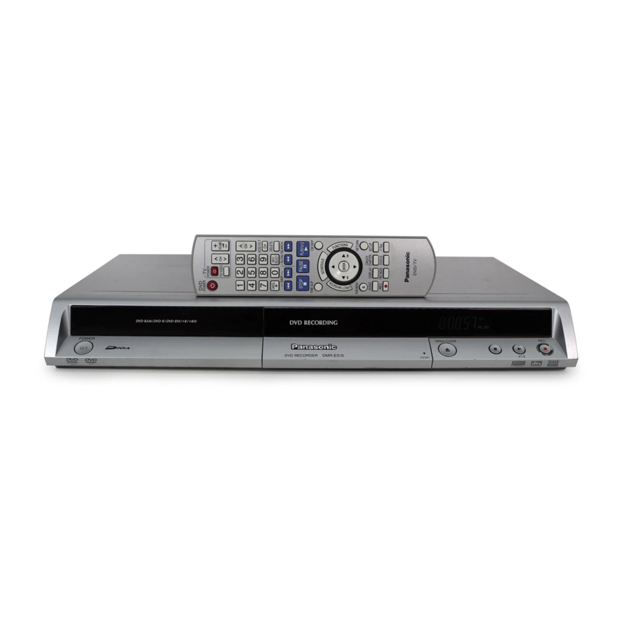
Summary of Contents for Panasonic DMR-ES15EE
- Page 1 ORDER NO.CHM0603012CE DVD Recorder DMR-ES15EE / DMR-ES15GC / DMR-ES15GCS / DMR- ES15GN / DMR-ES15GCA Vol. 1 Colour (S).......Silver Type SPECIFICATIONS...
-
Page 2: Safety Precaution
1. Safety Precaution 1.1. General guidelines 1. When servicing, observe the original lead dress. If a short circuit is found, replace all parts which have been overheated or damaged by the short circuit. 2. After servicing, see to it that all the protective devices such as... - Page 3 insulation barriers, insulation papers shields are properly installed. 3. After servicing, make the following leakage current checks to prevent the customer from being exposed to shock hazards. 1.1.1. Leakage current cold check 1. Unplug the AC cord and connect a jumper between the two prongs on the plug.
-
Page 4: Prevention Of Electrostatic Discharge (Esd) To Electrostatic Sensitive (Es) Devices
leakage current tester (Simpson Model 229 or equivalent) may be used to make the hot checks, leakage current must not exceed 1/2 milliampere. In case a measurement is outside of the limits specified, there is a possibility of a shock hazard, and the equipment should be repaired and rechecked before it is returned to the customer. - Page 5 comparable conductive material). 7. Immediately before removing the protective material from the leads of a replacement ES device, touch the protective material to the chassis or circuit assembly into which the device will be installed. Caution Be sure no power is applied to the chassis or circuit, and observe all other safety precautions.
-
Page 6: Service Caution Based On Legal Restrictions
2.3. Service caution based on legal restrictions 2.3.1. General description about Lead Free Solder (PbF) The lead free solder has been used in the mounting process of all electrical components on the printed circuit boards used for this equipment in considering the globally environmental conservation. -
Page 7: Service Navigation
Note * Ingredient: tin (Sn), 96.5%, silver (Ag) 3.0%, Copper (Cu) 0.5%, Cobalt (Co) / Germanium (Ge) 0.1 to 0.3% 3. Service Navigation 3.1. Service Information 3.2. Caution for DivX 4. Specifications... -
Page 9: New Feature
5. New Feature 5.1. About DivX 5.1.1. General DivX is a new video compressing format that is applied MPEG4 technology to improve image quality and the compressibility, and it is developed by the DivXNetworks, Inc., Video file of high resolution and the high picture quality can be made though it is a high compressibility. DivX codec is necessary for converting video to DivX file and .playback files made. - Page 10 5.1.2. Operating Instructions about DivX Video-on-Demand Content DivX Video-on-Demand (VOD) content is encrypted for copyright protection. In order to play DivX VOD content on this unit, you first need to register the unit. Follow the on line instructions for purchasing DivX VOD content to enter unit's registration code and register unit.
- Page 14 5.1.3. About DivX DRM Divx file includes file to which DRM(Digital Right Management) is applied and file not applied. This item is a content that relates only in treating file to which DRM is applied. 1. Registration Code display function 2.
- Page 15 Moreover, Registration code is updated by new user authentication ever if same recorder. 2) User's registration and approval function - Only one user can register for one recorder. If user's registration is not done with the recorder, DivX file cannot be played back. - User's registration is performed only when a DivX DRM file is first chosen by recorder - DivX DRM file that can perform user's registration is only a file that...
-
Page 16: Location Of Controls And Components
When it has reached head of title, the playback is ended, and screen becomes DivX menu (There is no resume) and then cursor is located on title that has been played back. Then if the same file was continuously played back, it begins to playback from the file head. - Page 17 7. Operation Instructions 7.1. Taking out the Disc from DVD-Drive Unit when the Disc cannot be ejected by OPEN/CLOSE button...
- Page 18 7.1.1. Forcible Disc Eject 7.1.1.1. When the power can be turned off. 1. Turn off the power and press [STOP] [CH UP] keys on the front panel simultaneously for 5 seconds. 7.1.1.2. When the power can not be turned off. 1.
-
Page 19: Service Mode
8. Service Mode 8.1. Self-Diagnosis and Special Mode Setting 8.1.1. Self-Diagnosis Functions Self-Diagnosis Function provides information for errors to service personnel by “Self-Diagnosis Display” when any error has occurred. U**, H** and F** are stored in memory and held. You can check latest error code by transmitting [0] [1] of Remote Controller in Service Mode. Automatic Display on FL will be cancelled when the power is turned off or AC input is turned off during self-diagnosis display is ON. - Page 20 Error Diagnosis contents Description Monitor Automatic FL Code Display The unit is carrying No display out its recovery process. Hang-up Displayed when communication No display error has occurred between Main microprocessor and Timer microprocessor. Displayed is left [POWER] key is No error information Initial setting for error code in No display...
- Page 21 Error Diagnosis contents Description Monitor Automatic FL Code Display Restoration operation Since the power cord fell out No display PLEASE during a power failure or WAIT operation, it is under restoration operation. *It will OK, if a display disappears automatically. If a display does not disappear, there is the possibility that defective ---------------------------------...
- Page 22 Item FL display Key operation Mode name Description Front Key TEST Mode *All the main unit's parameters Press [STOP], [CH (include tuner) are initialized. and [OPEN/CLOSE] simultaneously seconds when power off. Rating password The audiovisual level setting Open the tray, and password is initialized to “Level [REC] and [PLAY] 8”.
- Page 23 Item FL display Key operation Mode name Description Front Key Forced power-off When the power button is not Display in P-off mode. Press [Power] key effective while power is ON, turn than 10 seconds. off the power forcibly. *When Timer REC is ON or EXT- LINK is ON, execute “Forced Power-off”...
- Page 24 Item FL display Key operation Mode name Description Front Key Aging Contents (Example): Demonstration Ejection of the disc is prohibited. *When lock the tray. When the power lock/unlock press [STOP] and The lock setting is effective until [POWER] keys unlocking the tray and not simultaneously released by “Main unit seconds.
- Page 25 simultaneously for five seconds. Item FL display Key operation Mode name Description (Remote controller Release Items Item of Service Mode executing Press [0] [0] or [ is cancelled. service mode. Error Code Last Error Code of U/H/F held by Press [0] [1] in service Display Timer is displayed on FL.
- Page 26 Item FL display Key operation Mode name Description (Remote controller Magenta Picture Magenta picture is output with *Initial mode is “Interlace”. Press [1] [2] in service Output Component Output from AV mode. Decoder. *Magenta picture (Saturation rate: 100%) Switch Interlace/ Press [1] [4] in Magenta *It is enable to switch Interlace/ Progressive...
- Page 27 Item FL display Key operation Mode name Description (Remote controller Audio Pattern The audio pattern stored in the Initial mode (Audio 48kHz) Press [2] [3] in service Output internal memory is output mode. (Lch: 1kHz/-18dB) (Rch: 400Hz/-18dB) Audio 44.1kHz/48kHz Press [2] [4] in Audio *Audio sound clock switching switching Pattern Output mode.
- Page 28 Item FL display Key operation Mode name Description (Remote controller RAM Drive Last RAM Drive error code display. 1. Error Number is Press [4] [2] in service Error displayed for 5 seconds. mode. *For details about the drive error code, refer to the Service Manual When “INFO**** for the specific RAM Drive.
- Page 29 Item FL display Key operation Mode name Description (Remote controller Delete the Last Delete the Last Drive Error Press [9] [6] in service Drive Error information stored on the DVD mode. RAM-Drive. Laser power Drive state is judged based on confirmation difference between laser power into RAM Drive in service...
- Page 30 Item FL display Key operation Mode name Description (Remote controller Display the Display the accumulated unit's Press [6] [4] in service accumlated working time. mode. working time (Indicating unit: Second) Display the Error Display the Error History stored Display reason of error for Press [6] [5] in service History on the unit.
- Page 31 Item FL display Key operation Mode name Description (Remote controller Delete the Error Delete Error History information Press [9] [7] in service History stored on the unit. mode. AV4(V)/AV1(RGB) I Set input to AV4 (V) and set Press [8] [0] in service /O Setting output to AV1 (RGB) for I/O mode.
-
Page 32: Service Fixture And Tools
Item FL display Key operation Mode name Description (Remote controller Finishing service Release Service Mode. Display in STOP (E-E) Press power button mode mode. the front panel or controller in service 9. Service Fixture & Tools Part Number Description Compatibility RFKZ0365 Extension Cable (MainP.C.B. - Page 33 10.3. Top Case 1. Remove 2 screws (A) and 3 screws (B). 2. Slide Top Case rearward and open the both ends at rear side of the Top Case a little and lift the Top Case in the direction of the arrows.
-
Page 34: Ram/Digital P.c.b. Module
1. Unlock 6 tabs in (A) - (F) turn. Pull with the front panel in the direction of your side. 10.5. RAM/Digital P.C.B. Module Note: After replacing RAM/Digital P.C.B. Module, “TM AV1” is displayed on FL. Once power off, start-up again. 1. - Page 35 3. Put Digital P.C.B. on RAM Drive and remove RAM/Digital P.C.B. Module. Note: RAM/Digital P.C.B. Module as service part has no heat sink unit. Before returning to customer, heat sink unit should be installed on Digital P.C.B..
- Page 36 10.6. DV Jack P.C.B. 1. Remove 1 Screw (A) to remove DV jack P.C.B. 10.7. Power P.C.B. 1. Remove 1 Screw (A).
- Page 37 2. Remove 3 Screws (B) and disconnect Connector (A). 3. Unlock Power P.C.B. from a Flange to remove Power P.C.B. 10.8. Rear Panel 1. Remove 7 Screws (A) and 1 Screw (B). 2. Unlock 2 Locking Tabs (A) to remove Rear Panel.
- Page 38 10.9. Main P.C.B. and Front (L) P.C.B. 1. Remove 9 Screws (A) and 1 Screw (B). 2. Remove Digital Angle to remove Main P.C.B. and Front (L) P.C.B.. 10.10. Tuner P.C.B. 1. Pull out the Tuner P.C.B. in the direction of the arrow.
-
Page 39: Measurements And Adjustments
11. Measurements and Adjustments 11.1. Service Positions Note: For description of the disassembling procedure, see the section 10. 11.1.1. Checking and Repairing of Power P.C.B. 11.1.2. Checking and Repairing of RAM / Digital P.C.B. Module... - Page 40 11.1.3. Checking and Repairing of Main P.C.B.
-
Page 41: Caution For Replacing Parts
11.2. Caution for Replacing Parts 11.2.1. Items that should be done after replacing parts... -
Page 42: Standard Inspection Specifications After Making Repairs
11.2.2. Notice after replacing RAM/Digital P.C.B. Module After replacing RAM/Digital P.C.B. Module, “TM AV1” is displayed on FL. Once power off, and start-up again. 11.3. Standard Inspection Specifications after Making Repairs After making repairs, we recommend performing the following inspection, to check normal operation. -
Page 43: Block Diagram
Turn on the power, and confirm items pointed Items pointed out should reappear. out. Insert RAM disc. The Panasonic RAM disc should be recognized. Enter the EE (TU IN / AV IN - AV OUT) mode. No abnormality should be seen in the picture, sound or operation. -
Page 44: Schematic Diagram
13. Schematic Diagram 13.1. Interconnection Schematic Diagram 13.2. Power Supply Schematic Diagram 13.3. Main Net (1/4) Section (Main P.C.B. (1/4)) Schematic Diagram 13.4. Main Net (2/4) Section (Main P.C.B. (1/4)) Schematic Diagram 13.5. Main Net (3/4) Section (Main P.C.B. (1/4)) Schematic Diagram 13.6. -
Page 45: Tuner P.c.b. And Dv Jack P.c.b
14.2. Main P.C.B. 14.2.1. Main P.C.B. (1/4 Section) 14.2.2. Main P.C.B. (2/4 Section) 14.2.3. Main P.C.B. (3/4 Section) 14.2.4. Main P.C.B. (4/4 Section) 14.2.5. Main P.C.B. Address Information 14.3. Tuner P.C.B. and DV Jack P.C.B. 14.4. Front (L) P.C.B. 15. Appendix for Schematic Diagram 15.1. - Page 46 INITIAL/LOGO ABBREVIATIONS A0~UP ADDRESS ACLK AUDIO CLOCK AD0~UP ADDRESS BUS ADATA AUDIO PES PACKET DATA ADDRESS LATCH ENABLE AMUTE AUDIO MUTE AREQ AUDIO PES PACKET REQUEST AUDIO RF SERVO AMP INVERTED INPUT SERVO AMP OUTPUT ASYNC AUDIO WORD DISTINCTION SYNC BIT CLOCK (PCM) BCKIN BIT CLOCK INPUT...
- Page 47 INITIAL/LOGO ABBREVIATIONS DACCK D/A CONVERTER CLOCK DEEMP DEEMPHASIS BIT ON/OFF DEMPH DEEMPHASIS SWITCHING DIG0~UP FL DIGIT OUTPUT DATA INPUT DMSRCK DM SERIAL DATA READ CLOCK DMUTE DIGITAL MUTE CONTROL DROP OUT DOUT0~UP DATA OUTPUT DATA SLICE RF (BIAS) DROP OUT SIGNAL DRPOUT DATA REQUEST DREQ...
- Page 48 INITIAL/LOGO ABBREVIATIONS IECOUT IEC958 FORMAT DATA OUTPUT IPFRAG INTERPOLATION FLAG IREF I (CURRENT) REFERENCE ISEL INTERFACE MODE SELECT LDON LASER DIODE CONTROL LASER POWER CONTROL LRCK L CH/R CH DISTINCTION CLOCK MA0~UP MEMORY ADDRESS MEMORY CLOCK MCKI MEMORY CLOCK INPUT MCLK MEMORY SERIAL COMMAND CLOCK...
- Page 49 INITIAL/LOGO ABBREVIATIONS READ ENABLE RFENV RF ENVELOPE RF PHASE DIFFERENCE OUTPUT (CD-ROM) REGISTER SELECT RSEL RF POLARITY SELECT RESET RESERVE SBI0, 1 SERIAL DATA INPUT SBO0 SERIAL DATA OUTPUT SBT0, 1 SERIAL CLOCK SERIAL DATA CLOCK SCKR AUDIO SERIAL CLOCK RECEIVER SERIAL CLOCK SCLK...
- Page 50 SUB CODE Q DATA SYSCLK SYSTEM CLOCK INITIAL/LOGO ABBREVIATIONS TRACKING ERROR TIBAL BALANCE CONTROL BALANCE OUTPUT 1 BALANCE INPUT BALANCE INPUT BALANCE OUTPUT 2 TPSN OP AMP INPUT TPSO OP AMP OUTPUT TPSP OP AMP INVERTED INPUT TRCRS TRACK CROSS SIGNAL TRON TRACKING ON TRSON...
-
Page 51: Parts And Exploded Views
INITIAL/LOGO ABBREVIATIONS X' TAL XALE X ADDRESS LATCH ENABLE XAREQ X AUDIO DATA REQUEST XCDROM X CD ROM CHIP SELECT X CHIP SELECT XCSYNC X COMPOSITE SYNC X DATA STROBE XHSYNCO X HORIZONTAL SYNC OUTPUT XHINT XH INTERRUPT REQUEST X' TAL OSCILLATOR INPUT XINT X INTERRUPT X MEMORY WRITE ENABLE... - Page 52 16.1.2. Packing & Accessories Section...
-
Page 53: Replacement Parts List
16.2. Replacement Parts List Notes: *Important safety notice: Components identified by mark have special characteristics important for safety. Furthermore, special parts which have purposes of fire-retardant (resistors), high-quality sound (capacitors), low-noise (resistors), etc. are used. When replacing any of components, be sure to use only manufactures specified parts shown in the parts list. - Page 54 PAVCSG. Ref. No. Part No. Part Name & Description Remarks RFKB79119ET MAIN P.C.B. (RTL)EE RFKB79119FT MAIN P.C.B. (RTL)GCS,GC,GN,GCA C1502 ECJ2VB1E104K 25V 0.1U C1503 F2A1A6810022 10V 680P C1504 F2A1E1010067 25V 100U C1506 EEUFM1E221B 25V 220U C1508 F1H1A105A028 10V 1U C1509 ECJ1VB1H103K 50V 0.01U C1510 F1H1A105A028...
- Page 55 Ref. No. Part No. Part Name & Description Remarks C3026 ECJ1VB0J105K 6.3V 1U C3027 ECJ1VB1C104K 16V 0.1U C3028 ECJ1VB0J105K 6.3V 1U C3029 ECJ1VB1C104K 16V 0.1U C3031 ECJ1VB1H103K 50V 0.01U C3032 ECEA0JKA101B 6.3V 100U C3033 ECJ1VB1H103K 50V 0.01U C3034 ECJ1VB1H103K 50V 0.01U C3035 ECEA0JKA101B 6.3V 100U...
- Page 56 Ref. No. Part No. Part Name & Description Remarks C4057 F1J1H330A688 50V 33U C4059 ECQV1H104JL3 50V 0.1U C4060 F1J1H330A688 50V 33U C4061 ECJ1VF1C104Z 16V 0.1U C4062 F2A1C470A637 16V 47U C4063 F2A1C470A637 16V 47U C4064 F2A1C470A637 16V 47U C4065 ECJ1VF1C104Z 16V 0.1U C4067 F2A1E4700048 25V 47U...
- Page 57 Ref. No. Part No. Part Name & Description Remarks C7503 F1J0J475A008 6.3V 4.7U C7504 ECJ1VB1C104K 16V 0.1U C7505 ECJ1VB1C104K 16V 0.1U C7507 ECJ1VB1C104K 16V 0.1U C7509 ECJ1VB1C104K 16V 0.1U C7510 ECJ1VB1C104K 16V 0.1U C7511 ECJ1VC1H101J 50V 100P C7512 ECJ1VB1C104K 16V 0.1U C7513 F2A1V390A386 35V 39U...
- Page 58 Ref. No. Part No. Part Name & Description Remarks D7501 B0BA03600021 DIODE D7502 B0ACCK000005 DIODE D7504 MAZ4220NLF DIODE D7505 B0AADM000003 DIODE D7506 B0AADM000003 DIODE D7507 B0JAMD000026 DIODE D7508 MAZ4180NHF DIODE D7509 B0JDCE000002 DIODE D7510 MA2C165001VT DIODE DP7501 A2BD00000144 DISPLAY TUBE IC1501 C0DAZJH00003 IC1505...
- Page 59 Ref. No. Part No. Part Name & Description Remarks K7508 ERJ3GEY0R00V 1/10W 0 L4901 G0C220KA0065 COIL 22UH L7303 G0C1R0JA0019 COIL 1UH L7304 G0C2R2JA0019 COIL 2.2UH L7401 G0A220GA0026 COIL 22UH L7402 G0A220GA0026 COIL 22UH L7501 G0C390JA0055 COIL 39UH LB1502 J0JKB0000003 COIL LB1503 J0JKB0000003 COIL...
- Page 60 Ref. No. Part No. Part Name & Description Remarks LB7501 ERJ3GEY0R00V 1/10W 0 LB7502 ERJ3GEY0R00V 1/10W 0 LB7507 ERJ3GEY0R00V 1/10W 0 LB7508 ERJ3GEY0R00V 1/10W 0 LB7509 J0JCC0000060 COIL LB7510 ERJ3GEY0R00V 1/10W 0 LB7515 ERJ3GEY0R00V 1/10W 0 LB7516 ERJ3GEY0R00V 1/10W 0 LB7517 ERJ3GEY0R00V 1/10W 0...
- Page 61 Ref. No. Part No. Part Name & Description Remarks R3009 ERJ3GEYJ104V 1/10W 100K R3054 ERJ3GEYJ750V 1/10W 75 R3055 ERJ3GEYJ750V 1/10W 75 R3056 ERJ3GEYJ750V 1/10W 75 R3057 ERJ3GEYJ750V 1/10W 75 R3058 ERJ3GEYJ750V 1/10W 75 R3059 ERJ3GEYJ750V 1/10W 75 R3060 ERJ3GEYJ750V 1/10W 75 R3061 ERJ3GEYJ750V 1/10W 75...
- Page 62 Ref. No. Part No. Part Name & Description Remarks R4047 D0HB682ZA002 1/16W 6.8K R4055 D0HB123ZA002 1/16W 12K R4057 D0HB123ZA002 1/16W 12K R4066 D0HB103ZA002 1/10W 10K R4067 D0HB103ZA002 1/10W 10K R4071 ERJ3GEYJ473V 1/10W 47K R4074 ERJ3GEYJ473V 1/10W 47K R4076 ERJ3GEYJ821V 1/10W 820 R4077 ERJ3GEYJ101V 1/10W 100...
- Page 63 Ref. No. Part No. Part Name & Description Remarks R7510 ERJ3GEYJ101V 1/10W 100 R7517 ERJ3GEYJ472V 1/10W 4.7K R7518 ERJ3RBD273V 1/16W 27K R7520 ERJ3GEYJ103V 1/10W 10K R7521 ERJ3GEY0R00V 1/10W 0 R7523 ERJ3GEY0R00V 1/10W 0 R7527 ERJ3GEYJ101V 1/10W 100 R7528 ERJ3GEYJ101V 1/10W 100 R7529 ERJ3GEYJ101V 1/10W 100...
- Page 64 Ref. No. Part No. Part Name & Description Remarks R7614 ERJ3GEYJ470V 1/10W 47 R7615 ERJ3GEYJ473V 1/10W 47K R7616 ERJ3GEYJ473V 1/10W 47K R7617 ERDS2TJ271T 1/4W 270 R7619 ERJ3GEYJ103V 1/10W 10K R7620 ERJ3GEYJ473V 1/10W 47K R7621 ERJ3GEYJ104V 1/10W 100K R7622 ERJ3GEYJ153V 1/10W 15K R7623 ERJ3GEYJ181V 1/10W 180...
- Page 65 Ref. No. Part No. Part Name & Description Remarks W527 ERJ3GEY0R00V 1/10W 0 W528 ERJ3GEY0R00V 1/10W 0 W529 ERJ6GEY0R00V 1/8W 0 W530 ERJ6GEY0R00V 1/8W 0 W531 ERJ6GEY0R00V 1/8W 0 W532 ERJ6GEY0R00V 1/8W 0 W533 ERJ6GEY0R00V 1/8W 0 W534 ERJ3GEY0R00V 1/10W 0 W535 ERJ3GEY0R00V 1/10W 0...
- Page 66 Ref. No. Part No. Part Name & Description Remarks TU7801 ENGF7502GF TUNER W501 ERJ6GEY0R00V 1/8W 0 W502 ERJ3GEY0R00V 1/10W 0 W503 ERJ6GEY0R00V 1/8W 0 W504 ERJ6GEY0R00V 1/8W 0 W505 ERJ6GEY0R00V 1/8W 0 W506 ERJ3GEY0R00V 1/10W 0 W507 ERJ3GEY0R00V 1/10W 0 W508 ERJ6GEY0R00V 1/8W 0...
- Page 67 Ref. No. Part No. Part Name & Description Remarks S7002 EVQ11A04M SWITCH,POWER VEP71109A POWER SUPPLY P.C.B. (RTL) C1120 ECQU2A683MLC 100V 0.068U C1121 ECQU2A223MLC 100V 0.022U C1122 F1B2G1020002 400V 1000P C1123 F1B2G1020002 400V 1000P C1125 F1B2G1020002 400V 1000P C1143 F2B2W4700003 450V 47U C1150 EEUFM1V680B 35V 68U...
- Page 68 Ref. No. Part No. Part Name & Description Remarks P1101 K2AA2H000007 AC INLET P1102 K1KB19AA0032 CONNECTOR(19P) Q1200 B3PBA0000402 PHOTO COUPLER R1150 ERJ6GEYJ180V 1/8W 18 R1151 ERJ6GEYJ682V 1/8W 6.8K R1152 ERJ6GEYJ103V 1/8W 10K R1153 ERJ6GEYJ180V 1/8W 18 R1154 ERJ6GEYG682V 1/8W 6.8K R1155 ERJ6GEYG512V 1/8W 5.1K...
- Page 69 Ref. No. Part No. Part Name & Description Remarks RHD30111-3J SCREW RHD30119-L SCREW RMA1979A DIGITAL ANGLE A RFKNES15EE RAN/DIGITAL P.C.B. MODULE RFKNES15GCS RAN/DIGITAL P.C.B. MODULE RFKNES15GC RAN/DIGITAL P.C.B. MODULE RFKNES15GN RAN/DIGITAL P.C.B. MODULE RFKNES15GCA RAM/DIGITAL P.C.B. MODULE RMQ1513 HEAT TRANSFER SHEET RKA0144-K FOOT RUBBER RMC0672...
-
Page 70: Schematic Diagram For Printing With A4
(IC)GCS Ref. No. Part No. Part Name & Description Remarks RQT8326-A OPERATING INSTRUCTIONS (ID)GC,GCA RPG7932 PACKING CASE RPG7935 PACKING CASE RPG7934 PACKING CASE RPG7933 PACKING CASE RPG8054 PACKING CASE RPN1863A CUSHION RPFC0026-B POLYETHYLENE BAG RPN1863B CUSHION 17. Schematic Diagram for printing with A4... -
Page 71: Timer (3/4) Section (Main P.c.b. (4/4)) Schematic Diagram (T)
13.14. Timer (3/4) Section (Main P.C.B. (4/4)) Schematic Diagram (T) TIMER SECTION (1/4) TL7515 R7516 22(EC) R7527 G_CSYNC_A G_CSYNC_IN_A C7518 C7519 C7516 X7501 C7517 R7531 100K H0D100500018 X7502 R7532 3300 H0D100500019 H0A327200108 R7533 C7524 R7534 R7535 R7536 R7537 LB7508 IC7502 ERJ3GEY0R00V C0EBE0000504 R7543... - Page 72 [52]NC(OPEN) SYS2 R7653 [51]FL_RESET NC(OPEN) TEST2[H] CL7502 LB7508 NC(OPEN) HDMI_HOTPLUG ERJ3GEY0R00V NC(OPEN) CL7503 NC(OPEN) R7543 C7551 IIC_CLK R7544 IIC_DATA 42 43 R7520 TL7510 C7532 C7531 Net Section:(Page: O Section:(Page: m Decoder Section:(Page: DMR-ES15EE/GC/GCS/GN/GCA Section:(Page: TIMER(3/4) Section (Main P.C.B.(4/4)) Schematic Diagram(T)
-
Page 73: Timer (4/4) Section (Main P.c.b. (4/4)) Schematic Diagram (T)
13.15. Timer (4/4) Section (Main P.C.B. (4/4)) Schematic Diagram (T) M N O P Q TIMER SECTION (2/4) QR75 UNR52 R7586 D7502 R7583 R7584 B0ACCK000005 4700 (1SS355) R7585 R7587 2R2M 220K C7552 R7588 R7589 220P 100K LB7510 ERJ3GEY0R00V EXT_LINK CH_DOW S7501(EE) S7502 EVQ11A04M... - Page 74 R7642 5600 Main Net Section:(Page: A/V I/O Section:(Page: :Nicam Decoder Section:(Page: DMR-ES15EE/GC/GCS/GN/GCA imer Section:(Page: NOTE:DO NOT USE THE PART NUMBER SHOWN ON THIS DRAWING FOR ORDERRING. TIMER(4/4) Section THE CORRECT PART NUMBER IS SHOWN IN THE PARTS LIST,AND MAY BE SLIGHTLYDIFFERNT OR AMENDED SINCE THIS DRAWING WAS PREPARED.
-
Page 75: Tuner Pack Schematic Diagram
13.16. Tuner Pack Schematic Diagram TO PP7401 MAIN P.C.B. (MAIN NET(2/4) SECTION) C7809 0.01 PS7801 K1KB18B00012 BOOSTER_5V RFC_AUDIO RFC_A_MUTE PS_5V CPS_V_OUT JC_REG_5V IIC_CLK IIC_DATA AUDIO_OUT K7810 ERJ3GEY0R00V SIF_OUT UNREG_38V TUNER_VIDEO1 (TO MAIN) Q7802 2SB1218A0L (EP/EBL) R784... - Page 76 R7820 1000 R7844 NOTE:DO NOT USE THE PART NUMBER SHOWN ON THIS DRAWING FOR ORDERRING. DMR-ES15EE/GC/GCS/GN/GCA THE CORRECT PART NUMBER IS SHOWN IN THE PARTS LIST,AND MAY BE SLIGHTLYDIFFERNT OR AMENDED SINCE THIS DRAWING WAS PREPARED. Tuner Pack Schematic Diagram...
-
Page 77: Front (L) Schematic Diagram
JW7001 [VWJ02F0060VV] KEY3_POWER NOTE:DO NOT USE THE PART NUMBER SHOWN ON THIS DRAWING FOR ORDERRING. DMR-ES15EE/GC/GCS/GN/GCA THE CORRECT PART NUMBER IS SHOWN IN THE PARTS LIST,AND MAY BE SLIGHTLYDIFFERNT OR AMENDED SINCE THIS DRAWING WAS PREPARED. Front(L) Schematic Diagram 13.18. DV Jack Schematic Diagram TO PS57001 DIGITAL P.C.B. - Page 81 IC1501 IC1505 IC1506 Ref No. MODE 12.3 12.3 12.4 PLAY 12.3 12.3 12.4 STOP 12.3 12.3 12.4 IC1507 IC1510 IC1520 Ref No. MODE PLAY STOP IC1521 Ref No. MODE PLAY STOP IC3001 Ref No. MODE PLAY STOP IC3001 Ref No. MODE PLAY STOP...
- Page 82 IC7302 IC7401 IC7402 Ref No. MODE 12.4 11.6 PLAY 12.4 11.6 STOP 12.4 11.6 IC7403 IC7404 Ref No. MODE PLAY STOP IC7501 Ref No. MODE PLAY STOP IC7501 Ref No. MODE PLAY STOP IC7501 Ref No. MODE -0.1 PLAY -0.1 STOP -0.1 IC7501...
- Page 83 P59001 Ref No. MODE 12.3 12.3 PLAY 12.3 12.3 STOP 12.3 12.3 Ref No. P59001 MODE PLAY STOP P59001 Ref No. MODE 12.3 12.3 12.3 12.3 12.3 PLAY 12.3 12.3 12.3 12.3 12.3 STOP 12.3 12.3 12.3 12.3 12.3 P59001 Ref No.
- Page 84 IC1150 IC1200 Ref No. MODE 11.6 -1523 PLAY 11.6 -1523 STOP 11.6 -1538 Q1200 Ref No. MODE PLAY STOP...
- Page 85 Q7802 Ref No. MODE PLAY STOP...
- Page 86 T1150-4,5 STOP T1150-6 STOP T1150-2,3 STOP T1150-8 STOP 15Vp-p (5 sec.div) 30Vp-p (5 sec.div) 10Vp-p (5 sec.div) 30Vp-p (5 sec.div) IC1150-9 STOP T1150-12 STOP P7402-17,19 REC/PLAY IC1150-1 STOP 580Vp-p (5 sec.div) 10Vp-p (2m sec.div) 0.8Vp-p (1m sec.div) 10.0Vp-p (5 sec.div) P7402-51 REC/PLAY P7402-39 REC/PLAY P7402-47 REC/PLAY...
- Page 87 IIC CLK SIF OUT FROM IC7501- IIC BUS TIMER LOGIC TUN Lch IIC DATA SECTION L OUT IC7501- RF OUT MUTE TUNER P.C.B. IC4901 OPTICAL (DIGITAL AUDIO OUT) FROM P59001 P7402 IEC OUT DIGITAL P.C.B. DMR-ES15EE/GC/GCS/GN/GCA Analog Audio Block Diagram...
- Page 88 DI POWER ON IC1506- TU P ON TU POWER ON IC1510- G SCLK A SCLK TBUS CLK P7402- TO/FROM G SBPTM A SBPTM TBUS TXD DIGITAL P.C.B. P7402- G SBMTP A SBMTP TBUS RXD P7402- DMR-ES15EE/GC/GCS/GN/GCA Analog Timer Block Diagram...
- Page 89 TU7801 GREEN (EP/EBL) U/V TUNER (DECODER/EXT) AV2 B Q7802 TUNER BLUE AV2 G PP7401 PS7801 VIDEO CLAMP CLAMP BUFFER AV2 V/Y VIDEO/Y 2.3V (Except (EP/EBL)) AV2 B CLAMP 1.0V K7809 AV2 V/Y TUNER P.C.B. CLAMP DMR-ES15EE/GC/GCS/GN/GCA Analog Video Block Diagram...
- Page 90 ,IC4012- 12,13,14,15 Q1200 (FEED BACK) FROM PWR SAVE TIMER IC7501- 79 SECTION QR7401 :ON) IC1501 (REG.DR+12V) VOUT DR+12V FROM DR P ON IC1200 TIMER IC7501- 42 SECTION (ERROR VOLTAGE DET.) COLD QR1501 :ON) QR1502 :ON) DMR-ES15EE/GC/GCS/GN/GCA Power Supply Block Diagram...
- Page 91 IC59501 Q59501 (DC-DC CONVERTER) (REG.D+1.2V) IC1510 (REG.+5V) D+1.2V P7402 P59001 (+1.2V) 52,54,56,58,60,62 VOUT JC REG.+5V ON/OFF 2 FROM TU P ON TIMER IC7501- 43 SECTION IP50001 DR+12V P7402 P59001 IC50003(+12V) DMR-ES15EE/GC/GCS/GN/GCA DMR-ES15EE/GC/GCS/GN/GCA Power Supply Block Diagram Power Supply Block Diagram...
- Page 92 Front (L) P.C.B. DMR-ES15EE/GC/GCS/GN/GCA FRONT (L) P.C.B. (VEP70161A)
- Page 93 Main P.C.B. Integrated Circuit TL7505 LB3913 C3011 C4061 C7524 R3927 R7412 R7608 IC1501 TL7509 LB7301 C3012 C4062 C7528 R3928 R7414 R7612 IC1505 TL7510 LB7302 C3013 C4063 C7531 R3929 R7444 R7614 IC1506 TL7511 LB7303 C3014 C4064 C7532 R3930 R7445 R7615 IC1507 TL7512 LB7304 C3015...
- Page 94 (EE) Location Map (REAR) (FRONT) DMR-ES15EE/GC/GCS/GN/GCA Main P.C.B. (RFKB79119ET:ES15EE, RFKB79119FT:ES15GC/GCS/GN/GCA) (1/4 Section)
- Page 95 Location Map (REAR) (FRONT) DMR-ES15EE/GC/GCS/GN/GCA Main P.C.B. (RFKB79119ET:ES15EE, RFKB79119FT:ES15GC/GCS/GN/GCA) (2/4 Section)
- Page 96 Main P.C.B. (EC) Location Map (REAR) (FRONT) DMR-ES15EE/GC/GCS/GN/GCA Main P.C.B. (RFKB79119ET:ES15EE, RFKB79119FT:ES15GC/GCS/GN/GCA) (3/4 Section)
- Page 97 Location Map (REAR) (FRONT) DMR-ES15EE/GC/GCS/GN/GCA Main P.C.B. (RFKB79119ET:ES15EE, RFKB79119FT:ES15GC/GCS/GN/GCA) (4/4 Section)
- Page 98 Power P.C.B. Integrated Circuit Fuse Transister Transformer Capacitor Connector Coil Resistor Diode Power P.C.B. Absorber COLD DMR-ES15EE/GC/GCS/GN/GCA Power P.C.B. (VEP71109A)
- Page 99 DV Jack P.C.B. Tuner P.C.B. DMR-ES15EE/GC/GCS/GN/GCA DMR-ES15EE/GC/GCS/GN/GCA Tuner P.C.B. DV JACK P.C.B. (VEP07A91D) (VEP73135A)
- Page 100 QR4003 XDMUTE UNR521100L (UN5211-TX) NOTE:DO NOT USE THE PART NUMBER SHOWN ON THIS DRAWING FOR ORDERRING. DMR-ES15EE/GC/GCS/GN/GCA A/V I/O SECTION THE CORRECT PART NUMBER IS SHOWN IN THE PARTS LIST,AND MAY BE (3/4) A/V I/O(1/4) Section SLIGHTLYDIFFERNT OR AMENDED SINCE THIS DRAWING WAS PREPARED.
- Page 101 LB3007 J0JBC0000011 C3059 1000P R4007 82K C3060 LB3008 470P J0JBC0000019 DMR-ES15EE/GC/GCS/GN/GCA F G H L M AS N O P Q R S Z AA AB AC AD AE AG AH AI AJ AK AL AM A/V I/O SECTION A/V I/O(2/4) Section (4/4) (Main P.C.B.(2/4))
- Page 102 DE:Nicam Decoder Section:(Page: NOTE:DO NOT USE THE PART NUMBER SHOWN ON THIS DRAWING FOR ORDERRING. THE CORRECT PART NUMBER IS SHOWN IN THE PARTS LIST,AND MAY BE DMR-ES15EE/GC/GCS/GN/GCA T:Timer Section:(Page: SLIGHTLYDIFFERNT OR AMENDED SINCE THIS DRAWING WAS PREPARED. A/V I/O(3/4) Section (Main P.C.B.(2/4))
- Page 103 G_IEC_OUT_A M:Main Net Section:(Page: AV:A/V I/O Section:(Page: DE:Nicam Decoder Section:(Page: DMR-ES15EE/GC/GCS/GN/GCA T:Timer Section:(Page: NOTE:DO NOT USE THE PART NUMBER SHOWN ON THIS DRAWING FOR ORDERRING. A/V I/O(4/4) Section THE CORRECT PART NUMBER IS SHOWN IN THE PARTS LIST,AND MAY BE SLIGHTLYDIFFERNT OR AMENDED SINCE THIS DRAWING WAS PREPARED.
- Page 104 100P R7317 AV:A/V I/O Section:(Page: DE:Nicam Decoder Section:(Page: T:Timer Section:(Page: DMR-ES15EE/GC/GCS/GN/GCA Nicam Decoder Section NOTE:DO NOT USE THE PART NUMBER SHOWN ON THIS DRAWING FOR ORDERRING. (Main P.C.B.(3/4)) THE CORRECT PART NUMBER IS SHOWN IN THE PARTS LIST,AND MAY BE SLIGHTLYDIFFERNT OR AMENDED SINCE THIS DRAWING WAS PREPARED.
- Page 105 TPB- TPB+ TPB- NOTE:DO NOT USE THE PART NUMBER SHOWN ON THIS DRAWING FOR ORDERRING. DMR-ES15EE/GC/GCS/GN/GCA THE CORRECT PART NUMBER IS SHOWN IN THE PARTS LIST,AND MAY BE SLIGHTLYDIFFERNT OR AMENDED SINCE THIS DRAWING WAS PREPARED. DV Jack Schematic Diagram...
- Page 106 (TIMER(4/4) SECTION) JW7001 [VWJ02F0060VV] KEY3_POWER NOTE:DO NOT USE THE PART NUMBER SHOWN ON THIS DRAWING FOR ORDERRING. DMR-ES15EE/GC/GCS/GN/GCA THE CORRECT PART NUMBER IS SHOWN IN THE PARTS LIST,AND MAY BE SLIGHTLYDIFFERNT OR AMENDED SINCE THIS DRAWING WAS PREPARED. Front(L) Schematic Diagram...
- Page 107 Detail Block Diagram IC1506 Detail Block Diagram PROTECTION VREF IC1507 Detail Block Diagram IC1510 Detail Block Diagram IC1520 Detail Block Diagram IC1521 Detail Block Diagram IC7401 Detail Block Diagram IC7402 Detail Block Diagram IC7403 Detail Block Diagram DMR-ES15EE/GC/GCS/GN/GCA IC-Detail Block Diagram...
- Page 108 AV1 Lch MUTE IIC BUS (SW10) LOGIC BIAS AV2 R/C CLAMP TUN Rch TUNER AV2 G TUN Lch CLAMP CLAMP AV2 B CLAMP RF OUT MUTE AV2 V/Y CLAMP IC3001 Detail Block Diagram IC4011 Detail Block Diagram DMR-ES15EE/GC/GCS/GN/GCA IC-Detail Block Diagram...
- Page 109 Ref.No.50000 SERIES CLOSE SW Main Net Ref.No.1500,7400 SERIES Ref.No.50000,53000,54000,55000,57000 SERIES Digital Main A/V I/O Ref.No.3000,3900,4000,4900 SERIES Audio I/O Ref.No.54000 SERIES P.C.B. P.C.B. Nicam Decoder Ref.No.3700 SERIES D Net Ref.No.59000 SERIES Timer Ref.No.7500,7600 SERIES Model Select Ref.No.59000 SERIES DMR-ES15EE/GC/GCS/GN/GCA Interconnection Schematic Diagram...
- Page 110 POWER P.C.B. P1501 K1KA19A00007 X_SW15R5V LB1504 X_SW5R8VT J0JKB0000003 X_SW5R8V X_SW5R8V X_SW5R8V X_SW5R8V LB1502 J0JKB0000003 G1501$ X_SW12V X_SW12V C1518 C1515 10V100 X_SW12V LB1506 F2A1E4700048 X_SW12V J0JKB0000003 X_SW3R8V X_SW3R8V P_ON_H X_SW3R8V DMR-ES15EE/GC/GCS/GN/GCA MAIN NET SECTION (3/4) Main Net(1/4) Section (Main P.C.B.(1/4)) Schematic Diagram(M)
- Page 111 THE CORRECT PART NUMBER IS SHOWN IN THE PARTS LIST,AND MAY BE K7403 VWJ0795=10 SLIGHTLYDIFFERNT OR AMENDED SINCE THIS DRAWING WAS PREPARED. C7439 Q7402 2SD1819A0L R7446 2000[D] UNREG_38V DMR-ES15EE/GC/GCS/GN/GCA Main Net(2/4) Section MAIN NET SECTION (4/4) (Main P.C.B.(1/4)) Schematic Diagram(M)
- Page 112 AV:A/V I/O Section:(Page: NOTE:DO NOT USE THE PART NUMBER SHOWN ON THIS DRAWING FOR ORDERRING. THE CORRECT PART NUMBER IS SHOWN IN THE PARTS LIST,AND MAY BE DMR-ES15EE/GC/GCS/GN/GCA DE:Nicam Decoder Section:(Page: SLIGHTLYDIFFERNT OR AMENDED SINCE THIS DRAWING WAS PREPARED. Main Net(3/4) Section T:Timer Section:(Page: (Main P.C.B.(1/4))
- Page 113 K9ZZ00001279 LOCATION MAP M:Main Net Section:(Page: AV:A/V I/O Section:(Page: DMR-ES15EE/GC/GCS/GN/GCA DE:Nicam Decoder Section:(Page: NOTE:DO NOT USE THE PART NUMBER SHOWN ON THIS DRAWING FOR ORDERRING. Main Net(4/4) Section THE CORRECT PART NUMBER IS SHOWN IN THE PARTS LIST,AND MAY BE T:Timer Section:(Page: SLIGHTLYDIFFERNT OR AMENDED SINCE THIS DRAWING WAS PREPARED.
- Page 114 THE CORRECT PART NUMBER IS SHOWN IN THE PARTS LIST,AND MAY BE COMPONENTS IDENTIFIED WITH THE MARK HAVE THE SPECIAL CHARACTERISTICS FOR SAFETY. SLIGHTLY DIFFERNT OR AMENDED SINCE THIS DRAWING WAS PREPARED. WHEN REPLACING ANY OF THESE COMPONENTS.ONLY THE SAME TYPE. DMR-ES15EE/GC/GCS/GN/GCA Power Supply Schematic Diagram...
- Page 115 ERJ3GEY0R00V C7520 C7534 0.01 NOTE:DO NOT USE THE PART NUMBER SHOWN ON THIS DRAWING FOR ORDERRING. DMR-ES15EE/GC/GCS/GN/GCA TIMER SECTION THE CORRECT PART NUMBER IS SHOWN IN THE PARTS LIST,AND MAY BE (3/4) TIMER(1/4) Section SLIGHTLYDIFFERNT OR AMENDED SINCE THIS DRAWING WAS PREPARED.
- Page 116 C0EBE0000457 RESET R7620 IC-DETAIL BLOCK DIAGRAM C7581 K7509 0.01 VWJ0795 QR7506 D3R3V UNR521200L C7583 R7622 0.47 D7509 B0JDCE000002 X_SW_5R2V Vref R7623 R7621 100K C7584 F4D55473A013 DMR-ES15EE/GC/GCS/GN/GCA M N O P Q TIMER SECTION TIMER(2/4) Section (4/4) (Main P.C.B.(4/4)) Schematic Diagram(T)
- Page 117 DE:Nicam Decoder Section:(Page: NOTE:DO NOT USE THE PART NUMBER SHOWN ON THIS DRAWING FOR ORDERRING. THE CORRECT PART NUMBER IS SHOWN IN THE PARTS LIST,AND MAY BE DMR-ES15EE/GC/GCS/GN/GCA T:Timer Section:(Page: SLIGHTLYDIFFERNT OR AMENDED SINCE THIS DRAWING WAS PREPARED. TIMER(3/4) Section (Main P.C.B.(4/4))
- Page 118 R7642 5600 M:Main Net Section:(Page: AV:A/V I/O Section:(Page: DE:Nicam Decoder Section:(Page: DMR-ES15EE/GC/GCS/GN/GCA T:Timer Section:(Page: NOTE:DO NOT USE THE PART NUMBER SHOWN ON THIS DRAWING FOR ORDERRING. TIMER(4/4) Section THE CORRECT PART NUMBER IS SHOWN IN THE PARTS LIST,AND MAY BE SLIGHTLYDIFFERNT OR AMENDED SINCE THIS DRAWING WAS PREPARED.
- Page 119 R7820 1000 R7844 NOTE:DO NOT USE THE PART NUMBER SHOWN ON THIS DRAWING FOR ORDERRING. DMR-ES15EE/GC/GCS/GN/GCA THE CORRECT PART NUMBER IS SHOWN IN THE PARTS LIST,AND MAY BE SLIGHTLYDIFFERNT OR AMENDED SINCE THIS DRAWING WAS PREPARED. Tuner Pack Schematic Diagram...
-
Page 120: Interconnection Schematic Diagram
13 Schematic Diagram 13.1. Interconnection Schematic Diagram POWER P7001 P7505 P7401 P59001 XINTP DR12V KEY3 POWER KEY3 POWER SCLK DR12V XINTM DRGND SBPTM FRONT(L) P.C.B. DRGND SBMTP DR5V XMPREQ DR5V AU5V ITM2A XDMUTE ITA2M PP7401 PS7801 AADC L P OFF L2 BOOSTER5V BOOSTER 5V AADC R... - Page 121 DIGITAL P.C.B. COILU COILV COILW FP50004 OPEN SW PHOTO LED CARTRIGE REC INH P.C.B.Name Circuit Name Ref.No. Ref.No.50000 SERIES CLOSE SW Ref.No.50000,53000,54000,55000,57000 SERIES Digital Audio I/O Ref.No.54000 SERIES P.C.B. D Net Ref.No.59000 SERIES Model Select Ref.No.59000 SERIES DMR-ES15EE/GC/GCS/GN/GCA Interconnection Schematic Diagram...
-
Page 122: Power Supply Schematic Diagram
13.2. Power Supply Schematic Diagram C1125 LB1122 LB1127 F1B2G1020002 VWJ0795=5 J0JHC0000048 ECKWNA102M ZA1103 ZA1104 D1140 EYF52BCY EYF52BCY B0EDKT000009 K3GE1ZA00010 K3GE1ZA00010 (S1WBA80-7062) L1120 L1121 G0B233D00001 G0B233D00001 C1121 F1101 ECQU2A223MLC T1150 K5D202BK0005 ETS28BF1Z6AD 250V T2AL P1101 K2AA2H000007 SEE THE SERVICE MANUAL LB1123 VWJ0795=5 LB1126 R1153... - Page 123 /VCC(STOP) PROTECTOR /VCC(STARTUP ON) IDP(LIMIIT/ BURST)SENS. ZERO CURRENT DET./ONDEAD TIMER CONTROL SOFT-DRIVE CIRCUIT CIRCUIT STANDBY CIRCUIT OCP THRESHOLD COMPARATOR/ RESTERT BURST MODE TIMER OCP THRESHOLD COMPARATOR ON WIDTH TIMER SOURCE /OCL HARACTERISTICS FOR SAFETY. YPE. DMR-ES15EE/GC/GCS/GN/GCA Power Supply Schematic Diagram...
-
Page 124: Main Net (1/4) Section (Main P.c.b. (1/4)) Schematic Diagram (M)
13.3. Main Net (1/4) Section (Main P.C.B. (1/4)) Schematic Diagram (M) LOCATION MAP X_SW_3R3V RESET_5R2V M:Main Net Section:(Page: AV:A/V I/O Section:(Page: DE:Nicam Decoder Section:(Page: T:Timer Section:(Page: NOTE:DO NOT USE THE PART NUMBER SHOWN ON THIS DRAWING FOR ORDERRING. THE CORRECT PART NUMBER IS SHOWN IN THE PARTS LIST,AND MAY BE SLIGHTLYDIFFERNT OR AMENDED SINCE THIS DRAWING WAS PREPARED. - Page 125 TUREG5V X_SW5R2V IC1510 C0CBCDG00006 (PG050DNA1ZPH) X_SW3R3 ANA5V ANA3R3V DMR-ES15EE/GC/GCS/GN/GCA TION Main Net(1/4) Section (Main P.C.B.(1/4)) Schematic Diagram(M)
-
Page 126: Main Net (2/4) Section (Main P.c.b. (1/4)) Schematic Diagram (M)
13.4. Main Net (2/4) Section (Main P.C.B. (1/4)) Schematic Diagram (M) ZJ7402 K9ZZ00001279 QR7401 UNR521300L (UN5213-TX) IC7401 PS11R6V C0CBCYG000 (PQ200WNA1Z K7403 VWJ0795=10 C7439 R7446 2000[D] MAIN NET SECTION (4/4) - Page 127 NOTE:DO NOT USE THE PART NUMBER SHOWN ON THIS DRAWING FOR ORDERRING. THE CORRECT PART NUMBER IS SHOWN IN THE PARTS LIST,AND MAY BE 7403 SLIGHTLYDIFFERNT OR AMENDED SINCE THIS DRAWING WAS PREPARED. J0795=10 Q7402 2SD1819A0L R7446 2000[D] UNREG_38V DMR-ES15EE/GC/GCS/GN/GCA Main Net(2/4) Section (Main P.C.B.(1/4)) Schematic Diagram(M)
-
Page 128: Main Net (3/4) Section (Main P.c.b. (1/4)) Schematic Diagram (M)
13.5. Main Net (3/4) Section (Main P.C.B. (1/4)) Schematic Diagram (M) MAIN NET SECTION (1/4) ANA5V P_OFF_L DR_P_ON_H ZJ7401 K9ZZ00001279 DR12V (M6520) IC1501 L1501 C0DAZJH00003 VWJ0795 ON[H] SENSE C1502 LOCATION MAP NOTE:DO NOT USE THE PART NUMBER SHOWN ON THIS DRAWING FOR ORDERRING. THE CORRECT PART NUMBER IS SHOWN IN THE PARTS LIST,AND MAY BE SLIGHTLYDIFFERNT OR AMENDED SINCE THIS DRAWING WAS PREPARED. - Page 129 R7448 1800 DGND LB7417 J0JCC0000103 RPROUT_DM DGND LB7418 J0JCC0000103 GPYOUT_DM DGND LB7419 J0JCC0000103 BPBOUT_DM DGND 59 V_YIN_DM DGND CPNCIN_DM ZJ7406 K9ZZ00001279 M:Main Net Section:(Page: AV:A/V I/O Section:(Page: DMR-ES15EE/GC/GCS/GN/GCA DE:Nicam Decoder Section:(Page: Main Net(3/4) Section T:Timer Section:(Page: (Main P.C.B.(1/4)) Schematic Diagram(M)
-
Page 130: Main Net (4/4) Section (Main P.c.b. (1/4)) Schematic Diagram (M)
13.6. Main Net (4/4) Section (Main P.C.B. (1/4)) Schematic Diagram (M) MAIN NET SECTION (2/4) R7405 Q7401 ERDS2TJ471T 2SD1819AWL R7404 D7403 MA2C165001VT (MA165TA5VT) L7402 G0A220GA0026 R7406 470K LB7407 J0JKB0000012 QR7403 QR74 UNR521500L UNR521 TO P59001 R7403 DIGITAL P.C.B. (MODEL SELECT SECTION) C7414 C7415 F1H1A105A028... - Page 131 UNR521500L TL7401 LOCATION MAP Net Section:(Page: I/O Section:(Page: DMR-ES15EE/GC/GCS/GN/GCA am Decoder Section:(Page: NOTE:DO NOT USE THE PART NUMBER SHOWN ON THIS DRAWING FOR ORDERRING. Main Net(4/4) Section THE CORRECT PART NUMBER IS SHOWN IN THE PARTS LIST,AND MAY BE Section:(Page: SLIGHTLYDIFFERNT OR AMENDED SINCE THIS DRAWING WAS PREPARED.
- Page 132 IC1501 IC1507 DR +12V SWITCHING REGULATOR XSW +5.2V SWITCHING REGULATO IC-DETAIL BLOCK DIAGRAM IC-DETAIL BLOCK DIAGRAM VOUT DRIVER BIAS REFERENCE SENSE ON: H ON/OFF REG. CURRENT LIMITTER THERMAL SHUTDOWN DRIVE VOUT PROTECTION VREF IC1505 IC1510 XSW +3.3V SWITCHING REGULATOR TU +5V SWITCHING REGULATOR IC-DETAIL BLOCK DIAGRAM IC-DETAIL BLOCK DIAGRAM Vout...
- Page 133 IC1505 Detail Block Diagram IC1506 Detail Block Diagram IC1507 Detail Block Diagram IC1510 Detail Block Diagram IC1520 Detail Block Diagram IC1521 Detail Block Diagram IC7401 Detail Block Diagram IC7402 Detail Block Diagram IC7403 Detail Block Diagram DMR-ES15EE/GC/GCS/GN/GCA IC-Detail Block Diagram...
-
Page 134: A/V I/O (1/4) Section (Main P.c.b. (2/4)) Schematic Diagram (Av)
13.7. A/V I/O (1/4) Section (Main P.C.B. (2/4)) Schematic Diagram (AV) LOCATION MAP C4033 R4046 R4055 C4063 16V47 D0HB682ZA002 D0HB123ZA002 16V47 R4076 G_MIXLOUT_A R4077 M:Main Net Section:(Page: C4060 33P[22] D4005 AV:A/V I/O Section:(Page: MA3Z142D0LG (MA142WA-TX) DE:Nicam Decoder Section:(Page: T:Timer Section:(Page: C4034 R4047 R4057... - Page 135 R4088 2700 2700 Q4006 Q4008 2SD132800L 2SD132800L (2SD1328-TX) (2SD1328-TX) R4079 D4006 2700 MA3Z142D0LG Q4007 (MA142WA-TX) 2SD132800L (2SD1328-TX) R4089 2700 Q4009 2SD132800L (2SD1328-TX) R4001 $[ERJ3GEY0R00V] R4081 R4093 R4080 R4074 DMR-ES15EE/GC/GCS/GN/GCA A/V I/O SECTION (3/4) A/V I/O(1/4) Section (Main P.C.B.(2/4)) Schematic Diagram(AV)
-
Page 136: A/V I/O (2/4) Section (Main P.c.b. (2/4)) Schematic Diagram (Av)
13.8. A/V I/O (2/4) Section (Main P.C.B. (2/4)) Schematic Diagram (AV) C3957 470P R3930 C3958 470P R3989 R3992 R3993 R3991 R3988 R3994 LB3911 R3987 J0JGC0000020 R3990 D3901 MA2C165001VT R3924 R3935 (MA165TA5VT) ERDS2TJ221T JK3901 K1FB242B0005 AV1 2 (TV) (DECODER) R3913 R3912 R3003 F G H L M AS... - Page 137 1000P R4008 82K LB3006 J0JBC0000019 C3058 470P R3008 1K LB3007 J0JBC0000011 C3059 1000P R4007 82K C3060 LB3008 470P J0JBC0000019 DMR-ES15EE/GC/GCS/GN/GCA Z AA AB AC AD AE AG AH AI AJ AK AL AM A/V I/O(2/4) Section (Main P.C.B.(2/4)) Schematic Diagram(AV)
-
Page 138: A/V I/O (3/4) Section (Main P.c.b. (2/4)) Schematic Diagram (Av)
13.9. A/V I/O (3/4) Section (Main P.C.B. (2/4)) Schematic Diagram (AV) A/V I/O SECTION (1/4) R4003 G_AADC_L_A R4005 G_AADC_R_A G_CIN_DM_A G_V_YIN_DM_A G_SLICER_A G_CSYNC_A G_IIC_CLK_A G_IIC_DATA_A SYNC_DET G_COUT_DM_A G_YOUT_DM_A G_BPBOUT_D_A G_RPROUT_D_A PS_5V G_GPYOUT_D_A PS_11R6V AV2_BLANKING LOCATION MAP M:Main Net Section:(Pa AV:A/V I/O Section:(Pag DE:Nicam Decoder Sec NOTE:DO NOT USE THE PART NUMBER SHOWN ON THIS DRAWING FOR ORDERRING. - Page 139 LB3001 J0JGC0000020 Net Section:(Page: O Section:(Page: m Decoder Section:(Page: DMR-ES15EE/GC/GCS/GN/GCA Section:(Page: A/V I/O(3/4) Section (Main P.C.B.(2/4)) Schematic Diagram(AV)
-
Page 140: A/V I/O (4/4) Section (Main P.c.b. (2/4)) Schematic Diagram (Av)
13.10. A/V I/O (4/4) Section (Main P.C.B. (2/4)) Schematic Diagram (AV) F G H N O P Q R S Z AA AB AC AD AE C4021 35V10 C4019 35V10 R4006 C4027 50V10 C4067 25V47 R3001 TL3001 1/2REF DT C IN C3935 VCC 5V DT Y IN... - Page 141 G_IEC_OUT_A Main Net Section:(Page: A/V I/O Section:(Page: :Nicam Decoder Section:(Page: DMR-ES15EE/GC/GCS/GN/GCA imer Section:(Page: NOTE:DO NOT USE THE PART NUMBER SHOWN ON THIS DRAWING FOR ORDERRING. A/V I/O(4/4) Section THE CORRECT PART NUMBER IS SHOWN IN THE PARTS LIST,AND MAY BE SLIGHTLYDIFFERNT OR AMENDED SINCE THIS DRAWING WAS PREPARED.
- Page 142 IC3001 VIDEO/AUDIO PROCESSOR IC-DETAIL BLOCK DIAGRAM (SW1) (SW2) COMP 6MHz 6MHz BIAS 12MHz (SW3) 6MHz CLAMP CLAMP/ BIAS (SW4) 6MHz COMP 12MHz CLAMP (SW6) (SW5) CLAMP/ COMP 6MHz BIAS 12MHz DAC Rch AV1 V CLAMP DAC Lch AV1 Rch (SW7) AV1 Lch AV3 Y CLAMP...
- Page 143 (SA2R) BUFF. BUFF. AV2 Rch MUTE (SA2L) BUFF. AV2 Lch MUTE OUTPUT SELECT SWITCH (SA3L) (SA4L) ADC Lch ADC Lch (SA5L) BUFF. (SA1L) BUFF. AV1 Lch MUTE MUTE IC3001 Detail Block Diagram IC4011 Detail Block Diagram DMR-ES15EE/GC/GCS/GN/GCA IC-Detail Block Diagram...
-
Page 144: Nicam Decoder Section (Main P.c.b. (3/4)) Schematic Diagram (De)
13.11. Nicam Decoder Section (Main P.C.B. (3/4)) Schematic Diagram (DE) IC7301 RESET IC-DETAIL BLOCK DIAGRAM L7304 R7326 2.2u G_SIFIN_A G_TU_A_IN_A TU_REG5V Vref LB7304 LB7303 L7303 J0JHC0000032 J0JCC0000080 G0C1R0JA0019 IC7302 DECODER IC-DETAIL BLOCK DIAGRAM C7306 0.01 IC7302 C0EAH0000051 AF SWITCH C7333 DIGITAL R7304 C7301... - Page 145 C7312 F2A1V100A384 F2A1V100A384 R7319 R7317 DMR-ES15EE/GC/GCS/GN/GCA Nicam Decoder Section NOTE:DO NOT USE THE PART NUMBER SHOWN ON THIS DRAWING FOR ORDERRING. (Main P.C.B.(3/4)) THE CORRECT PART NUMBER IS SHOWN IN THE PARTS LIST,AND MAY BE SLIGHTLYDIFFERNT OR AMENDED SINCE THIS DRAWING WAS PREPARED.
-
Page 146: Timer (1/4) Section (Main P.c.b. (4/4)) Schematic Diagram (T)
13.12. Timer (1/4) Section (Main P.C.B. (4/4)) Schematic Diagram (T) LOCATION MAP M:Main Net Section:(Page: AV:A/V I/O Section:(Page: DE:Nicam Decoder Section:(Page: T:Timer Section:(Page: LB7501 ERJ3GEY0R00V BOOSTER+5V Q7502 2SD1819A0L (2SD1819-TX) R7501 Q7504 R7504 2SD1819A0L C7501 F1J0J475A008 (2SD1819-TX) TL750 R7503 C7503 100K F1J0J475A008 Q7501 2SB1218A0L... - Page 147 1500[F] R7508 5600[F] TL7502 M09VT R7648 ERDS2TJ470T C7592 R7608 R7600 R7599 R7598 R7597 F2A0J470A245 43K[F] 8200 8200 8200 C7558 C7557 C7556 0.01 0.01 0.01 C7514 0.01 LB7509 J0JCC0000060 LB7507 ERJ3GEY0R00V C7520 C7534 0.01 DMR-ES15EE/GC/GCS/GN/GCA TIMER(1/4) Section (Main P.C.B.(4/4)) Schematic Diagram(T)
-
Page 148: Timer (2/4) Section (Main P.c.b. (4/4)) Schematic Diagram (T)
13.13. Timer (2/4) Section (Main P.C.B. (4/4)) Schematic Diagram (T) L7501 G0C390JA0055 IP7501 ELESN390JA K5H7512A0010 T7501 G4D1A0000118 C7569 R7614 ECQB1H392KF3 QR7508 UNR521400L IC7505,7506 RESET IC-DETAIL BLOCK DIAGRAM Vref R7621 100K M N O P Q TIMER SECTION (4/4) - Page 149 (BD485G) WHEN REPLACING ANY OF THESE COMPONENTS.ONLY THE SAME TYPE. IC7506 C7577 R7619 C0EBE0000457 R7620 C7581 K7509 0.01 VWJ0795 QR7506 D3R3V UNR521200L R7622 C7583 0.47 D7509 B0JDCE000002 X_SW_5R2V R7623 R7621 100K C7584 F4D55473A013 DMR-ES15EE/GC/GCS/GN/GCA TIMER(2/4) Section (Main P.C.B.(4/4)) Schematic Diagram(T)
Need help?
Do you have a question about the DMR-ES15EE and is the answer not in the manual?
Questions and answers