JVC XV-N5SL Service Manual
Hide thumbs
Also See for XV-N5SL:
- Instructions manual (72 pages) ,
- Instructions manual (72 pages) ,
- Instructions manual (204 pages)
Table of Contents
Advertisement
Quick Links
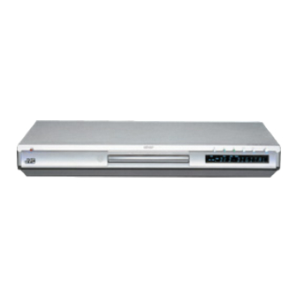
SERVICE MANUAL
DVD VIDEO PLAYER
TV
DVD
STANDBY/ON
OPEN/
CLOSE
TV
DVD
TV1
TV2
TV3
1
2
3
TV4
TV5
TV6
4
5
6
TV7
TV8
TV9
7
8
9
TV-/--
TV0
MUTING
10
0
+10
TITLE/
TV/VIDEO
RETURN
SUBTITLE
GROUP
CANCEL
CH
+
VOL-
VOL+
ENTER
CH
-
PREVIOUS
NEXT
CLEAR
SELECT
STROBE
SLOW -
SLOW+
REPEAT
SUB TITLE
AUDIO
VFP
DIGEST
ANGLE
ZOOM
3D
PHONIC
AMP VOL
RM-SXV010U
REMOTE CONTROL
COPYRIGHT
XV-N5SL
XV-N5 DVD/SUPER VCD/VCD/CD PLAYER
For only ver.UG,US,UW,UB
2002 VICTOR COMPANY OF JAPAN, LTD.
XV-N5SL
Area Suffix
A -------------------- Australia
B -------------------------- U.K.
E --- Continental Europe
EN ---- Northern Europe
EV ------ Eastern Europe
EE -- Russian Federation
UG --------- Turkey,Egypt,
South Africa
US ------------- Singapore
UW --- Brazil,Mexico,Peru
UB ------------ Hong Kong
No.A0033
Jul. 2002
Advertisement
Table of Contents

Related Manuals for JVC XV-N5SL


Summary of Contents for JVC XV-N5SL
- Page 1 XV-N5SL SERVICE MANUAL DVD VIDEO PLAYER XV-N5SL Area Suffix A -------------------- Australia B -------------------------- U.K. E --- Continental Europe EN ---- Northern Europe EV ------ Eastern Europe EE -- Russian Federation UG --------- Turkey,Egypt, South Africa US ------------- Singapore UW --- Brazil,Mexico,Peru...
-
Page 2: Table Of Contents
XV-N5SL TABLE OF CONTENTS Important Safety Precautions ............. 3 Safety Precautions . -
Page 3: Important Safety Precautions
XV-N5SL SECTION 1 Important Safety Precautions 1.1 Safety Precautions (1) This design of this product contains special hardware and voltmeter. many circuits and components specially for safety purposes. Move the resistor connection to each exposed metal part, For continued protection, no changes should be made to the... -
Page 4: Preventing Static Electricity
XV-N5SL 1.5 Preventing static electricity Electrostatic discharge (ESD), which occurs when static electricity stored in the body, fabric, etc. is discharged, can destroy the laser diode in the traverse unit (optical pickup). Take care to prevent this when performing repairs. -
Page 5: Important For Laser Products
XV-N5SL 1.7 Important for laser products (1) CLASS 1 LASER PRODUCT (5) CAUTION : If safety switches malfunction, the laser is able (2) DANGER : Invisible laser radiation when open and inter to function. lock failed or defeated. Avoid direct exposure to beam. -
Page 6: Precautions For Service
XV-N5SL 1.8 Precautions for Service 1.8.1 Handling of Traverse Unit and Laser Pickup (1) Do not touch any peripheral element of the pickup or the actuator. (2) The traverse unit and the pickup are precision devices and therefore must not be subjected to strong shock. -
Page 7: Disassembly Method
XV-N5SL SECTION 2 Disassembly method There is a part different from the photograph according to the model and the destination though explains this disassembly method by using version U.K. 2.1 Main body section 2.1.1 How to remove a top cover (See Figure 1) (1) Screw A attaches a top cover to the main part. - Page 8 XV-N5SL 2.1.3 How to remove a rear panel (See Figure 5 and 6) • Please remove a top cover before removing a rear panel. (1) Screw D attaches a rear panel to the main part. Remove the nine screws D.
- Page 9 XV-N5SL 2.1.5 How to remove a power supply board (See Figure 9 and 5) • Please remove a top cover before removing a power supply board. (1) Extract flat wire from connector JT911, JT912, and JT913 on a power supply board.
-
Page 10: Mechanism
XV-N5SL SECTION 3 Mechanism 3.1 Loading assembly section 3.1.1 Removing the clamper assembly (See Fig.1) (1) Remove the four screws A attaching the clamper assembly. (2) Move the clamper in the direction of the arrow to release the two joints a on both sides. - Page 11 XV-N5SL 3.1.3 Removing the traverse mechanism assembly (See Fig.4 and 5) • Prior to performing the following procedure, remove the clamper assembly and the tray. (1) Remove the four screws B attaching the traverse mechanism assembly. ATTENTION: Before reattaching the traverse...
- Page 12 XV-N5SL 3.1.5 Removing the motor assembly (See Fig.7 and 8) • Prior to performing the following procedure, remove the clamper assembly, the tray.the traverse mechanism assembly and the elevator. (1) Remove the belt from the pulley. (2) Remove the screw C attaching the motor assembly.
- Page 13 XV-N5SL Fig.9 3.1.6 Removing the Idle gear/pully gear/ middle gear/slitecam (See Fig.9 to 11) • Prior to performing the followong procedure,remove the clamper assembly,the tray,the traverse mechanism assembly,the elevator and the motor assembly. (1) Press the two tabs h inward and pull out idle gear.
-
Page 14: Traverse Mechanism Assembly Section
XV-N5SL 3.2 Traverse mechanism assembly section 3.2.1 Removing the feed motor assembly (See Fig.12) (1) Unsolder the two soldering j on the spindle motor board. (2) Remove the four screws F attaching the feed motor assembly. Fig.12 3.2.2 Removing the feed motor (See Fig.12 to 14) - Page 15 XV-N5SL 3.2.3 Removing the pickup (See Fig.16 and 18) (1) Remove the screw I attaching the T spring (S) and the shaft holder. Remove also the plate. ATTENTION: When reattaching,make sure that the T spring (S) presses the shaft. (2) Pull out the part l of the shaft upward. Move the part m in the direction of the arrow and detach from the spindle base.
- Page 16 XV-N5SL 3.2.5 Removing the spindle motor assembly (See Fig.19 to 21) (1) Remove the three screws L attaching the spindle motor on the bottom of the mechanism base. ATTENTION: When reattaching, pass the card wire extending from the spindle motor board through the notch of the spindle base.
-
Page 17: Adjustment Method
XV-N5SL SECTION 4 Adjustment method 4.1 Test mode setting method (1) Take out the disc and close the tray. (2) Unplug the power plug. (3) Insert power plug into outlet while pressing both "PLAY" key and "STOP" key of the main body. -
Page 18: Display Of Current Value Of Laser
XV-N5SL 4.4 Display of current value of laser (1) Makes to test mode and initializes. (2) When "CHOICE" key of remote controller is pushed four times, It is displayed on the LCD display, "CHECK". (3) Afterwards, the laser current value can be switched by pushing the key to remote controller without turning on the disc. -
Page 19: Upgrading Of Firmware
XV-N5SL 4.6 Upgrading of firmware (1) The power supply is turned on pushing the "POWER" key. (2) The up-grade disc is inserted. (3) When LCD display of the main body changes from "READING" into "UPGRADE", cursor "UP" key ( ) of remote controller is pushed. -
Page 20: Flap Adjustment Of The Pick-Up Guide Shaft
XV-N5SL 4.8 Flap adjustment of the pick-up guide shaft 4.8.1 Tool list for adjustment Hex wrench for adjustment Off-the-shelf (1.3mm) Test disc VT-501 or VT-502 Stand of about 150mm in height 2 pcs (1) Puts into the state to display the jitter value on the LCD display referring to "3.5 Display of the jitter value". -
Page 21: Attention When Pick-Up Is Exchanged
XV-N5SL 4.9 Attention when pick-up is exchanged (1) Flexible wire, pick-up spring, switch actuator, and lead spring are removed from an old pick-up (broken the one). < Guide > Flexible wire, pick-up spring and switch actuator,lead spring are removed without each decomposing while assembled. -
Page 22: Confirm Method Of Operation
The EEPROM is initialized. Refer to the initialization method. Opening picture check (Power ON) It should be display "JVC" Muting working The noise must not be had to the performance beginning when you push "PLAY" button or at ON/STANDBY. FL Display The mark and the logo, etc. -
Page 23: Troubleshooting
XV-N5SL 4.11Troubleshooting 4.11.1 Servo volume Fig.1... -
Page 24: Check Points For Each Error
XV-N5SL 4.12Check points for each error 4.12.1 Spindle start error (1) Defective spindle motor • Are there several ohms resistance between each pin of CN201 "5-6","6-7","5-7"? (The power supply is turned off and measured.) • Is the sign wave of about 100mVp-p in the voltage had from each terminal? [ CN201"9"(H1-),"10"(H1+),"11"(H2-),"12"(H2+),"13"(H3-),"14"(H3+) ]... - Page 25 XV-N5SL 4.12.3 Traverse movement NG (1) Defective traverse driver • Has the voltage come between terminal of CN101 "1" and "2" ? (2) Defective BTL driver (IC201) • Has the motor drive voltage gone out to IC201"17" or "18"? (3) Has the control signal come from servo IC or the microcomputer? •...
- Page 26 XV-N5SL 4.12.9 Neither picture nor sound is output (1) It is not possible search • Has the tracking been turned on? • To "(5) Tracking ON NG" in "Check points for each error" when the tracking is not normal. • Is the feed operation normal? To "(3) traverse movement NG"...
-
Page 27: Description Of Major Ics
XV-N5SL SECTION 5 Description of major ICs 5.1 74LCX373MTC-X(IC512,IC513) 5.1.2 Pin function 5.1.1 Pin layout Description Symbol Data inputs D0~D7 Latch enable input Output enable input 3-State latch outputs Q0~Q7 5.1.3 Truth table INPUTS OUTPUTS H = HIGH Voltage level... -
Page 28: Ba5983Fm-X (Ic201) : 4Ch Driver
XV-N5SL 5.2 BA5983FM-X (IC201) : 4CH Driver 5.2.1 Block diagram 5.2.2 Pin function Pin No. Symbol Description Pin No. Symbol Description BIAS IN Input for Bias-amplifier VO4(-) O Inverted output of CH4 OPIN1(+) Non inverting input for CH1 OP-AMP VO3(+) -
Page 29: An8703Fh-V (Ic101) : Frontend Processor
XV-N5SL 5.3 AN8703FH-V (IC101) : Frontend processor 5.3.1 Pin layout 5.3.2 Pin function Pin No. Symbol Description Pin No. Symbol Description LPC1 I Laser input terminal (DVD) RFDIFO - Non connect LPC01 O Laser drive signal output terminal (DVD) RFOUT... -
Page 30: Ba6664Fm-X (Ic251) : 3Phase Motor Driver
XV-N5SL 5.4 BA6664FM-X (IC251) : 3Phase Motor Driver 5.4.1 Pin layout 5.4.2 Block diagram... - Page 31 XV-N5SL 5.4.3 Pin function (BA6664FM-X) Pin No. Symbol Description Non connect Output 3 for spindle motor Non connect Output 2 for spindle motor Non connect Non connect Output 1 for spindle motor Connect to ground Positive input for hall input AMP 1...
-
Page 32: K4S641632F-Tc75 (Ic506) :Cmos Sdram
XV-N5SL 5.5 K4S641632F-TC75 (IC506) :CMOS SDRAM 5.5.1 Pin layout 5.5.2 Block diagram 5.5.3 Pin functions Symbol Description System clock Chip select Clock enable A0~A11 address BS0,1 Bank address strobe Row address strobe column address strobe Write enable LDQM Data input/output mask... -
Page 33: Mn101C57Dlr(Ic1):System Controller
XV-N5SL 5.6 MN101C57DLR(IC1):System controller 5.6.1 Pin function Pin No. Symbol Description VLC1 LCD Power supply terminal 1 (B5V) VLC2 LCD Power supply terminal 2 (B5V divide voltage) VLC3 LCD Power supply terminal 3 (B5V divide voltage) Non connect P.ON Indicator control signal output for STANDBY... -
Page 34: Mm1565Af-X (Ic951) : 500Ma Regulator
XV-N5SL 5.7 MM1565AF-X (IC951) : 500mA Regulator 5.7.1 Block diagram 5.7.2 Pin function Pin No. Symbol Function Vout Output terminal Non connect Connect to ground Noise decrease terminal Cout Control terminal Substrate (Connect to ground) Input terminal... -
Page 35: Mn102L62Glf3 (Ic401) : Unit Cpu
XV-N5SL 5.8 MN102L62GLF3 (IC401) : Unit CPU 5.8.1 Pin function Pin No. Symbol Function Pin No. Symbol Function WAIT Micon wait signal input SWUPDN Non connect Read enable MECHA_H/V Connect to ground SPMUTE Spindle muting output to IC251 DISCSET Mechanism state signal input... -
Page 36: Mn103S26Ega (Ic301) : Super Optical Disc Controller
XV-N5SL 5.9 MN103S26EGA (IC301) : Super optical disc controller 5.9.1 Terminal layout 5.9.2 Block diagram 5.9.3 Pin function (1/4) Pin No. Symbol Description NINT0,1 Interruption of system control 0,1 VDD3 Power supply terminal for I/O(3.3V) Connect to ground NINT2 Interruption of system control 2... - Page 37 XV-N5SL 5.9.4 Pin function (MN103S28EGA : 2/4) Pin No. Symbol Description Read signal input from system controller 37~44 CPUDT7~0 System control data CLKOUT1 Non connect MMOD Test mode switch signal NRST System reset MSTPOL Master terminal polarity switch input SCLOCK...
- Page 38 XV-N5SL 5.9.5 Pin function (MN103S28EGA : 3/4) Pin No. Symbol Description PLFLT1 Connect to capacitor 1 for PLL AVSS Connect to ground for analog circuit Connect to resistor for VREF reference current source VREFH Reference voltage input (2.2V) PLPG Non connect VHALF Reference voltage input (1.65V)
- Page 39 XV-N5SL 5.9.6 Pin function (MN103S28EGA : 4/4) Pin No. Symbol Description Connect to ground VDD3 Power supply terminal for I/O (3.3V) HDD1 ATAPI host data 1 HDD13 ATAPI host data 13 HDD2 ATAPI host data 2 HDD12 ATAPI host data 12...
-
Page 40: Mn35505-X (Ic703) : Dac
XV-N5SL 5.10 MN35505-X (IC703) : DAC 5.10.1 Terminal layout 5.10.2 Pin function Pin No. Symbol Description Control signal for DAC Digital data input LRCK L and R clock for DAC Bit clock for DAC Control signal for DAC DVDD2 Power supply terminal... -
Page 41: Ndv8601Vwa-Be(Ic501):Av Decoder
XV-N5SL 5.11 NDV8601VWA-BE(IC501):AV Decoder 5.11.1 Pin layout 5.11.2 Block diagram 5.11.3 Pin function (1/4) Pin No. Symbol Description VDDio Power supply terminal 3.3V MD10,11 I/O SDRAM Data bus terminal Power supply terminal 1.8V MD12 I/O SDRAM Data bus terminal VSSio... - Page 42 XV-N5SL 5.11.4 Pin function (NDV8601VWA-BE 2/4) Pin No. Symbol Description MA11 Non connect VSSio Connect to ground 32,33 MA12,13 SDRAM Address bus, reserved for terminal compatibility with 64Mb SDRAM Power supply terminal 1.8V SDRAM Primary bank chip select VDDio Power supply terminal 3.3V...
- Page 43 XV-N5SL 5.11.5 Pin function (NDV8601VWA-BE 3/4) Pin No. Symbol Description VDDio Power supply terminal 3.3V SSPOUT0 I/O SSP0 Data out or UART0 data-terminal-ready signal TXD0 I/O UART0 Serial data output to an external serial device RXD0 UART0 Serial data input from external serial device...
- Page 44 XV-N5SL 5.11.6 Pin function (NDV8601VWA-BE 4/4) Pin No. Symbol I/O Description SCLK External bus clock used for programmable host peripherals I/O Programmable WAIT/ACK/RDY control VSSio Connect to ground 163~168 AD13~8 I/O Multiplexed address / data bus terminal VDDio Power supply terminal 3.3V...
-
Page 45: S-93C66Afj-X (Ic451,Ic510) : Eeprom
XV-N5SL 5.12 S-93C66AFJ-X (IC451,IC510) : EEPROM 5.12.1 Pin layout 5.12.2 Pin function Pin No. Symbol I/O Description Non connect Power supply terminal Chip select input Serial clock input Serial data input Serial data output Connect to ground Non connect 5.12.3 Block diagram... -
Page 46: Sst39Vf160-7Cek (Ic509) : 16M Eeprom
XV-N5SL 5.13 SST39VF160-7CEK (IC509) : 16M EEPROM 5.13.1 Pin layout 5.13.2 Block diagram 5.13.3 Pin function Symbol Pin name Function A19~A0 Address Inputs To provide memory addresses. During sector erase A19~A11 address lines will select the sector. During block erase A19~A15 address lines will select the block. -
Page 47: Str-G6551-F8 (Ic901) : Switch Regulator
XV-N5SL 5.14 STR-G6551-F8 (IC901) : Switch regulator 5.14.1 Block diagram 5.14.2 Pin function Pin No. Symbol Description Function Drain terminal MOS FET drain Source terminal MOS FET source Ground terminal Ground Power supply terminal Input of power supply for control circuit O.C.P/F.B... -
Page 48: Glossary Of Term And Abbreviations(For Av Decoder Section)
XV-N5SL SECTION 6 Glossary of term and abbreviations(for AV Decoder section) 3-dimension 1)audio/video 2)audio/visual alternating current ACLK audio serial-data (bit) clock multiplexed address / data bus analog-to-digital converter digital audio input address latch enable ANSI/SMPTE American National Standards Institute / Society of Motion Pictures and Television Engineers... - Page 49 XV-N5SL MCLK primary or master clock Megahertz MIPS Million Instructions Per Second MmCPU Mediamatics CPU (synonym for internal RISC CPU) Moving Picture Experts Group Layer-3 Audio (audio file format / extension) MPEG1 audio A digital audio format mainly used in video CDs. It is based on the moving picture expert group (MPEG1) format, a data compression technology.
- Page 50 XV-N5SL VICTOR COMPANY OF JAPAN, LIMITED PERSONAL & MOBILE NETWORK BUSINESS UNIT 1644, Shimotsuruma, Yamato, Kanagawa 242-8514, Japan 200207 No.A0033...
- Page 51 XV-N5SL In regard with component parts appearing on the silk-screen printed side (parts side) of the PWB diagrams, the parts that are printed over with black such as the resistor ( diode ( ) and ICP ( ) or identified by the " " mark nearby are critical for safety.
- Page 52 XV-N5SL Block diagrams DVD Servo control & AV decoder section (SHEET 1,2,3) CN511 FW901 FW903 CN101 CN201 CN202...
- Page 53 XV-N5SL DAC & Audio signal output section (SHEET 5) MUTE LMMUTE MUTE SHEET 3 Front audio OUT1C Q705,Q791 AOUT0 IC741,IC751 OUT1D DCLK LRCK IC703 OUT2C DAC0SC DDATA OUT2D Q743 Front analog audio OUT LCH RCH Q753 J700 MUTE2 SHEET 4...
- Page 54 XV-N5SL Power supply section (SHEET 7) TO CN801 SHEET 4 J902 CN902 J901 R/C,G,B,CV/Y COMPULINK AC-DC D956 AVCOMP Q910 C982,C984 Q911 LCH,RCH,MUTE2 L957 -12V AC-DC Line filter AC-DC D957 AC IN +12V C987,C989 L901 D901 L959 TO FW903 SHEET 3...
- Page 55 XV-N5SL Standard schematic diagrams Servo control section S3.3V D3.3V D1.8V K301 NQR0007-002X K302 NQR0007-002X K303 NQR0007-002X R341 5.6K C144 0.01/16 C145 CN101 QGF0523F1-30W DGND TO SHEET 2 T2CD HDTYPE F2CD ODCIRQ2 R318 ODCIRQ R319 C347 T1CD C141 TP309 0.1/16 0.1/16...
- Page 56 XV-N5SL AV Decoder section D3.3V R998 R995 D1.8V D3.3V TO SHEET 3 C521 K504 NQR0007-002X K503 R505 TO SHEET 1 R506 R507 C527 C524 47/4 47/4 D3.3V R508 K501 NQR0007-002X PWE0 IC505 W986432DH-7 C511 C512 0.1/16 47/4 IC506 MD10 K4S641632F-TC75...
- Page 57 XV-N5SL Flash ROM section D3.3V TO SHEET 2 C504 C500 100/10 C593 C590 100/10 EP701 C579 QNZ0136-001Z DGND S3.3V L503 L502 +12V -12V R510 C505 C502 C594 100/10 C591 100/10 FW901 QUM108-14DGZ4 D3.3V D3.3V P.ON SGND JT911,JT912 D3.3V LADD16 SHEET 7...
- Page 58 XV-N5SL Video signal output section R842 R823 R819 R820 2.2K R821 9.1K Q821 R824 KRC102S-X R822 9.1K R825 K801 K802 NQR0007-002X NQR0007-002X Q822 KRC102S-X C820 J800 QNZ0499-001 C851 J801 100/10 R800 IC801 MM1568AJ-X R828 TO SHEET 2 R870 C853 R829...
- Page 59 XV-N5SL DAC & audio signal output section R795 Q828 KRA121S-X R794 Q705 KRA102S-X R1500 R742 C745 Q791 0.01 2SC2412K/RS/-X C700 C741 R726 220/10 R746 K703 R743 C761 Q704 NQR0007-002X 3.3k C710 R729 KRC109S-X R731 0.001 3.3k R761 R748 C746 R765...
- Page 60 XV-N5SL System control & LCD display section QLD0239-001 QGF1016C1-13 QGF1016F3-13 KRA103S-X KRC107S-X QSW0651-001Z QGF1016C1-27 47/10 B3.3V KRC107S-X GP1UD271XK SWUPDN 0.022 SWOPEN /LMMUTE TCLOSE TOPEN XC61FN2712M-X SELU2E10C 4.7K TO CN511 4.7K SHEET 3 0.01 SEG21 CPURST SEG22 QAX0667-001Z SEG23 MUTE SEG24...
- Page 61 XV-N5SL Power supply section BK901 R951 R909 R952 R953 C910 Q910 R912 2SC3576-JVC-T R954 22/25 R914 R916 R917 J902 QNZ0516-001 R915 C911 R913 Q911 22/25 2SC3576-JVC-T TO CN801 SHEET 4 L959 D957 F1T4-T2 180/25 470/16 CN902 C987 C989 QGF1205C1-15 180/25...
- Page 62 XV-N5SL Printed circuit boards Servo control & output terminal board (Forward side) K573 R1525 IC522 IC510 CN202 K572 C123 CN201 K576 C120 CN511 C117 R125 C122 C524 CN101 R124 R512 C809 C804 R506 R508 C118 C119 Q808 R806 R126 R803...
- Page 63 XV-N5SL Servo control & output terminal board (Reverse side) TP34 C206 K518 C263 C209 R207 C260 R204 TP510 C204 R203 R206 TP48 TP46 C207 TP43 C253 TP102 IC251 R220 TP49 TP501 R117 TP525 R210 TP18 TP519 K579 C214 TP19 TP23...
- Page 64 XV-N5SL System control & power supply board C921 FC902 FC901 C905 R920 EP901 C907 R907 R908 R906 CN12 C915 C983 R901 PC901 C922 R969 IC951 C909 D904 C991 C981 R903 C968 C972 C969 D998 T901 R992 K904 R991 D908 D954...
- Page 65 XV-N5SL Loading motor board 2-15...
- Page 66 XV-N5SL PARTS LIST [XV-N5SL] * All printed circuit boards and its assemblies are not available as service parts. Area Suffix B ------ U.K. E ------ Continental Europe EN ---- Northern Europe EE ---- Russian Federation EV ---- Eastern Europe A ------ Australia...
- Page 67 XV-N5SL Exploded view of general assembly and parts list Block No. M 26 BACK SIDE Grease JVS-1003 25 BACK SIDE...
- Page 68 XV-N5SL Parts list (General assembly) Block No. M1MM Item Parts number Parts name Q'ty Description Area LE10272-003A FRONT PANEL 1 except EUROPE A,UB,UG,US,UW LE10272-002A FRONT PANEL 1 EUROPE B,E,EE,EN,EV E75896-001 FELT SPACER 2 FRONT FOOT LE20638-005A WINDOW SCREEN LE20639-004A PUSH BUTTON...
- Page 69 XV-N5SL Parts list (General assembly) Block No. M1MM Item Parts number Parts name Q'ty Description Area QYSBSGY3008M SPECIAL SCREW 2 21P OUT QMF51E2-1R6-J1 FUSE QHS3771-108 CORD STOPPER QMPG070-244-JC POWER CORD QMPN160-200-JD POWER CORD B,UB QMPK190-200-JC POWER CORD E,EE,EN,EV,UG,US,UW QZW0004-001 WIRE CLAMP...
- Page 70 XV-N5SL DVD Traverse mechanism assembly and parts list Block No. M Grease EBS0006-013B PG-641 CFD-4007ZY2 12.0mm 0.2mm 65.2mm...
- Page 71 XV-N5SL Parts list (DVD Traverse mechanism assembly) Block No. M2MM Item Parts number Parts name Q'ty Description Area LE20520-002A MECHA BASE LE20516-001A SPINDLE BASE QYSDST2605M TAPPING SCREW LE30909-001A HOLDER QAR0165-001 FEED MOTOR LV41510-001A FEED GEAR QYSPSPU2040M SCREW LV41512-001A FEED GEAR...
- Page 72 XV-N5SL DVD Loading mechanism assembly and parts list Block No. M Grease UD-24H2 EM-30L CFD-4007ZY2 To G of Servo control & A/V output terminal board. To F of Servo control & A/V output terminal board.
- Page 73 XV-N5SL Parts list (DVD Loading mechanism assembly) Block No. M3MM Item Description Parts number Parts name Q'ty Area LV10454-007A LOADING BASE QAR0164-001 MOTOR LV42087-001A MOTOR PULLEY QYSPSPU1730Z SCREW VKZ4777-003 MINI SCREW LV42209-001A BELT LV42084-002A PULLEY GEAR LV42085-002A MIDDLE GEAR LV42086-001A...
- Page 74 XV-N5SL Electrical parts list (Servo control board) Block No. 01 Item Parts number Parts name Remarks Area Item Parts number Parts name Remarks Area C 105 NEA70JM-476X E.CAPACITOR C 315 NCB31HK-471X C CAPACITOR C 106 NEA70JM-476X E.CAPACITOR C 316 NCB31HK-271X...
- Page 75 XV-N5SL Electrical parts list (Servo control board) Block No. 01 Item Parts number Parts name Remarks Area Item Parts number Parts name Remarks Area C 531 NCB31CK-104X C CAPACITOR C 772 QETN1CM-107Z E CAPACITOR 100MF 20% 16V C 532 NCB31CK-104X...
- Page 76 XV-N5SL Electrical parts list (Servo control board) Block No. 01 Item Parts number Parts name Remarks Area Item Parts number Parts name Remarks Area IC801 MM1567AJ-X Q 826 DTC114EKA-X TRANSISTOR B,E,EN,EE,EV J 700 QNN0420-001 PIN JACK FRONT L/R Q 828 KRA121S-X DIGITAL.TR...
- Page 77 XV-N5SL Electrical parts list (Servo control board) Block No. 01 Item Parts number Parts name Remarks Area Item Parts number Parts name Remarks Area R 309 NRSA63J-473X MG RESISTOR R 589 NRSA63J-0R0X MG RESISTOR R 313 NRSA63J-473X MG RESISTOR R 655...
- Page 78 XV-N5SL Electrical parts list (Servo control board) Block No. 01 Item Parts number Parts name Remarks Area Item Parts number Parts name Remarks Area A,UB,UG,US,UW R 831 NRSA63J-0R0X MG RESISTOR R1518 NRSA63J-100X MG RESISTOR B,E,EN,EE,EV R 832 NRSA63J-0R0X MG RESISTOR...
- Page 79 XV-N5SL Electrical parts list (Main board) Block No. 02 Item Remarks Item Parts number Parts name Remarks Area Parts number Parts name Area BK901 E409182-001SM GRAND TERMINAL D 12 1SS355-X DIODE C.M NCS31HJ-331X C.CAPA. C.M D 13 1SS355-X DIODE C.M...
- Page 80 XV-N5SL Electrical parts list (Main board) Block No. 02 Item Parts number Parts name Remarks Area Item Parts number Parts name Remarks Area R 14 NRSA63J-222X MG RESISTOR QSW0651-001Z TACT SWITCH FW SKIP R 15 NRSA63J-103X MG RESISTOR T 901...
- Page 81 XV-N5SL Packing materials and accessories parts list Block No. M4MM Block No. M5MM Accessories A1~ A9,A11,A12 3-16...
- Page 82 XV-N5SL Parts list (Packing) Block No. M4MM Item Parts number Parts name Q'ty Description Area LE31032-009A PACKING CASE LE31032-020A PACKING CASE LE31032-007A PACKING CASE LE31032-019A PACKING CASE E,EN,EV LE31032-021A PACKING CASE LE31032-005A PACKING CASE LE31032-006A PACKING CASE LE31032-008A PACKING CASE...
Need help?
Do you have a question about the XV-N5SL and is the answer not in the manual?
Questions and answers