Table of Contents
Advertisement
Advertisement
Chapters
Table of Contents
Troubleshooting

Related Manuals for LG S92T2-C


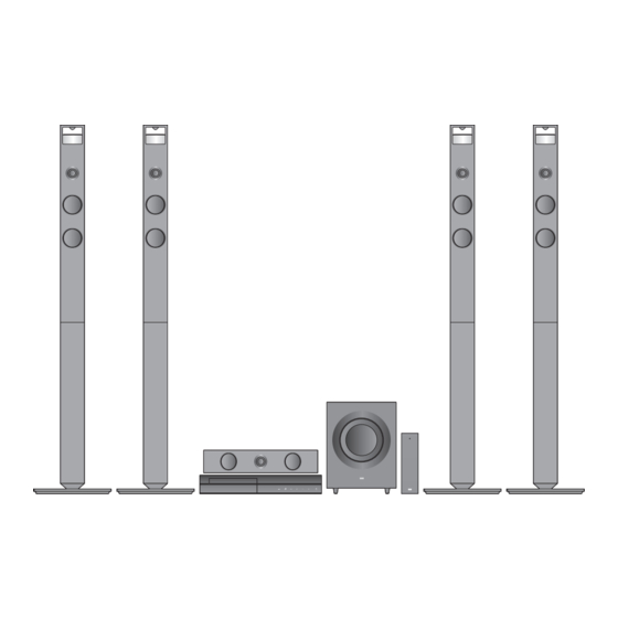
Summary of Contents for LG S92T2-C
- Page 1 Internal Use Only Website http://biz.lgservice.com CINEMA 3D SOUND Blu-ray HOME THEATER SYSTEM SERVICE MANUAL MODEL: BH9520TW (BH9520TW, S92T1-S/W, S92T1-C, T2, W2) CAUTION BEFORE SERVICING THE UNIT, READ THE “SAFETY PRECAUTIONS” IN THIS MANUAL. P/NO : AFN75741110 MARCH, 2012...
- Page 2 CONTENTS SECTION 1 ..SUMMARY SECTION 2 ..ELECTRICAL SECTION 3 ..CABINET & MAIN CHASSIS SECTION 4 ..MT8560 F/E LOADER PART SECTION 5 ..WIRELESS RECEIVER PART SECTION 6 ..REPLACEMENT PARTS LIST...
-
Page 3: Table Of Contents
SECTION 1 SUMMARY CONTENTS PRODUCT SAFETY SERVICING GUIDELINES FOR BD-HTS PRODUCTS ..........1-3 SERVICING PRECAUTIONS .......................... 1-4 • GENERAL SERVICING PRECAUTIONS • INSULATION CHECKING PRODEDURE • ELECTROSTATICALLY SENSITIVE (ES) DEVICES INITIAL SYSTEM SETUP ..........................1-5 HIDDEN KEY MODE ............................1-6 SOFTWARE UPGRADE .......................... -
Page 4: Product Safety Servicing Guidelines For Bd-Hts Products
When servicing this product, under no circumstances should the original design be modified or altered without permission from LG Corporation. All components should be replaced only with types identical to those in the original circuit and their physical location, wiring and lead dress must conform to original layout upon completion of repairs. -
Page 5: Servicing Precautions
SERVICING PRECAUTIONS CAUTION: Before servicing the BD-HTS covered by this ser- Electrostatically Sensitive (ES) Devices vice data and its supplements and addends, read and follow Some semiconductor (solid state) devices can be damaged the SAFETY PRECAUTIONS. easily by static electricity. Such components commonly are NOTE: if unforeseen circumstances create conflict between called Electrostatically Sensitive (ES) Devices. -
Page 6: Initial System Setup
INITIAL SYSTEM SETUP When you turn on the unit for the fi rst time, the initial setup wizard appears on the screen. Set the display language, network setting and speaker setup on the initial setup wizard. 1. Press (POWER). The initial setup wizard appears on the screen. 2. -
Page 7: Hidden Key Mode
HIDDEN KEY MODE HIDDEN AVAILABLE ENTRANCE EXIT DISPLAY MODE STATUS (NO DISC || OPEN) DISPLAY PAUSE or HOME SYSTEM && (Highlight on 1+3+9+7+1+3+9+ SYSTEM ※ ‘Pause’ Key INFORMATION 16:9 Full of setup ENTER or MP2 INFORMATION FACTORY RESET (KEY,VERSION) menu) 1. -
Page 8: Software Upgrade
SOFTWARE UPGRADE • Burn a DVD recordable disc or USB with a file that is named to “LG_HB_7000M60.ROM”. • Insert a upgrading disc or USB. • Show help message for disc upgrade as follows. Press Enter key to upgrade. Press Enter key to upgrade and it will show progress information. After completing upgrade then power is off. -
Page 9: Network Update
NETWORK UPDATE You can update the fi rmware by connecting your unit device directly to the S/W update server. Confi guring Network Settings To update the fi rmware by connecting your player directly to the S/W update server, your player must be connected to network. - Page 10 If newer version exists, 5) If newer version exists, the message “A new update was found. Do you want to download it?” appears. Select OK to download the update. (Selecting CANCEL will end the update.) 6) The player starts downloading the newest update from the SBP server.
-
Page 11: Specifications
SPECIFICATIONS • GENERAL Power requirements Refer to main label on the rear panel. Power consumption Refer to main label on the rear panel. Dimensions (W x H x D) Approx. 440 X 65 X 297 mm Net Weight (Approx.) 3.3 kg Operating temperature 5 °C to 35 °C (41 °F to 95 °F) Operating humidity... - Page 12 • SPEAKERS Front speaker (Left/ Right) Type 2 Way 3 speaker Impedance Rated 4 Ω Input Power 140 W Max. Input power 280 W Net Dimensions (W x H x D) 280 x 1 330 x 280 mm Net Weight 5.5 kg Rear speaker (Left/ Right) Type...
- Page 13 MEMO 1-12...
- Page 14 SECTION 2 ELECTRICAL CONTENTS DIGITAL DISPLAY & MEDIA TRAINING MASTER ......................2-2 1. DISTORTED PICTURE .............................. 2-2 2. NO PICTURE ................................2-7 3. PICTURE COLOR ..............................2-12 4. NOISE/AUDIO PROBLEMS ............................. 2-14 5. MISCELLANEOUS ..............................2-17 6. BLU-RAY PLAYER ..............................2-26 ONE POINT REPAIR GUIDE ..............................
-
Page 15: Digital Display & Media Training Master
DIGITAL DISPLAY & MEDIA TRAINING MASTER Objective: To provide clear and concise guidelines for customer service agents to handle calls on box goods calls. 1. DISTORTED PICTURE 1-1. Lines on Picture Distorted picture refers to the customer getting video, but there is a problem with the video. Determine what cables the customer is using to connect What cables is the BD to the TV and if connected properly. - Page 16 DIGITAL DISPLAY & MEDIA TRAINING MASTER 1-2. Ghost Picture Distorted picture refers to the customer getting video, but there is a problem with the video. Determine what cables the customer is using to connect the BD to the TV and if connected properly. Refer to OM for connections. What cables is the customer Tighten any loose cables.
- Page 17 DIGITAL DISPLAY & MEDIA TRAINING MASTER 1-3. Rolling Picture Distorted picture refers to the customer getting video, but there is a problem with the video. Determine what cables the customer is using to connect the BD to the TV and if connected properly. Refer to OM for connections. What cables is the customer Tighten any loose cables.
- Page 18 DIGITAL DISPLAY & MEDIA TRAINING MASTER 1-4. Shaky Picture Distorted picture refers to the customer getting video, but there is a problem with the video. Determine what cables the customer is using to connect the BD to the TV and if connected properly. Refer to OM for connections. What cables is the customer Tighten any loose cables.
- Page 19 DIGITAL DISPLAY & MEDIA TRAINING MASTER 1-5. Blurry Picture Distorted picture refers to the customer getting video, but there is a problem with the video. Determine what cables the customer is using to connect the BD to the TV and if connected properly. Refer to OM for connections. What cables is the customer Tighten any loose cables.
-
Page 20: Picture
DIGITAL DISPLAY & MEDIA TRAINING MASTER 2. NO PICTURE 2-1. Black Screen The entire screen is black. In case of customer use composite cable please make sure selecting Does the BD on-screen available resolution in the menu of the BD player, composite video can just menu appear? support 480i/p. - Page 21 DIGITAL DISPLAY & MEDIA TRAINING MASTER 2-2. Blue Screen The entire screen is a solid blue color. In case of customer use composite cable please make sure selecting Does the BD on-screen available resolution in the menu of the BD player, composite video can just menu appear? support 480i/p.
- Page 22 DIGITAL DISPLAY & MEDIA TRAINING MASTER 2-3. Snowy Screen A snowy picture is when black and white dots are all over the screen. In case of customer use composite cable please make sure selecting Does the BD on-screen available resolution in the menu of the BD player, composite video can just menu appear? support 480i/p.
- Page 23 DIGITAL DISPLAY & MEDIA TRAINING MASTER 2-4. No Signal A “no signal” message appears on the screen of the display. In case of customer use composite cable please make sure selecting Does the BD on-screen available resolution in the menu of the BD player, composite video can just menu appear? support 480i/p.
- Page 24 DIGITAL DISPLAY & MEDIA TRAINING MASTER 2-5. Invalid Format or Format Not Supported Make sure the customer’s simultaneously connecting analog component cable with HDMI cable. And then If Copy Protected Disc is playing back, Is the customer using a analog component output is no picture. Only when the analog output digital cable connection? is 480i, you can see the picture.
-
Page 25: Picture Color
DIGITAL DISPLAY & MEDIA TRAINING MASTER 3. PICTURE COLOR 3-1. No Color The video displays no color and only shows in black and white. Determine what cables the customer is using to connect the BD What cables is the customer to the TV and if connected properly. - Page 26 DIGITAL DISPLAY & MEDIA TRAINING MASTER 3-2. Poor Color The color is poor. Examples would be washed out colors, colors bleeding into one another, or a solid tint to a screen. Determine what cables the customer is using to connect the BD to What cables is the customer the TV and if connected properly.
-
Page 27: Noise/Audio Problems
DIGITAL DISPLAY & MEDIA TRAINING MASTER 4. NOISE/AUDIO PROBLEMS 4-1. No Audio The customer is not able to get audio. Determine what cables the customer is using to connect the BD to the TV and if connected properly. Refer to OM for connections. What cables is the customer Tighten any loose cables. - Page 28 DIGITAL DISPLAY & MEDIA TRAINING MASTER 4-2. Distorted Audio The audio sounds muffled, scratchy, or the audio skips. Determine what cables the customer is using to connect the BD to the TV and if connected properly. Refer to OM for connections. What cables is the customer Tighten any loose cables.
- Page 29 DIGITAL DISPLAY & MEDIA TRAINING MASTER 4-3. Humming/Clicking Noise The unit is making a humming noise or a clicking noise. BD’s make a slight hum when playing discs. Does the noise only A clicking noise or a noise interfering with audio may indicate a problem. happen when a disc Try multiple discs.
-
Page 30: Miscellaneous
DIGITAL DISPLAY & MEDIA TRAINING MASTER 5. MISCELLANEOUS 5-1. No Power The unit will not turn on. Is the unit plugged in? Is the unit plugged in? Does the unit turn on See if the unit will turn on when the power button the unit is pressed. when the power button If the unit turns on, then troubleshoot the remote control using is pressed on the unit? - Page 31 DIGITAL DISPLAY & MEDIA TRAINING MASTER 5-2. Disc Error The unit displays “disc error” when a disc is inserted into the BD player. Is the disc inserted into Make sure the disc has been inserted into the BD player properly. the BD player properly? The player can not read a disc inserted into the unit upside down.
- Page 32 DIGITAL DISPLAY & MEDIA TRAINING MASTER 5-3. Unit Locks Up Unit does not respond to any commands. If the unit will turn on or off with the button on the unit, Does the unit respond to troubleshoot the remote control. Please refer to the buttons on the unit? Remote Control Not Working call flow.
- Page 33 Please refer to the OM for instructions on how to program remote to TV. Customer wants to program a remote Does the customer want to other than Zenith or LG, the customer will need to contact program their remote? the manufacturer of the remote control. Codes do not work, remote is not compatible.
- Page 34 DIGITAL DISPLAY & MEDIA TRAINING MASTER 5-6. Will Not Play Disc The unit will not play a disc when a disc is inserted into the player. Is the disc inserted into Make sure the disc has been inserted into the BD player properly. the BD player properly? The player can not read a disc inserted into the unit upside down.
- Page 35 DIGITAL DISPLAY & MEDIA TRAINING MASTER 5-7. Disc Freezes or Skips The audio and video freeze and skip during play back of a BD or DVD disc. Is the disc inserted into Make sure the disc has been inserted into the BD player properly. the BD player properly? The player can not read a disc inserted into the unit upside down.
- Page 36 DIGITAL DISPLAY & MEDIA TRAINING MASTER 5-8. Can Access Menu, but Not Play a Movie The disc menu is displayed but the disc will not play. Go into the system information screen of the BD player. To access this menu, bring up the main menu. Go to TV aspect, Check the system information highlight 16:9, press 1397139 and hit enter.
- Page 37 DIGITAL DISPLAY & MEDIA TRAINING MASTER 5-10. Aspect Ratio The customer has bars on the top and bottom of the screen, the left and right of the screen, or both. A full screen movie played on a wide screen TV will have bars Is the movie on the left and right side of the TV.
- Page 38 DIGITAL DISPLAY & MEDIA TRAINING MASTER 5-11. My Unit Won’t be up-converted The customer has a problem with getting the unit to change resolutions to 480i/p, 720i/p, 1080i, or 1080p. Ask the customer to press stop to stop the disc from playing. Is the disc Ask the customer to press the resolution button to change the resolution.
-
Page 39: Blu-Ray Player
DIGITAL DISPLAY & MEDIA TRAINING MASTER 6. BLU-RAY PLAYER 6-1. Slow Loading Times for BD’s When a customer switches from one disc to another, Why does it take so long the lens have to be changed what causes the delay. to load my BD’s? BLU-RAY require different lasers to read the discs. -
Page 40: One Point Repair Guide
ONE POINT REPAIR GUIDE 1. NO POWER PROBLEM No power problem occurs when you power on the unit. 1-1. Fuse & Bridge diode 1-1-1. Solution Replace F901, BD901 on SMPS board. 1-1-2. How to troubleshoot (Countermeasure) 1) Look at the physical of fuse F901. 2) Check the bridge diode BD901. - Page 41 ONE POINT REPAIR GUIDE No power problem occurs when you power on the unit. 1-2. VFD, 14 VA, 6 VA, 3.8 VA 1-2-1. Solution Replace D922, D923, D924, D925, D926, D927, IC901. 1-2-2. How to troubleshoot (Countermeasure) Case 1) FLD abnormal: Check D926, D927, ZD951, ZD952, FR952 and replace it. Case 2) 6 VA abnormal: Check D924 and replace it.
-
Page 42: Booting When You Turn The Unit On, No Message Or "Welcome" On Front Panel
ONE POINT REPAIR GUIDE 2. NO BOOTING WHEN YOU TURN THE UNIT ON, NO MESSAGE OR “WELCOME” ON FRONT PANEL When you turn on your set, it will blank / no message on front panel, and stand-by led no working. 2-1. - Page 43 ONE POINT REPAIR GUIDE When you turn on your set, it will blank / no message or Welcome on front panel, and it will not boot-up. 2-2. IC151 (NO 3.3 V) 2-2-1. Solution Replace IC151 on MAIN board. 2-2-2. How to troubleshoot (Countermeasure) 1) Please check 3.8 VA of IC151 pin2 (VIN).
- Page 44 ONE POINT REPAIR GUIDE When you turn on your set, it will blank / no message or Welcome on front panel, and it will not boot-up. 2-3. IC150 (NO 1.5 V) 2-3-1. Solution Replace IC150 on MAIN board. 2-3-2. How to troubleshoot (Countermeasure) 1) Please check 1.5 V of IC150 on MAIN board.
- Page 45 ONE POINT REPAIR GUIDE When you turn on your set, it will blank / no message on front panel, and it will not boot-up. 2-4. IC155 (NO 1.2 V) 2-4-1. Solution Replace IC155 on MAIN board. 2-4-2. How to troubleshoot (Countermeasure) 1) Please check 1.2 V of IC155 on MAIN board.
- Page 46 ONE POINT REPAIR GUIDE When you turn on your set, it will display “WELCOME” on front panel, and it will not boot-up normally. 2-5. X501 2-5-1. Solution Replace X501 on MAIN board. 2-5-2. How to troubleshoot (Countermeasure) 1) Please check the soldering status of 27 MHz crystal (X501). 2) Please check the frequency of 27 MHz crystal (X501).
- Page 47 ONE POINT REPAIR GUIDE When you turn on your set, it will display “WELCOME” on front panel, and it will not boot-up normally. 2-6. IC504 (NAND FLASH MEMORY) 2-6-1. Solution Replace IC504 on MAIN board. 2-6-2. How to troubleshoot (Countermeasure) 1) Please check physical status of IC504 on your eyes.
- Page 48 ONE POINT REPAIR GUIDE When you turn on your set, it will display “WELCOME” on front panel, and it will not boot-up normally. 2-7. IC502, IC503 (DDR3 MEMORY) 2-7-1. Solution Replace IC502, IC503 on MAIN board. 2-7-2. How to troubleshoot (Countermeasure) 1) Please check 0.75 V of DDR3_VREF.
- Page 49 ONE POINT REPAIR GUIDE When you turn on your set, it will display “WELCOME” on front panel, and it will not boot-up normally. 2-8. IC501 (MPEG IC) 2-8-1. Solution Replace IC501 on MAIN board. 2-8-2. How to troubleshoot (Countermeasure) 1) Please check 1.2 V of C595 on MAIN board. Please check 3.3 V of C580 on MAIN board.
- Page 50 ONE POINT REPAIR GUIDE When you turn on your set, it will display “WELCOME” on front panel, and it will not boot-up normally. 2-9. MAIN BOARD 2-9-1. Solution Replace MAIN board. 2-9-2. How to troubleshoot (Countermeasure) 1) Please remove IC501 and IC502, IC503, IC504 and then check the Impedance between each signal (DATA, ADDRESS, and so on).
-
Page 51: Wired Network Connection Error
ONE POINT REPAIR GUIDE 3. WIRED NETWORK CONNECTION ERROR When you connect online service (like You-tube or Netflix2.1) through the wired LAN, the “no connection“ message appears. 3-1. JK250 (ETHERNET JACK) 3-1-1. Solution Replace JK250 on MAIN board. 3-1-2. How to troubleshoot (Countermeasure) 1) Check you internet connection. -
Page 52: Wireless Network Connection Error
ONE POINT REPAIR GUIDE 4. WIRELESS NETWORK CONNECTION ERROR When you connect online service (like You-tube or Netflix2.1) through the Wi-Fi, the “no connection“ message appears. 4-1. Wi-Fi MODULE 4-1-1. Solution Replace Wi-Fi module on FRONT panel. 4-1-2. How to troubleshoot (Countermeasure) 1) Check you internet connection. -
Page 53: Bad Hdmi Video / Audio Output
ONE POINT REPAIR GUIDE 5. BAD HDMI VIDEO / AUDIO OUTPUT When unit is connected to HDMI TV using HDMI cable, picture shows bad color, no output or mixed color on the screen. But component output is OK. 5-1. CN803 (HDMI JACK) 5-1-1. -
Page 54: Audio From Speaker
ONE POINT REPAIR GUIDE 6. NO AUDIO FROM SPEAKER When unit is connected to speaker, no audio from speaker. 6-1. IC602 (PWM IC) 6-1-1. Solution Replace IC602 (PWM IC). 6-1-2. How to troubleshoot (Countermeasure) 1) Check IC602 pin soldering. 2) If there is short soldering on pin IC602, re-soldering pin IC602. 3) If problem still occurs, check AMP IC (IC700, IC701, IC702, IC703). -
Page 55: Usb
ONE POINT REPAIR GUIDE 7. NO USB When unit is connected to USB, no audio and video from SET. 7-1. IC501 (MT8560) 7-1-1. Solution Replace IC501 (MT8560). 7-1-2. How to troubleshoot (Countermeasure) 1) Check CN202 connector and FFC cable. 2) If there is short soldering on CN202, re-soldering CN202. 3) If problem still occurs, check 5 V (CN202 pin4 ~ pin8). -
Page 56: Electrical Troubleshooting Guide
ELECTRICAL TROUBLESHOOTING GUIDE 1. SYSTEM POWER SUPPLY ON SMPS BOARD No 3.8 VA Replace F901 (same fuse). Is F901 normal? Replace TH901. Is TH901 normal ? Is BD901 normal? Replace BD901. Is the VCC Is D922 / D923 normal? (11 V ~ 25 V) supplied to IC901 pin4? Check or replace D922 / D923. - Page 57 ELECTRICAL TROUBLESHOOTING GUIDE No 6 VA Replace F901 (same fuse). Is F901 normal? Replace TH901. Is TH901 normal ? Is BD901 normal? Replace BD901. Is the VCC Is D924 normal? (11 V ~ 25 V) supplied to IC901 pin4? Check or replace D924. Power line of MAIN PCB is short.
- Page 58 ELECTRICAL TROUBLESHOOTING GUIDE No 14 VA Replace F901 (same fuse). Is F901 normal? Replace TH901. Is TH901 normal ? Is BD901 normal? Replace BD901. Is the VCC Is D925 normal? (11 V ~ 25 V) supplied to IC901 pin4? Check or replace D925. Power line of MAIN PCB is short.
-
Page 59: Amp Power Supply On Smps Board
ELECTRICAL TROUBLESHOOTING GUIDE 2. AMP POWER SUPPLY ON SMPS BOARD No 36 VA / 26 VA Check MICOM IC. Is the P-CTL normal? Is the VCC Is Q910 normal? (11 V ~ 25 V) supplied to IC902 pin7? Check or replace Q910. Replace IC902. -
Page 60: Power Supply On Main Board
ELECTRICAL TROUBLESHOOTING GUIDE 3. POWER SUPPLY ON MAIN BOARD No 3.3 V Is the Check 3.8 VA on SMPS board. VCC supplied to IC151 pin2? Is there Check IC101 pin58 (DCDC33_CTRL). signal at IC151 pin1? Check IC151 and replace. 3.3 VA (3.3VA_MICOM) Is D101 diode input Check 3.8 VA on MAIN board. - Page 61 ELECTRICAL TROUBLESHOOTING GUIDE No 12 V (12V_LOADER) Is the Check 14 VA on SMPS board. VCC supplied to IC156 pin2? Is there Check IC101 pin68 (LDO_CTRL). signal at IC156 pin1? Check IC156 and replace. No 9.5 V (A9P5V) Is the Check 14 VA on SMPS board.
- Page 62 ELECTRICAL TROUBLESHOOTING GUIDE No 5 V (5V_LOADER) Is the Check 6 VA on SMPS board. VCC supplied to IC703 pin2? Is there Check IC101 pin61 (PWR_CTRL). signal at IC703 pin1? Check IC703 and replace. No 1.8 V (DVDD18_TX / PVDD18_TX) IC801, IC806 HDMI Is the Check IC151 pin3 (VCC_3V3).
- Page 63 ELECTRICAL TROUBLESHOOTING GUIDE No 1.8 V (DSP VDD18) IC401 DSP Is the Check IC151 pin3 (VCC_3V3). VCC supplied to IC405 pin3? Check IC405 and replace. No 5 V (SYSTEM VCC_5V) Is the Check 6 VA on SMPS board. VCC supplied to IC153 pin2? Is there Check IC101 pin68 (LDO_CTRL).
- Page 64 ELECTRICAL TROUBLESHOOTING GUIDE No 5 V (MIC AVCC_5V) Is the Check 6 VA on SMPS board. VCC supplied to IC154 pin2? Is there Check IC101 pin68 (LDO_CTRL). signal at IC154 pin1? Check IC154 and replace. No 5 V (5V_IPOD / USB_5V) Is the Check 14 VA on SMPS board.
- Page 65 ELECTRICAL TROUBLESHOOTING GUIDE No 1.5 V Is the Check 14 VA on SMPS board. VCC supplied to IC150 pin13? Is there Check IC101 pin59 (DCDC15_CTRL). signal at IC150 pin15? Check IC150 and replace. No 1.2 V Is the Check 14 VA on SMPS board. VCC supplied to IC155 pin2? Is there...
-
Page 66: System Part
ELECTRICAL TROUBLESHOOTING GUIDE 4. SYSTEM PART Power on Check D101 Stand-by LED 3.3 VA, 3.8 VA and 3.8 VA on SMPS board. IC101: 3.3 VA / Check IC101 / IC150 / IC151 / IC150 : 1.5 V / IC151 : 3.3 V / IC155 and SMPS board. - Page 67 ELECTRICAL TROUBLESHOOTING GUIDE IC101: 3.3 VA / “LG Logo” Check IC101 / IC150 / IC151 / IC150 : 1.5 V / IC151 : 3.3 V / display on monitor IC155 and SMPS board. IC155 : 1.2 V OK? X501 27.000 MHz Replace X501.
-
Page 68: Cvbs Video Output
ELECTRICAL TROUBLESHOOTING GUIDE 5. NO CVBS VIDEO OUTPUT No CVBS / COMPOSITE video on display Is there Check IC501’s VCC CVBS signal or replace IC501. on L2V1? Is there Replace L2V1. CVBS signal out of L2V1? D201 Is there Check IC153. 5 V OK? signal on D201? Check JK251... -
Page 69: Hdmi Output
ELECTRICAL TROUBLESHOOTING GUIDE 6. NO HDMI OUTPUT No HDMI audio / video output IC801, IC806 Check VCC 3V3 & 1.8 V VCC 3V3 & 1.8 V IC802, IC803, IC151. IC101 HDMI_SDA, SCL, HDMI_RST Check IC101. CEC_RX&TX, HDMI_RX_INT CN803 pin18 Check VCC 5 V from IC153. VCC 5 V OK? CN803 pin19 HPD Check hot plug detect signal from TV. -
Page 70: Audio Output
ELECTRICAL TROUBLESHOOTING GUIDE 7. NO AUDIO OUTPUT No AUDIO output IC602 Check IC601 pin2 supply 3.8 VA and pin1. 3.3 V OK? X600 Replace X600. 19.2 MHz OK? Check IC101 IC602 pin4, 5, 6, 7, 8, 9 I2C data OK? and IC401 pin47, 48, 49, 51, 52, 54. -
Page 71: Waveforms
WAVEFORMS 1. SYSTEM PART - 1 IC501 MT8560 X-TAL 27 MHz 2-58... -
Page 72: System Part - 2 (System Memory)
2. SYSTEM PART - 2 (SYSTEM MEMORY) IC501 MT8560 BA0 IC501 MT8560 WE# IC501 MT8560 CAS# IC501 MT8560 CK 2-59... -
Page 73: Video Part (100% Full Color Bar)
3. VIDEO PART (100% FULL COLOR BAR) CVBS 2-60... -
Page 74: Audio Part - 1 (S/Pdif)
4. AUDIO PART - 1 (S/PDIF) CS8422_AUDIO_SPDIF IN 2-61... -
Page 75: Audio Part - 2 (I2S)
5. AUDIO PART - 2 (I2S) 2-62... -
Page 76: Hdmi Part
6. HDMI PART H_SDA H_SCL HDMI_CLK_N HDMI_0_N 2-63... - Page 77 MEMO 2-64...
-
Page 78: Wiring Diagram
WIRING DIAGRAM 24P FFC CABLE CN254 (MAIN – AMP) MAIN 14PIN HARNESS CABLE (MAIN – SMPS) CN251 8PIN B'd to B'd CN252 SMPS 18PIN FFC 8PIN FFC 5PIN HARNESS CABLE CABLE CABLE (MAIN – JACK) (MAIN – BT) (MAIN - Wi-Fi) : HARNESS 18PIN FFC CABLE... -
Page 79: Block Diagrams
BLOCK DIAGRAMS 1. OVERALL BLOCK DIAGRAM 1.2/3.3V 12C(1) 12C(1) 24.576 MHZ 3.3/5V 3.3V 12C(1) 32/12V Slave 3.3V Master Slave 3.3V TAS5624 SDRAM 150W Audio DSP 19.2 MHZ Portable CS495314 6ch ADC Flash CS8422 Tuner TAS5624 - Decoding CS5346 Bridge 150W - Processing SPDIF (D0~D3) -
Page 80: Smps #1 Block Diagram
2. SMPS #1 BLOCK DIAGRAM System TRANS Snubber Rectifier Power IC EER2828 & Smoothing IC Application Circuit (Bridge, CAPACITOR) Filter Section (Varistor, Resistor, Line Filter Thermistor) Digital TRANS Snubber AMP Power IC Power IC Application Circuit 2-69 2-70... -
Page 81: Smps #2 Block Diagram
3. SMPS #2 BLOCK DIAGRAM System TRANS Snubber Rectifier Power IC EER2828 & Smoothing IC Application Circuit (Bridge, Capacitor) Feedback AC INPUT (Varistor, Control Circuit Resistor, Line Filter Thermistor) TRANS Snubber AMP Power IC IC Application Circuit Feedback 2-71 2-72... -
Page 82: Audio Block Diagram
4. AUDIO BLOCK DIAGRAM VCC_3V3 VCC_3V3 MICOM 3V3_MICOM UPD78F1166 TUNER_SCLK TUNER_TNT TUNER_SNS TUNER_RST TUNER_SDIO Tuner TUNER L/R Noise Level VCC_5V Filter Matching VCC_3V3 AUX L/R (CS5346) Noise Level MPEG Filter Matching MT8560 Noise Portable L/R Level Portable Filter Matching SLAVE VCC_3V3 VCC_3V3 Optical... -
Page 83: Servo Block Diagram
5. SERVO BLOCK DIAGRAM GAINSW1,VHAVC PICK MDI_BD, MDI_DVD/CD, TEMP MT8560 (BPT-421A) A,B,C,D,E,F,G,H RFO+, RFO- LDD_SDIO, LDD_CLK, LDD_SEN DET1,DET2 MD_SW3,TRAYIN#,TRAYOUT# FOC1+/- FOC2+/- TR+/- TL+/- FMSO3, FMSO4, CO_A+/- CO_B+/- GAINSW2.FEGIO4 TPIC2050 CD_LD, DVD_LD, V14REF, MUTE1, BD_LD TLSO, DMSO, FOSO, TRSO, FMSO, FMSO2 ( Serial I/F controlled VRDC20, TRAYPWM SL1+/-, SL2+/-... -
Page 84: Mic Block Diagram
6. MIC BLOCK DIAGRAM VCC_3V3 MICOM MIC_DET 3V3_MICOM UPD78F1165 AUK_ AUK_ S4308 S4308 24.576 MHZ SLAVE VDD33 VDD18 MIC_SIG DSPI_MCLK DSPO_LRCK Audio DSP DSPO_BCK DSPO_DATA [0~3] DSPI_LRCK PS9855 VCC_3V3 CS495314 PWM IC DSPI_BCK MIC_DATA - Decoding CS5340 - Processing SLAVE •Sound Effect W_LRCK •Bass... -
Page 85: Hdmi Block Diagram
7. HDMI BLOCK DIAGRAM RGB/HSYNC/VSYNC/CLK/DE TMDS1/DDC1/5V MT8560 Micom HPD1 HSYNC HSYNC Micom HDMI OUT VSYNC VSYNC TMDS/DDC/5V FPGA TMDS2/DDC2/5V ADV7511 ADV7614 XC6SLX45 HPD2 HEAC+/- Micom TMDS3/DDC3/5V ARC_SPDIF HPD3 Micom Depth[0:3] Micom 2-79 2-80... -
Page 86: Amp Block Diagram
8. AMP BLOCK DIAGRAM 2-81 2-82... -
Page 87: Circuit Diagrams
BE MODIFIED OR ALTERED WITH OUT PERMISSION 1. SMPS CIRCUIT DIAGRAM WAY, IMPLEMENTATION OF THE LATEST SAFETY during Play mode. FROM THE LG CORPORATION. ALL COMPONENTS AND PERFORMANCE IMPROVEMENT CHANGES SHOULD BE REPLACED ONLY WITH TYPES INTO THE SET IS NOT DELAYED UNTIL THE NEW IDENTICAL TO THOSE IN THE ORIGINAL CIRCUIT. -
Page 88: Main - Cpu Circuit Diagram
2. MAIN - CPU CIRCUIT DIAGRAM EAX64508302(#2), Rev1.1(0) : WAVEFORM NUMBER 2012. 03. 05 2-85 2-86... -
Page 89: Main - Memory Circuit Diagram
3. MAIN - MEMORY CIRCUIT DIAGRAM MEMORY EAX64508302(#3), Rev1.1(0) 2012. 03. 05 2-87 2-88... -
Page 90: Main - Loader Circuit Diagram
4. MAIN - LOADER CIRCUIT DIAGRAM LOADER EAX64508302(#4), Rev1.1(0) 2012. 03. 05 2-89 2-90... -
Page 91: Main - Micom Circuit Diagram
5. MAIN - MICOM CIRCUIT DIAGRAM MICOM EAX64508302(#5), Rev1.1(0) 2012. 03. 05 2-91 2-92... -
Page 92: Main - Hdmi Circuit Diagram
6. MAIN - HDMI CIRCUIT DIAGRAM HDMI EAX64508302(#6), Rev1.1(0) 2012. 03. 05 2-93 2-94... -
Page 93: Main - Adc/Dir Circuit Diagram
7. MAIN - ADC/DIR CIRCUIT DIAGRAM ADC/DIR EAX64508302(#7), Rev1.1(0) : WAVEFORM NUMBER 2012. 03. 05 2-95 2-96... -
Page 94: Main - I/O Circuit Diagram
8. MAIN - DSP CIRCUIT DIAGRAM EAX64508302(#8), Rev1.1(0) 2012. 03. 05 2-97 2-98... - Page 95 9. MAIN - POWER CIRCUIT DIAGRAM POWER EAX64508302(#9), Rev1.1(0) 2012. 03. 05 2-99 2-100...
-
Page 96: Main - 3Dsz Circuit Diagram
10. MAIN - I/O CIRCUIT DIAGRAM EAX64508302(#10), Rev1.1(0) : WAVEFORM NUMBER 2012. 03. 05 2-101 2-102... - Page 97 11. MAIN - 3DSZ CIRCUIT DIAGRAM 3DSZ EAX64508302(#11), Rev1.1(0) 2012. 03. 05 2-103 2-104...
-
Page 98: Main - Fpga Ddr Circuit Diagram
12. MAIN - FPGA DDR CIRCUIT DIAGRAM FPGA DDR EAX64508302(#12), Rev1.1(0) 2012. 03. 05 2-105 2-106... -
Page 99: Main - Hdmi Tx Circuit Diagram
13. MAIN - HDMI TX CIRCUIT DIAGRAM HDMI TX EAX64508302(#13), Rev1.1(0) : WAVEFORM NUMBER 2012. 03. 05 2-107 2-108... -
Page 100: Amp - Pwm Circuit Diagram
14. AMP - PWM CIRCUIT DIAGRAM EAX64585705(#1), Rev1.0(0) 2012. 03. 05 2-109 2-110... -
Page 101: Amp - Amp Circuit Diagram
15. AMP - AMP CIRCUIT DIAGRAM EAX64585705(#2), Rev1.0(0) 2012. 03. 05 2-111 2-112... - Page 102 16. JACK CIRCUIT DIAGRAM (OPTIONAL PART) 16-1. USB & PTB & MIC CIRCUIT DIAGRAM JACK - USB & PTB & MIC EAX64545101(#1), Rev1.2 (3) 2011. 12. 27 2-113 2-114...
-
Page 103: Jack Circuit Diagram (Optional Part)
JACK CIRCUIT DIAGRAM (OPTIONAL PART) 16-2. USB & PTB CIRCUIT DIAGRAM JACK - USB & PTB EAX64562101(#1), Rev1.1 (1) 2011. 12. 27 2-115 2-116... -
Page 104: Front Circuit Diagram
17. FRONT CIRCUIT DIAGRAM FRONT EAX64645502(#1), Rev1.1(1) 2011. 12. 27 2-117 2-118... -
Page 105: Circuit Voltage Chart
MEMO CIRCUIT VOLTAGE CHART Pin No. Vin1 IC150 TPS65252 Vin1 14.1 5.16 1.52 Vin2 14.1 USB_VIN USB_VO IC151 TJ3966 3.82 Vout 3.31 IC153 LM27152 6.12 Vout 5.05 IC154 LM37102 6.12 Vout 5.09 IC155 AOZ1051 14.15 Vout 1.23 IC702 LM37102 14.1 Vout 9.51 IC703 LM37102... -
Page 106: Printed Circuit Board Diagrams
PRINTED CIRCUIT BOARD DIAGRAMS 1. SMPS P. C. BOARD NOTE) Warning Parts that are critical with respect to risk (TOP VIEW) (BOTTOM VIEW) of fire or electrical shock. 2-121 2-122... - Page 107 2. MAIN P. C. BOARD (TOP VIEW) 2-123 2-124...
-
Page 108: Main P. C. Board
MAIN P. C. BOARD (BOTTOM VIEW) 2-125 2-126... -
Page 109: Amp P. C. Board
3. AMP P. C. BOARD (TOP VIEW) (BOTTOM VIEW) 2-127 2-128... -
Page 110: Jack P. C. Board (Optional Part)
4. JACK P. C. BOARD (OPTIONAL PART) 4-1. USB & PTB & MIC P. C. BOARD (TOP VIEW) (BOTTOM VIEW) 4-2. USB & PTB P. C. BOARD (TOP VIEW) (BOTTOM VIEW) 2-129 2-130... -
Page 111: Front P. C. Board
5. FRONT P. C. BOARD (TOP VIEW) (BOTTOM VIEW) 2-131 2-132... - Page 112 SECTION 3 CABINET & MAIN CHASSIS CONTENTS EXPLODED VIEWS ............................3-3 1. CABINET AND MAIN FRAME SECTION ....................3-3 2. DECK MECHANISM SECTION ........................ 3-5 3. PACKING ACCESSORY SECTION ......................3-7 4. SPEAKER SECTION ..........................3-8 4-1. CENTER SPEAKER .......................... 3-8 4-2.
- Page 113 MEMO...
-
Page 114: Exploded Views
EXPLODED VIEWS 1. CABINET AND MAIN FRAME SECTION OPTIONAL PART 250L CABLE3 CABLE2 JACK MAIN Wi-Fi CABLE1 CABLE4 CN901 SMPS 250R... -
Page 115: Deck Mechanism Section
MEMO 2. DECK MECHANISM SECTION 1436 1006 A002 1001 A003 A001 1435 1005 1003 1008 1004 1007 1013 1012 A004 1002 1014 1009 1020 1015 1011 A005 1016 1017 1030 1024 1437 1024 1031 1024 1437 1437 1021 1049 1024 1437 1438... -
Page 116: Packing Accessory Section
3. PACKING ACCESSORY SECTION 801 Owner’s manual 805 Clear sheet 808 Batteries 811 Video cable 825 FM antenna 826 Filter (Ferrite Core) 840 Wireless TX dongle 832 CD title 900 Remote control 804 Bag 803 Packing 803 Packing 802 Box, Master Speaker cables WIRE80 Front Left... -
Page 117: Speaker Section
4. SPEAKER SECTION 4-1. CENTER SPEAKER A700... -
Page 118: Front / Rear Speaker
4-2. FRONT / REAR SPEAKER A800 A800T A800M A800B... -
Page 119: Passive Subwoofer
4-3. PASSIVE SUBWOOFER A900... -
Page 120: Wireless Receiver Section
5. WIRELESS RECEIVER SECTION NOTES) Warning NOTES) Parts that are shaded are critical NOTES) with respect to risk of fire or NOTES) electricial shock. A330 390L A81A CN901 A81S 390R SMPS A81M WIRELESS... - Page 121 MEMO...
- Page 122 SECTION 4 MT8560 F/E LOADER PART CONTENTS ONE POINT REPAIR GUIDE ........................4-2 1. “ALL BD DISC” READING ERROR ......................4-2 2. “ALL DVD DISC” READING ERROR......................4-3 3. “ALL CD DISC” READING ERROR ......................4-4 HOW TO USE THE SA RESET FUNCTION ..................
-
Page 123: One Point Repair Guide
ONE POINT REPAIR GUIDE 1. "ALL BD DISC" READING ERROR - All BD disc did not recognized, but DVD and CD are recognized normally. - If LD output current’s level is abnormal, set can not recognize BD disc. 1-1. Component 1) MD (Traverse Assembly) 2) IC701 (TPIC2050), CN703 1-2. -
Page 124: All Dvd Disc" Reading Error
ONE POINT REPAIR GUIDE 2. "ALL DVD DISC" READING ERROR - All DVD disc did not recognized, but BD and CD are recognized normally. - If LD output current’s level is abnormal, set can not recognize DVD disc. 2-1. Component 1) MD (Traverse Assembly) 2) IC701 (TPIC2050), CN703 2-2. -
Page 125: All Cd Disc" Reading Error
ONE POINT REPAIR GUIDE 3. "ALL CD DISC" READING ERROR - All CD disc did not recognized, but BD and DVD are recognized normally. - If LD output current’s level is abnormal, set can not recognize CD disc. 3-1. Component 1) MD (Traverse Assembly) 2) IC701 (TPIC2050), CN703 3-2. -
Page 126: How To Use The Sa Reset Function
HOW TO USE THE SA RESET FUNCTION 1. PURPOSE In order to insert the new SA adjustment values, it need clearing SA initial values of the flash memory. 2. REQUIRED SA RESET - After changing Traverse. - After changing Main Board Assembly. - After changing Main Board Flash IC. - Page 127 4) Insert BD-ROM SL Disc. (Tray is opened automatically.) 5) If the disc is inserted, you will see “Wait...”. 6) If SA Adjustment is fi nished, tray is opened auto- matically. 7) Press stop key twice to escape this special mode. Reference:...
-
Page 128: Major Ic Internal Block Diagram And Pin Description
MAJOR IC INTERNAL BLOCK DIAGRAM AND PIN DESCRIPTION 1. IC501 (MT8560) 1-1. Pin Function PIN NO. SYMBOL TYPE DESCRIPTION AGND33_1 Analog Ground Analog Ground AGND33_2 Analog Ground Analog Ground AGND33_3 Analog Ground Analog Ground AGND12_1 Analog Ground Analog Ground AGND12_2 Analog Ground Analog Ground AUX1... - Page 129 PIN NO. SYMBOL TYPE DESCRIPTION LDD serial interface CLK. 3.3V LVTTL I/O, The pin is spike-free at power-on stage. 5V-tolerance, The pin is not allowed to pull-up in circuit layout. FEGIO1 2, 4, 6, 8 mA PDR, Alternate function : 75K pull-down (0 V) 1.
- Page 130 PIN NO. SYMBOL TYPE DESCRIPTION Analog Input Input of Sub-Beam Signal (E) Analog Input Input of Sub-Beam Signal (F) Analog Input Input of Sub-Beam Signal (G) Analog Input Input of Sub-Beam Signal (H) Multiplexer Output 1 for Signal Monitoring. The pin is not allowed to pull-up in circuit layout. MPXOUT1 Analog Output Alternate function : Internal monitored signal output / General...
-
Page 131: Ic701 (Tpic2050): 9Ch Motor Drive With 3 Beam Laser Diode Driver
2. IC701 (TPIC2050) : 9ch motor drive with 3 beam laser diode driver 2-1. Block Diagram P12V P12V 0.1u 0.1u ICOM1 ICOM2 Charge XSLEEP pump SIOV 0.1 . Current limit ISENSE XSLEEP MCOM SPM Logic BEMF On chip SPM̲ENA DAC PWM detector thermometer SIOV TEMPMON_ENA pre-... - Page 132 2-2. Pin Function Name Description SLED1_P Sled1 positive output terminal SLED1_N Sled1 negative output terminal P12V_3 Power supply terminal for 12V drivers output SLED2_P Sled2 positive output terminal SLED2_N Sled2 negative output terminal PGND_2 GND terminal for 12V drivers C10V MISC The capacitance connection terminal for internal regulator MISC...
-
Page 133: Pick-Up Connector Terminal Pin Assignments
3. PICK-UP CONNECTOR TERMINAL PIN ASSIGNMENTS PIN NO. PIN NAME FUNCTION BLOCK Outer Focus (+) Outer Focus (-) Tracking (+) Actuator Inner Focus (+) Tracking (-) Inner Focus (-) MOTOR_A- Step Motor A- MOTOR_B- Step Motor B- MOTOR MOTOR_A+ Step Motor A+ MOTOR_B+ Step Motor B+ Servo Signal Part... -
Page 134: Block Diagram
BLOCK DIAGRAM NAND DDR3 256/ 384 MB 7.1 CH Audio 2 CH MT8560 S/PDIF Motor Driver HD+SD Decode HDMI 810 MHz ARM11 400 MHz Audio DSP x 3 Ethernet Component Monitor HDMI 1.4 CVBS Ethernet 4-13... - Page 135 MEMO 4-14...
- Page 136 SECTION 5 WIRELESS RECEIVER PART CONTENTS FIRMWARE UPDATE FOR WIRELESS DEVICE ..................5-2 ONE POINT REPAIR GUIDE .......................... 5-3 ELECTRICAL TROUBLESHOOTING GUIDE ....................5-5 WAVEFORMS ..............................5-6 WIRING DIAGRAM ............................5-7 BLOCK DIAGRAM ............................5-9 CIRCUIT DIAGRAMS ............................ 5-11 1. SMPS CIRCUIT DIAGRAM ........................5-11 2.
-
Page 137: Firmware Update For Wireless Device
FIRMWARE UPDATE FOR WIRELESS DEVICE 1. WIRELESS RX UPDATE METHOD Update must be performed without interference. 1) Select “1” on test band. - You must select a band without interference. 2) USB update - During the software update procedure, do not turn off the unit. 2-1) Copy the update fi... -
Page 138: One Point Repair Guide
ONE POINT REPAIR GUIDE 1. How to Duplicate Problem Wireless rear speaker doesn’t output a sound. 1-1. Solution Check SMPS board (No PVDD). 1-2. How to troubleshoot (Countermeasure) Check LED color of RX BOX. Color is green? Check SMPS board. Try to remate or reset. - Page 139 ONE POINT REPAIR GUIDE 3. How to Duplicate Problem Wireless rear speaker doesn’t output a sound. 3-1. Solution Replace RIC307 (No 3.3 V) 3-2. How to troubleshoot (Countermeasure) PWM 3.3 V (RIC307 pin3) no 5 VA (RIC307 pin2) no input. Check SMPS board.
-
Page 140: Electrical Troubleshooting Guide
ELECTRICAL TROUBLESHOOTING GUIDE No Pairing Check LED status. Turn off the equipment that Green LED blinks irregularly. interference. gives interference. Red LED is turned on. Remate. Check SMPS board or Module connection. No Sound Check sound status. Turn off the equipment that Sound cut off irregularly. -
Page 141: Waveforms
WAVEFORMS 1. AUDIO PART (I2S) RCN303 pin1 : I2S LRCK RCN303 pin3 : I2S BCK RCN303 pin20 : I2S Audio Data... -
Page 142: Wiring Diagram
WIRING DIAGRAM WIRELESS MODULE 26P FFC CABLE RCN303 SMPS WIRELESS AMP 10P HARNESS CABLE... -
Page 143: Block Diagram
BLOCK DIAGRAM 1. BLOCK DIAGRAM Main Set Rx Box S7127F S7127F KIA7042 KIA7042 Micom PS9854 3.3VA Reset P_SENSE 3.3V 3.3V SDIO_W,X,Y SDIO_W,X,Y I2C, PWM_RST, I2S_AUDIO MSG_RDY, Mute, Reset, I2C DWAM83 (Front, Rear, C/W) (Front, Rear, C/W) DWAM83 AMP_PDN Detect AMP_SD SDIO_Z SDIO_Z SDIO_Z... -
Page 144: Circuit Diagrams
MODIFIED OR ALTERED WITH OUT PERMISSION FROM LATEST SAFETY PERFORMANCE mode. THE LG CORPORATION. ALL COMPONENTS SHOULD BE IMPROVEMENT CHANGES INTO THE SET IS NOT DELAYED REPLACED ONLY WITH TYPES IDENTICAL TO THOSE UNTIL THE NEW SERVICE LITERATURE IS PRINTED. Warning Parts that are shaded are critical with respect to risk of fire or electrical shock. -
Page 145: Amp Circuit Diagram
2. AMP CIRCUIT DIAGRAM W2-AMP EAX64464402, Rev1.0(0) 2011. 12. 27 5-13 5-14... -
Page 146: Printed Circuit Board Diagrams
PRINTED CIRCUIT BOARD DIAGRAMS 1. SMPS P. C. BOARD (TOP VIEW) (BOTTOM VIEW) NOTES) Warning NOTES) Warning NOTES) Parts that are shaded are critical NOTES) Parts that are shaded are critical NOTES) with respect to risk of fire or NOTES) with respect to risk of fire or NOTES) electricial shock. -
Page 147: Amp P. C. Board
2. AMP P. C. BOARD (TOP VIEW) (BOTTOM VIEW) 5-17 5-18...
Need help?
Do you have a question about the S92T2-C and is the answer not in the manual?
Questions and answers