Table of Contents
Advertisement
Quick Links
Advertisement
Table of Contents

Related Manuals for Advantech PCIE-1760


Summary of Contents for Advantech PCIE-1760
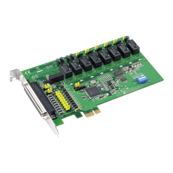
- Page 1 User Manual PCIE-1760 8-Ch Relay and 8-Ch Isolated Digital Input PCIE Card...
- Page 2 Because of Advantech’s high quality-control standards and rigorous testing, most of our customers never need to use our repair service. If an Advantech product is defec- tive, it will be repaired or replaced at no charge during the warranty period. For out- of-warranty repairs, you will be billed according to the cost of replacement materials, service time, and freight.
- Page 3 This product has passed the CE test for environmental specifications when shielded cables are used for external wiring. We recommend using shielded cables. This type of cable is available from Advantech. Please contact your local supplier for ordering information. FCC Class A This equipment has been tested and found to comply with the limits for a Class A dig- ital device, pursuant to Part 15 of the FCC rules.
- Page 4 PCIE-1760 User Manual...
-
Page 5: Table Of Contents
Figure 2.5 TTL type counter output signal connection....11 Figure 2.6 Sink type counter output signal connection ....12 2.1.4 Pin Assignment ................12 Figure 2.7 Pin assignment of PCIE-1760 ........12 2.1.5 Switch and Jumper Settings ............13 Chapter Function Details.........17... - Page 6 Figure 3.11Pulse width measurement ........21 Device Description and Configuration............. 21 Figure 3.12Device description shown in Navigator ....22 Appendix A Specifications........23 Isolation Digital Input................24 Relay Output ................... 24 Counter ....................25 General ....................26 Function Block Diagram................27 PCIE-1760 User Manual...
-
Page 7: Chapter 1 Introduction
Chapter Introduction... -
Page 8: Product Overview
Product Overview This chapter provides an overview of Advantech industrial data acquisition module for PCIE-1760 — surveying the product lineups, features, drivers, utilities, and acces- sories. PCIE-1760 are differential digital I/O modules. The function for these models are isolated digital I/O, TTL I/O, solid-state relay (SSR), and counters. -
Page 9: Driver Installation
PCIe system. All these soft- ware packages are available on the Advantech website: http://www.advantech.com/. The Advantech Navigator is a utility that allows you to set up, configure, and test your device; and later stores your settings in a proprietary database. -
Page 10: Software Development Using Daqnavi Sdk
Hardware Installation After the device driver installation has completed, you can now continue to install the PCIE-1760 card in any PCI Express slot on your computer. Follow the steps below to install the card on your system. Turn off your computer and unplug the power cord and cables. TURN OFF your computer before installing or removing any components on the computer. -
Page 11: Accessories
Remove button. Then go through the driver installation process again. After your card is properly installed on your system, you can now configure your device using the Advantech Navigator after you install XNavi on your computer. Accessories All of the following lists the accessories for PCIE-1760 PCL-10137-1E: 37-pin D-SUB cable, 1 m ... - Page 12 PCIE-1760 User Manual...
-
Page 13: Chapter 2 Installation And Field Applications
Chapter Installation and Field Applications... -
Page 14: Signal Connection And Pin Assignments
ON or OFF. In addition, do not input a voltage higher than the maximum allowable value of ON state or lower than the minimum allowable value of the OFF state, other- PCIE-1760 User Manual... -
Page 15: Relay Output Signal Connection
NO terminal, and the normally closed (NC) terminal is disconnected. On the other hand, if the relay is in OFF state, the COM terminal is connected to the NC terminal, and the NO terminal is disconnected. This is shown in Figure 2.3. The default state is OFF state. PCIE-1760 User Manual... - Page 16 However, both the load voltage and current must be within the range as specified in the device specifications for proper operation and to prevent the device from damage. Figure 2.4 Digital input signal connection with dry contact configuration PCIE-1760 User Manual...
-
Page 17: Counter Signal Connection
ON/OFF state of a switch. The state of the switch then decides if the load is conducting or not. The device supports sink (NPN) type configuration for counter output signal connection. This is shown in Figure 2.6. PCIE-1760 User Manual... -
Page 18: Pin Assignment
Figure 2.6 Sink type counter output signal connection 2.1.4 Pin Assignment Figure 2.7 Pin assignment of PCIE-1760 PCIE-1760 User Manual... -
Page 19: Switch And Jumper Settings
Relay output terminals. Can be configured 11 ~ 13, as normally close or normally open by on- 29 ~ 31 board jumpers. RLY<0..7>_COM Relay output common terminals. 14 ~ 19, 34, 37 2.1.5 Switch and Jumper Settings PCIE-1760 User Manual... - Page 20 Relay Output Configuration (JP8 – JP13) Jumper Setting Description Form A (normally open)* Form B (normally close) *Default setting Power-on Configuration (JP14) Jumper Setting Description Keep last status after hot reset Reset to default status after hot reset* *Default setting PCIE-1760 User Manual...
- Page 21 PWM Output Configuration (JP15 – JP16) Jumper Setting Description Sink (NPN)* 5V TTL * Default setting PCIE-1760 User Manual...
- Page 22 PCIE-1760 User Manual...
-
Page 23: Chapter 3 Function Details
Chapter Function Details... -
Page 24: Digital Input
Digital Input Insert an PCIE-1760 module supporting digital input function to perform digital input measurement. The following sections describe the digital input acquisition mecha- nism. For detailed specifications of the functions, refer to the document of the corre- sponding PCIE-1760 module. -
Page 25: Digital Input Debounce Filter
With instant digital input acquisition, the software controls the sample timing. Each time the software sends a “read instant digital input sample” command, the state of all digital input channels is sampled as shown in Figure 3.8. Figure 3.6 Instant digital input acquisition PCIE-1760 User Manual... -
Page 26: Digital Output
It can be configured rising edge or falling edge activating, as shown in Figure 3.28 and Figure 3.29, respectively. Figure 3.8 Rising edge event counting Figure 3.9 Falling edge event counting Counting may be temporarily paused by the counter gate signal as shown in Figure 3.30. PCIE-1760 User Manual... -
Page 27: Pulse Width Measurement
ID, model name and slot number. You can change the description in Navigator, or just leave it as default. The descrip- tion is used in your own program in order to get control or get a device handler from the device. PCIE-1760 User Manual... - Page 28 Figure 3.12 Device description shown in Navigator PCIE-1760 User Manual...
-
Page 29: Appendix A Specifications
Appendix Specifications... -
Page 30: Isolation Digital Input
30 V @ 2 A, 125 V @ 1 A: 3 x 10⁵ opera- Life expectancy tions min., 30 V @ 1 A, 125 V @ 0.5 A: Electrical operations min. Update type Static PCIE-1760 Series User Manual... -
Page 31: Counter
Counter output function External clock source 1 kHz max. frequency Delay count 1 ~ 4,294,967,295 One shot Gate source None, External (1 kHz max.) Gate polarity Rising edge or falling edge, software configurable Generation type Static PCIE-1760 Series User Manual... -
Page 32: General
37-pin D-sub Operating temperature 0 ~ 60 °C (32 ~ 140 °F) Storage temperature -20 ~ 70 °C (-4 ~ 158 °F) Operating humidity 10% to 90% RH, non-condensing Storage humidity 5% to 95% RH, non-condensing PCIE-1760 Series User Manual... -
Page 33: Function Block Diagram
Function Block Diagram PCIE-1760 Series User Manual... - Page 34 No part of this publication may be reproduced in any form or by any means, electronic, photocopying, recording or otherwise, without prior written permis- sion from the publisher. All brand and product names are trademarks or registered trademarks of their respective companies. © Advantech Co., Ltd. 2023...
Need help?
Do you have a question about the PCIE-1760 and is the answer not in the manual?
Questions and answers