Panasonic CQ-VW100U Service Manual
Dual din in-dash 7” widescreen color lcd monitor/dvd receiver
Hide thumbs
Also See for CQ-VW100U:
- Operating instructions manual (48 pages) ,
- Manual de instrucciones (46 pages)
Table of Contents
Advertisement
Quick Links
TABLE OF CONTENTS
1 Service Navigation ----------------------------------------------- 2
2 Specifications ----------------------------------------------------- 3
3 Features ------------------------------------------------------------- 4
4 Technical Descriptions ----------------------------------------- 5
5 Disassembly and Assembly Instructions ---------------11
6 Block Diagram----------------------------------------------------13
7 Wiring Connection Diagram ---------------------------------16
8 Schematic Diagram ---------------------------------------------17
9 Schematic Diagram-2 ------------------------------------------21
10 Printed Circuit Board-------------------------------------------23
11 Exploded View and Replacement Parts List -----------28
AUTOMOTIVE AFTERMARKET
Model No.
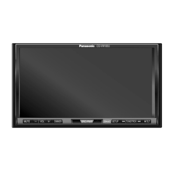
Dual DIN In-Dash 7" Widescreen Color
LCD Monitor/DVD Receiver
PAGE
© 2008 Matsushita Electric Industrial Co., Ltd. All
rights reserved. Unauthorized copying and distribu-
tion is a violation of law.
ORDER NO. ACED080107C1
CQ-VW100U
C7
PAGE
Advertisement
Table of Contents

Related Manuals for Panasonic CQ-VW100U


Summary of Contents for Panasonic CQ-VW100U
-
Page 1: Table Of Contents
ORDER NO. ACED080107C1 AUTOMOTIVE AFTERMARKET CQ-VW100U Model No. Dual DIN In-Dash 7” Widescreen Color LCD Monitor/DVD Receiver TABLE OF CONTENTS PAGE PAGE 1 Service Navigation ----------------------------------------------- 2 2 Specifications ----------------------------------------------------- 3 3 Features ------------------------------------------------------------- 4 4 Technical Descriptions ----------------------------------------- 5... -
Page 2: Service Navigation
1 Service Navigation 1.4. Maintenance Your product is designed and manufactured to ensure a mini- 1.1. About Lead Free Solder (PbF) mum of maintenance. Use a dry, a soft cloth for routine exterior cleaning. Never use benzine, thinner or other solvents. Distinction of PbF PCB : •... -
Page 3: Specifications
2 Specifications 2.2. Dimensions 2.1. Specifications* General Power Supply DC 12V (11V - 16V) Test Voltage 14.4V Negative Ground Current Consumption Less than 10A (during disc playback) Maximum Power Output 50 W x 4ch Power Output 20 W x 4ch 4 Ω... -
Page 4: Features
Panasonic DVD changer unit (CX-DH801U) - The optional adapter allows you to connect the optional Panasonic CD changer unit (CX-DP880) - TV Tuner (The optional Panasonic TV tuner unit: CY- TUN153U). - The optional adapter allows you to connect the optional iPod®... -
Page 5: Technical Descriptions
4 Technical Descriptions Port Description Vol (V) FM AM DV 4.1. Terminals Description D SCL DVD I2C clock output 3.3 3.3 3.3 BEEP Beep correspondence title 4.1.1. Main Block output REQUEST I2C communication request IC601:C2DBYY000345 (DVD DECK) Port Description Vol (V) D RESET DVD DECK`S reset output 3.3 3.3 3.3... - Page 6 Port Description Vol (V) Port Description Vol (V) FM AM DV FM AM DV BATT SENS Battery level detection 3.3 3.3 3.3 125 MONI CNT TFT monitor power supply 3.3 3.3 3.3 control output ACC SENS ACC level detection 5.2 5.2 5.2 126 Touch SW Switch output for touch PANEL DET Not connected...
- Page 7 4.2. IC Block Diagram 4.2.1. Main/Sub/Navi/ESC Block IC51 : C1BB00001045 IC202 : C1AB00002836 IC382 : C1AB00001870...
- Page 8 IC383 : C1AB00000163 IC201 : C1AA00000779 IC602 : C3FBHY000009 IC603 : C0JBAZ002217 IC251 : C1AB00000284 IC608 : C0JBAB000255...
- Page 9 IC705 : C0GBG0000032 IC701 : C0DAZHF00004 IC710 : C0CBCYG00004 IC702 : C0DBAZC00010 IC720 : C0DBEYY00005 4.2.2. TFT Block IC704 : C0EBY0000389 IC402 : AP2202KADJTR IC706 : C0DBCFG00011...
- Page 10 IC802 : C3EBCY000018 IC901 : C0ABBB000069 4.2.3. SW Block IC401 : C0DBAYY00269 IC451 : C0DBAYY00279 IC551 : PNA4S42M01MC IC452 : C0FBBY000047...
-
Page 11: Disassembly And Assembly Instructions
5 Disassembly and Assembly Instructions 5.1. How to Remove the Flexible PCB Disassembly of ESC Ass'y 1. Turn the unit upsidedown and draw out the ESC Ass'y. 3. Bend the ESC Ass'y forward and remove the FPC from CN452 of the TFT PCB. ESC Assy CN452 ESC Assy... - Page 12 5.2. How to Disassemble & assemble How to disassemble Remove the screw on the deck First take off the monitor block Lift the deck ass'y and remove the lock on the Sub shield. and must be as shown above. PCB CN252 Caution for breakage of the lock How to assemble Insert the flat cable of the deck to Sub PCB Match the deck ass'y with...
-
Page 13: Block Diagram
6 Block Diagram 6.1. Main-1/Sub-1 Block AUDIO PRE-OUT CN250 E-4C335a IC201 POWER AMP TU+B CN701 NAVI L TU+B R-CH IC202 CAR AUDIO PROCESSOR PA51 Q301 SW L FM/AM TUNER STBY LOUDNESS, MUTE Q302 VOLUME, MUTE ANT51 TONE MUTE (T,M,B) FADER L-CH R-CH IC701... - Page 14 6.2. Main-2/SW/TFT/LED Block E-4C336 E-4C335a IC801 DIGITAL VIDEO PROCESS CN901 XCLKI X801 CN151 CN452 27MHz (1/2) XCLKO (1/2) NAVI R ACR2 STHR W MODEL STH1 NAVI G ONLY STHL STH2 NAVI B ACB2 CPH1 AV VIDEO ACR0 CPH2 E-9943Aa IC906 CPH3 STVD W MODEL...
- Page 15 6.3. Main-3/Sub-2 Block E-4C335b(2/2) E-4C335a(3/3) CN259 W MODEL ONLY E-4C335c CN705 CN650 Q600 CN251 CN152 RM OUT 5 RM OUT IC382 (1/2) (1/2) NAVI SYNC 7 NAVI SYNC IC251 IC383 AV SWITCH Q611–613 VIDEO AMP Q351 NAVI R 9 RGB R NAVI L NAVI G 10 RGB G...
-
Page 16: Wiring Connection Diagram
7 Wiring Connection Diagram Video Input Terminal (AV1-IN) DVD Deck Video Input Terminal (AV2-IN) CN255 CN254 Flat Cable Jig Part No. CN605 YESFZS2071 SUB P.C.B [E-4C335b] CN259 CN711 CN252 CN251 LED P.C.B CN704 [E-4C335d] CAMERA IN CAMERA IN Yellow CN451 VIDEO OUT VIDEO OUT CN452... -
Page 17: Schematic Diagram
8 Schematic Diagram 8.1. Main Block E-4C335a IC701 PA51 J3CCBC000010 C0DAZHF00004 D717 B0ECKL000001 Q730,Q731 D701 D715 B1GBCFNN0009 Q701 B0BA04700003 B0JCPE000004 B1GBNCEJ0001 Q211,Q212,Q215,Q216 Q723,Q724 B1GDCFJJ0008 B1GDCFJJ0008 12.3 12.3 D704 B0ECKP000002 B1BBAC000014 Q201,Q202,Q301,Q302 J0LM00000001 B1GBCFGA0005 Q702,Q721,Q722 B1GBCFJN0009 D702 D712,D713 B0ECKP000002 B0ACCK000005 Q52,Q53 D722 D703,D721 B1GDCFJJ0008... - Page 18 8.2. Sub Block E-4C335b IC608 C0JBAB000255 The following symbols are shown on the schematic diagram. 3.3V 3.3V 2.5V 2.5V IC710 AUDIO (L,R) C0CBCYG00004 VISUAL Q351,Q352 B1ABCF000052 IC251 C1AB00000284 IC383 C1AB00000163 IC382 C1AB00001870 3.3V 3.3V 3.3V 3.3V 3.3V 3.3V 3.3V 3.3V 3.3V 3.3V 3.3V...
- Page 19 8.3. TFT Block E-4C336 3.3V 3.3V -10V -10V -10V D902 B0BD6R800002 D903 B0BD6R800002 IC901 Q901 C0ABBB000069 B1GBJCEJ0003 Q902 B1GBCFJN0009 3.3V 3.3V D803—D805 B0BC3R700004 3.3V 3.3V IC402 AP2202KADJTR 3.3V 1.8V 1.8V D401—D403 3.3V 3.3V B0JCGD000002 1.8V 1.8V 1.8V Q403—Q405 IC802 B1CHMC000009 C3EBCY000018 3.3V D913,D914...
- Page 20 8.4. SW Block...
-
Page 21: Schematic Diagram-2
9 Schematic Diagram-2 9.1. iPod Block... - Page 22 9.2. LED Block...
-
Page 23: Printed Circuit Board
10 Printed Circuit Board 10.1. Main/LED Block (Top View) - Page 24 10.2. Main/LED Block (Bottom View)
- Page 25 10.3. Sub Block...
- Page 26 10.4. TFT/SW Block (Top View)
- Page 27 10.5. TFT/SW Block (Bottom View)
-
Page 28: Exploded View And Replacement Parts List
11 Exploded View and Replacement Parts List 11.1. Exploded View (Unit) - Page 29 11.2. Replacement Parts List Notes : Ref. No. Part No. Part Name & Description Remarks Q302 B1GBCFGA0005 Transistor 1. Be sure to make your orders of replacement parts accord- Q351 B1ABCF000052 Transistor ing to this list. Q352 B1ABCF000052 Transistor 2. Important safety notice: Components, identified by Q600 B1GBCFJN0009 Transistor mark have special characteristics important for safety.
- Page 30 Ref. No. Part No. Part Name & Description Remarks Ref. No. Part No. Part Name & Description Remarks CAPACITORs C267 F2A1C470B260 Electrolytic 47MFD 16WV C290 F1J0J106A038 Ceramic 10MFD 6.3WV F1J1H470A732 Ceramic 47pF 50WV C291 F1J1C474A149 Ceramic 0.4MFD 16WV F1J1H103A733 Ceramic 0.01MFD 50WV C292 F1H1C473A071 Ceramic 0.047MFD 16WV...
- Page 31 Ref. No. Part No. Part Name & Description Remarks Ref. No. Part No. Part Name & Description Remarks C642 D0GBR00JA008 Chip 0W 1/10W D0GB222JA008 Chip 2.2k ohms 1/10W C643 D0GBR00JA008 Chip 0W 1/10W D0GB222JA008 Chip 2.2k ohms 1/10W C644 F1H1H221A841 Ceramic 220pF 50WV D0GB221JA008 Chip 220 ohms 1/10W...
- Page 32 Ref. No. Part No. Part Name & Description Remarks Ref. No. Part No. Part Name & Description Remarks R301 D0GB181JA008 Chip 180 ohms 1/10W R636 D0GA102JA012 Chip 1k ohms R302 D0GB181JA008 Chip 180 ohms 1/10W R637 D0GA102JA012 Chip 1k ohms R303 D0GB103JA008 Chip 10k ohms 1/10W...
- Page 33 Ref. No. Part No. Part Name & Description Remarks Ref. No. Part No. Part Name & Description Remarks R717 D0GD682JA017 Chip 6.8k ohms 1/8W RA612 D1H81024A043 Chip Network Resistor R718 D0GBR00JA008 Chip 0 ohms 1/10W RA613 D1H81024A043 Chip Network Resistor R719 D0GD471JA017 Chip 470 ohms 1/8W...
- Page 34 Ref. No. Part No. Part Name & Description Remarks Ref. No. Part No. Part Name & Description Remarks CN702 K1KA02AA0229 Connector 2pin C431 F1J1A106A023 Ceramic 10MFD 10WV CN703 K1KA02AA0229 Connector 2pin C435 F1H1H100A840 Ceramic 10pF 50WV CN704 YEAEJ220700A Connector-2pin C436 F1H1H100A840 Ceramic 10pF 50WV CN710...
- Page 35 Ref. No. Part No. Part Name & Description Remarks Ref. No. Part No. Part Name & Description Remarks C850 F1H1C104A107 Ceramic 0.1MFD 16WV R411 D0GB102JA008 Chip 1k ohms 1/10W C874 F1H1H103A842 Ceramic 0.01MFD 50WV R412 D0GB113JA008 Chip 11k ohms 1/10W C901 F1J1A106A023 Ceramic 10MFD 10WV...
- Page 36 Ref. No. Part No. Part Name & Description Remarks Ref. No. Part No. Part Name & Description Remarks R954 D0GB102JA008 Chip 1k ohms 1/10W CN902 K1MN08BA0189 Connector 8pin R955 D0GB221JA008 Chip 220 ohms 1/10W CN903 K1MN12BA0189 Connector 12pin R956 D0GB221JA008 Chip 220 ohms 1/10W R957 D0GB330JA008...
- Page 37 Ref. No. Part No. Part Name & Description Remarks Ref. No. Part No. Part Name & Description Remarks CONNECTOR YEFAASB7F35 DC Fan YFX214C398ZA RCA Bracket (UP) CN551 K1MY12BA0173 Connector 12pin YFR044C013ZA RCA Cap YFX214C486CA Bracket, Sub PCB Accessories YFX214C357ZB Bracket, IC701 YFX214C403CA Bracket, IC201 PRINTINGs YFX214C466ZA...
- Page 38 11.3. Packing Parts List Unit • Item numbers listed below should not order regular spare parts. (not available) Item No. Parts No. Part Name & Description Q'ty Remarks Inner Carton Not available Packing Pad (Left) Not available Packing Pad (Right) Not available Packing Pad (A) Not available...
-
Page 39: Schematic Diagram For Printing With Letter Size
12 Schematic Diagram for Printing with Letter Size 12.1. Main Block (Left Side) IC701 C0DAZHF00004 D717 B0ECKL000001 D715 D701 Q701 B0JCPE000004 B0BA04700003 B1GBNCEJ0001 Q211,Q212,Q215,Q216 Q723,Q724 B1GDCFJJ0008 B1GDCFJJ0008 12.3 12.3 D704 B0ECKP000002 Q201,Q20 B1GBC Q702,Q721,Q722 B1GBCFJN0009 D712,D713 D702 B0ECKP000002 B0ACCK000005 D722 D703,D721 B0ECKP000002 B0ACCK000005... - Page 40 12.2. Main Block (Right Side) E-4C335a PA51 J3CCBC000010 Q730,Q731 B1GBCFNN0009 B1BBAC000014 Q201,Q202,Q301,Q302 J0LM00000001 B1GBCFGA0005 Q52,Q53 B1GDCFJJ0008 The following symbols are shown on the schematic diagram. B0ACCK000005 IC202 C1AB00002836 B1CBGF000005 IC51 C1BB00001045 3.3V 3.3V 2.5V 2.5V RADIO (L,R) AUDIO (L,R) VISUAL NAVI(R,G,B) 3.3V Q158...
- Page 41 12.3. Sub Block (Left Side) E-4C335b IC608 C0JBAB000255 IC710 C0CBCYG00004 IC382 C1AB00001870 3.3V 3.3V 3.3V 3.3V 3.3V 3.3V 3.3V 3.3V 3.3V...
- Page 42 12.4. Sub Block (Right Side) E-4C335b The following symbols are shown on the schematic diagram. 3.3V 3.3V 2.5V 2.5V AUDIO (L,R) VISUAL Q351,Q352 B1ABCF000052 IC251 C1AB00000284 IC383 C1AB00000163 IC382 C1AB00001870 3.3V 3.3V 2.5V 2.5V IC706 C0DBCFG00011 CQ-VW100W/N/U SUB...
- Page 43 12.5. TFT Block (Left Side) 3.3V 3.3V -10V Q901 B1GBJCEJ0003 Q902 B1GBCFJN0009 3.3V 3.3V IC402 AP2202KADJTR 1.8V 1.8V D401ÐD403 B0JCGD000002 Q403ÐQ405 B1CHMC000009 3.3V -10V The following symbols are shown on the schematic diagram. Q401 B1GBNCEJ0001 3.3V IC401 3.3V C0DBAYY00269 1.8V 1.8V -10V -10V...
- Page 44 12.6. TFT Block (Right Side) E-4C336 -10V -10V -10V D902 B0BD6R800002 D903 B0BD6R800002 IC901 C0ABBB000069 3.3V D803ÐD805 B0BC3R700004 3.3V 3.3V 3.3V 3.3V 1.8V 1.8V 1.8V IC802 C3EBCY000018 D913,D914 B0BC5R600010 IC801 C0HBA0000245 3.3V IC906 C0BBAA000039 D915 B0BC5R600010 1.8V 1.8V 3.3V 0.22u 1.8V 1.8V 3.3V...
- Page 45 12.7. SW Block (Left Side)
- Page 46 12.8. SW Block (Right Side)
- Page 47 Printed in Taiwan 2008.03...
Need help?
Do you have a question about the CQ-VW100U and is the answer not in the manual?
Questions and answers