Table of Contents

Related Manuals for FRIENDCOM FC-301D


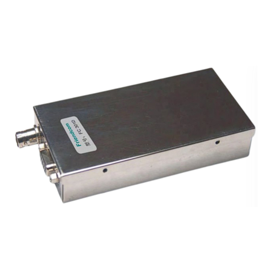
Summary of Contents for FRIENDCOM FC-301D
- Page 1 FC-301D SERVICE MANUAL SHENZHEN FRIENDCOM TECHNOLOGY DEVELOPMENT CO.,LTD ADD: 2/F MULTIFUNCTION BUILDING DONGPENG INDUSTRIAL PARK WUHAO ROAD NORTH SECTION OF HI-TECH PARK SHENZHEN 518057 CHINA TEL: +86-755-86026600 FAX: +86-755-86026300...
-
Page 2: Table Of Contents
MAINTENANCE AND REPAIR........18 PROGAMMING..........21 ALIGNMENT PROCEDURE........37 ALIGNMENT POINTS DIAGRAM......43 COMPONENT REPLACEMENT........44 TROUBLESHOOTING GUIDE.........48 WIRING DIAGRAM..........49 FC-301D DIGITAL BOARD PARTS LIST ......50 DIGITAL BOARD SCHEMATIC ........54 DIGITAL PCB ASSEMBLY ........58 FACTORY SETTING DIAGRAM .......60 EXPLODED VIEW & PARTS LIST ......61 - 1 -... -
Page 3: Specifications
SPECIFICATION GENERAL ………………………………… Equipment Type Data Radio Performance Specification…………....TIA/EIA-603 & ETS 300-113 Band …………………………………………... UHF/VHF Channel Spacings……………………………… 25KHz,12.5KHz programmable RF Output Power………………………………. 1W / 5W Programmable Modulation type ……………………………….. 16K0F3E,8K5F3E Intermediate Frequency………………………… 45.1MHz & 455KHz Number of Channels……………………………. Frequency Source ………………………………. Synthesizer Operation Rating…………………………………... - Page 4 Frequency Bands : ……………………………… UHF: U1 400 – 470 MHz …………………..……………. UHF: U1 400 – 470 MHz Dimensions……………………………………….. (120mm)L x (60mm)W x (20mm)H Weight…………………………………………….. ≤150 grams TRANSMITTER Sustained Transmission…………………………… Nominal conditions Time: 30 sec Power: >95% >95% >90% ±2.5 ppm Frequency Error…………………………………..
- Page 5 12.5kHz Channel Spacing………………..…… >36 dB (with POSPH) Modulation Symmetry ……………………………. .<10% Peak Dev@1kHz input for nominal dev +20dB Load Stability…………………………………… No osc at >= 10:1 VSWR all phase angles and suitable antenna No destroy at >= 20:1 all phase angle RECEIVER Sensitivity(12dB Sinad) …………………………..
- Page 6 12.5kHz CP ………………………………………..…< 40dB with PSOPH Receiver Response Time …………………………….< 20ms Squelch Opening sensitivity: ………………………-118dBm ……………………….. -121dBm Squelch Closing sensitivity Squelch Attack Time: RF Level at Threshold ………………………… <40ms RF Level at Threshold +20dB …………………<30ms L.O. Frequency Temperature Stability …………….1 st <2.5 ppm, 2 nd <10 ppm for –30°C to +60°C L.O.
- Page 7 Recharging ……………………………………………… -10 to +55 ………………………………………………………. 20kV (C-MIC >= 15kV) Vibration ………………………………………………… MIL STD 810 C Procedures I,II,V and IEC68 26 · Due to contintuning researching and development the company reserves the right to alter these specifications without prior notice. - 6 -...
-
Page 8: Fc-301D Circuit Diagram
FC-301D CIRCUIT DIAGRAM - 7 -... -
Page 9: Introduction
INTORDUCTION The FC-301D Series of RF Link Modules from Friendcom utilizes the latest technology in its design and manufacturing. Both the UHF and VHF models are PLL (Phase Lock Loop Synthesizer) / microprocessor controlled, and offer one to five watts of power with 16 channel capability. Multiple functions... -
Page 10: Theory Of Operation
THEORY OF OPERATION The Base Band signal circuits It contains the CPU, power circuit ,TX signal circuit,RX signal circuit. The CPU circuit and power circuit From Block Digram above: The DC power was regulated to 8 volt by IC500 ,and supplied to the RF part. IC504 convert 8 volt to 5volt and supply to IC510. - Page 11 The CPU SQ pin detect the signal from PIN14 of IC2. when there is no receiveing signal, the input level is about 1.2V, and PIN8 of IC510 output high level(5V). When detect input receiving signal, the input level is about 0V, and PIN8 of IC510 output low level(5V).
- Page 12 through MIC-IN port and amplified by U1B; then it will divide into two signal, one will coupling by C405 R407 and fed to TCXO for TX modulation; the other one was amplified by U1C,after coupling by C428,R404,C427 ;the voice signal is filtered by U1D which is a low pass filter, the output of U1D is then fed to VCO for TX modulation after coupling by C415,R403 again.
- Page 13 RF circuit Main include PLL circuit / TX circuit /RX circuit PLL Frequency Synthesizer From the above Block Diagram : PLL circuit generates the first local oscillator signal for reception and RF signal for transmission. 1. PLL Circuit Step frequency of PLL can be 5.0 KHz or 6.25 KHz. A 13MHz reference oscillator signal is divided at IC301 by a counter to generate a 5.0 KHz or 6.25 KHz reference frequency.
- Page 14 to generate a level D.C., and the level D.C. controls oscillator frequency by controlling VCO. 2. VCO The operating frequency is generated by Q302 in transmit mode and by Q307 in receive mode. Operating frequency generate a control voltage by phase comparator to control varactor diodes so that the oscillator frequency is consistent with the MCU preset frequency(D301、D302、D303 and D304 in transmit mode, and D307、...
- Page 15 Receiver The receiver utilizes double conversion superheterodyne (UHF)/(VHF). 1. Front-end RF Amplifier The signal from antenna is amplified at LNA (Q15) after passing through a transmit/receive circuit band pass filter (D211/D212/D241/C264/C260/L25/L26). Before passing the first mixer (T3、T4、TC3), the amplified signal is filtered through another band pass filter(D208/D209/C240/C257/C258/L23/L24)...
- Page 16 2. First Mixer The signal from RF amplifier is mixed with the first local from PLL frequency synthesizer circuit at the fix mixer (T3、T4、TC3) to create a 45.1MHz first IF signal. The first IF signal is then amplified by Q13 and fed through a crystal filter (XF1) to further remove unwanted signals.
- Page 17 Transmitter 1. RF Power Amplifier The transmit signal from VCO buffer amplifier (Q304、Q111) is amplified by Q1 and Q2. The amplified signal is then amplified by the power amplifier I102 to create 5.0W RF power. Antenna Switch and LPF Output signal from RF amplifier passes through a low-pass filter network and a transmit/receive switch circuit comprised of D102,D106 and D107 before it reaches the antenna terminal.
- Page 18 3. APC The automatic power control (APC) circuit stabilizes the transmit output power by detecting the forward and backward power of final stage amplifier. IC1 (2/2) compares the preset reference voltage with the voltage obtained from the regulated power signal. APC voltage is proportional to the forward and backward power.
-
Page 19: Maintenance And Repair
When removing or fitting, use the Exploded View and Parts List, located on page in conjunction with the following procedures: · WARNING: Disconnect the FC-301D from all external equipment at the connector prior to disassembly. REMOVING & REPLACING THE UPPER COVER Removing the Upper Cover: 1. - Page 20 REMOVING&REPLACING THE INTERPHASE CONNECTION BOARD Removing the interphase connection board: 1.Remove the Upper Cover (refer to Removing & Replacing the Upper Cover). 2.Disconnect the DB9 pin connector on CON401. 3.Unscrew the two mounting screws on the Amplifier module. 4.Remove the interphase connection board directly. To replace interphase connection board: 1.
- Page 21 REMOVING & REPLACING THE RF BOARD Removing the RF Board Assembly: 1.Remove the Upper Cover (refer to Removing & Replacing the Upper Cover). 2.Remove the interphase connection board (refer to Removing & Replacing the interphase connection board). 3. Unscrew the 4 mounting screws 4.
-
Page 22: Progamming
Ⅰ. To start the FC-301/D Program Software and read the parameters of FC-301/D RF Link Module Firstly make sure to connect data port J1 of FC-301D with PC via RS232 data cable. Double click the "FC301D.exe". The software will enter into main... - Page 23 Run the ‘Port’ in the main menu or press the Icon ‘Port ’ , The software will enter into the Port parameter setting interface. - 22 -...
- Page 24 Run ‘ Program ’ -> ‘ Read ’ in the main menu, The software will detect and read the parameters of FC-301D. - 23 -...
- Page 25 After run step 4, FC-301/D will automatically detect the FC-301/D RF link module and display the parameters of the module on the screen. - 24 -...
- Page 26 Ⅱ. To change the parameters of the RF link module After reading the previous parameters, User can change the parameters of the module to new ones. Model:Only for check, it can not be changed. Serial No:Input 5 digits for ID code. Zero will be added to the front. The value less than 65536.
- Page 27 Ⅲ. To write the parameters into the module Run ‘Program’ -> ‘ Write ’ in the main menu, The changed parameters will be written into the FC-301/D module. - 26 -...
- Page 28 Ⅳ. To read / write the frequency Click the button ‘Read Frequency’, the frequency of the channel from 1-16 will be displayed on the screen. - 27 -...
- Page 29 - 28 -...
- Page 30 New frequency can be input into each channel and click the ‘Write Frequency’ button, the new frequency will be written into the module. - 29 -...
- Page 31 - 30 -...
- Page 32 Ⅴ. The switch between 12.5kHz and 25kHz channel spacing In the ‘Band Control ’ interface, Click ‘Read’ , the current channel spacing 12.5kHz or 25kHz can be read out. Click ‘Set’, the selected channel spacing 12.5kHz or 25kHz can be written into the module. - 31 -...
- Page 33 Ⅵ. To adjust the parameters While the module works in transmission or reception status on one fixed frequency, Click ‘Set’ in ‘Adjust Parameter’ to adjust the sensitivity or the RF power on one frequency. Click ‘Read’ to read the adjusted parameters of the current frequency.
- Page 34 econdly input the corresponding value in ‘Adjust Parameter’ according to channel frequency ;you will see ‘Setting successful’after you click ‘set’. Otherwise you will see ‘Setting no answer’which indicate setting fail. Thirdly,after setting success you can wait for 10 seconds or switch channel button to make the newest parameter be stored in CPU.
- Page 35 Read the Turning Value of RX (TV Value) Fristly adjust CON1 pin8 SW port to low level and change RF at the status of RX ; Secondly click the button ‘Read’ in Adjust Parameter,you will see ‘Reading success’message and the detail parameter below; otherwise you will see ‘Reading no answer’and it indicate read failed it need to read again .(Without necessary please remmeber not to change the turning value which have set in...
- Page 36 ‘Reading success’message and the detail parameter below; otherwise you will see ‘Reading no answer’and it indicate read failed and need to read again . Ⅶ. To save or open parameter file Run ‘File’->‘Save’ menu, The ‘Save’ interface will be displayed on the screen, Input the file name for saving, and press ‘Save’...
- Page 37 Run ‘File’->‘Open’ menu, The ‘open’ interface will be displayed on the screen, Choose the file name which saved the parameters, and press ‘Open’ button, the parameters of the module saved in the file will be displayed on the screen. - 36 -...
-
Page 38: Alignment Procedure
ALIGNMENT PROCEDURE The FC-301D is by design, broad band covering UHF(400-470 MHz) and should require no special alignment, unless repairs are performed on the receiver portion. Should repairs be necessary, use the "Alignment Points Diagram" on page, in conjunction with the following procedures: PCB Testing 1.Adjust the power supply voltage to 12.5V before connect FC-301D to... - Page 39 1.Set Wireless Conmmunication Test set at the status of RX Test 2. Set the audio out of Wireless Conmmunication Test set as 1K; the amplitude of sinusoidal signal as 100mV. 3.Connect the audio output to CONI pin1 of FC301D,switch S1 to MIC-IN;then adjust the RF at the status of TX , connect the audio output to TP4 ,adjust VR403 for a reading of audio signal amplitude as 58mV and distortion is less than 3%...
- Page 40 frequency of Wireless Conmmunication Test set as 1KHz; the amplitude of sinusoidal signal as 100mV.Secondly test channe 1 ,8 and 16 separately for a reading of TX power 20mV+5mW, frequency deviation 3KHZ+0.5KHz and distortion is less than 3%; Also off the output signal of Test Set the frequency deviation should less than 70Hz.
- Page 41 3%; Also off the output signal of Test Set the frequency deviation should less than 80Hz. RX Wide Band Test of FC-301D 1.Set Wireless Conmmunication Test Set at the status of TX Test , and the...
- Page 42 modulation signal of Test set have to be setted field intensity as 1mv ,frequency as 1KHz and frequency deviation as 3kHz. Also set FC301D at the status of RX 2.Please refer to wiring diagram and operation on page to testing for a reading of AF OUT level to be 210+20mV and ditortion less than 5% 3.Please refer to Turning Value on page ? ,set the RF output signal of the Test Set to 0.28μV and test the Sinad,it should be better than 12dB.
- Page 43 4.When Sinad drop to be 10dB, SQ should be high level output and Voltage range should be more than 4.5V; When Sinad rise to more than 12dB, SQ should be low level output and Voltage range should be less than 0.4V; 5.Testing the RSSI output level should to be 2.2V-0.8V 6.
-
Page 44: Alignment Points Diagram
ALIGNMENT POINTS DIAGRAM DIGITAL BOARD ALIGNMENT POINTS CHANNEL SELECT SWITCH - 43 -... -
Page 45: Component Replacement
COMPONENT REPLACEMENT Surface Mount Components Surface mount components should always be replaced using a temperature controlled soldering system. The soldering tools may be either a temperature controlled soldering iron or a temperature controlled hot-air soldering station. A hot-air system is recommended for the removal of components on these boards. - Page 46 cord connected to an outlet with a known good earth ground. When soldering or desoldering a CMOS device, the soldering equipment should have a known good earth ground. Surface Mount Removal 1.Grip the component with tweezers or small needle nose pliers. 2.Alternately heat the metalized terminal ends of the surface mount component with the soldering iron.
- Page 47 2.Place the component on the PCB pads, observing proper polarity for capacitors, diodes, transistors, etc. 3.Simultaneously touch the “tinned” terminal end and the “tinned” pad with the soldering iron. Slightly press the component down on the board as the solder liquefies. Solder all terminals, allowing the component time to cool between each application of heat.
- Page 48 The hot-air soldering system is the best method of replacing surface mount ICís. The IC’s can easily be removed and installed using the hot-air system. See the manufacturerís instructions for complete details on tip selection and other operating instructions unique to your system. If a hot-air system is not available, the service technician may wish to clip the pins near the body of the defective IC and remove it.
-
Page 49: Troubleshooting Guide
TROUBLESHOOTING GUIDE SYMPTOM S CAUSES COUNTERMEASURES 1.No power incomplete connection 1.Check COM1 connection 2. No input voltage of 5V or 8V 2. Check IC500、IC504 Unit does not work 3. CPU does not work 3. Check IC510 4. EEPROM fail 4. Check IC502 5. -
Page 50: Wiring Diagram
WIRING DIAGRAM - 49 -... -
Page 51: Fc-301D Digital Board Parts List
FC-301D DIGITAL BOARD PARTS LIST - 50 -... - Page 52 - 51 -...
- Page 53 - 52 -...
- Page 54 - 53 -...
-
Page 55: Digital Board Schematic
- 54 -... - Page 56 - 55 -...
- Page 57 - 56 -...
- Page 58 - 57 -...
-
Page 59: Digital Pcb Assembly
- 58 -... - Page 60 - 59 -...
-
Page 61: Factory Setting Diagram
FACTORY SETTING DIAGRAM Channel RX Frequency RX Turning TX Turning Value (TV) Frequency Value (APC) 400.1250MHZ 400.1250MHZ 405.1250MHZ 405.1250MHZ 410.1250MHZ 410.1250MHZ 415.1250MHZ 415.1250MHZ 420.1250MHZ 420.1250MHZ 425.1250MHZ 425.1250MHZ 430.1250MHZ 430.1250MHZ 435.1250MHZ 435.1250MHZ 436.1250MHZ 436.1250MHZ 440.1250MHZ 440.1250MHZ 445.1250MHZ 445.1250MHZ 450.125MHZ 450.1250MHZ 455.1250MHZ 455.1250MHZ 460.1250MHZ 460.1250MHZ... -
Page 62: Exploded View & Parts List
EXPLODED VIEW & PARTS LIST ITEM # NAME QUANTITY DESCRIPTION Label self-adhesive paper Front crust stainless steel Interphase connection board Standard component Plug-In unit Standard component PCB board Standard component Shielding case Tinplate (nickel plating) Shielding case B Tinplate (nickel plating) Shielding case C Tinplate(nickel plating) Cold sink... - Page 63 - 62 -...
Need help?
Do you have a question about the FC-301D and is the answer not in the manual?
Questions and answers