Table of Contents
Advertisement
Quick Links
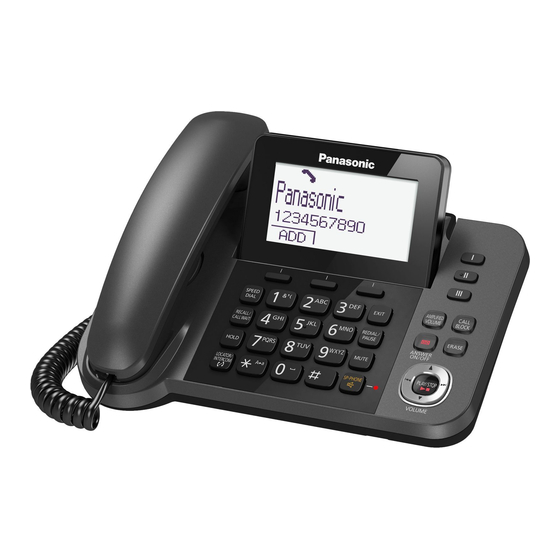
KX-TGFA30
(Handset)
(Charger Unit)
Configuration for each model
Model No
Base Unit
KX-TGF380 1 (TGF380) 1 (TGFA30)
KX-TGF380
(Base Unit)
Handset
Charger Unit
1
Telephone Equipment
KX-TGF380AGM
Model No.
KX-TGFA30AGM
Digital Corded/Cordless Phone with
Link-to-Cell
M: Metallic Black Version
(for Argentina)
© Panasonic System Networks Co., Ltd. 2015
Unauthorized copying and distribution is a violation
of law.
ORDER NO. KM41511964CE
Advertisement
Table of Contents

Related Manuals for Sony KX-TGF380AGM


Summary of Contents for Sony KX-TGF380AGM
- Page 1 ORDER NO. KM41511964CE Telephone Equipment KX-TGF380AGM Model No. KX-TGFA30AGM Digital Corded/Cordless Phone with Link-to-Cell M: Metallic Black Version (for Argentina) KX-TGFA30 KX-TGF380 (Handset) (Base Unit) (Charger Unit) Configuration for each model Model No Base Unit Handset Charger Unit KX-TGF380 1 (TGF380) 1 (TGFA30) ©...
- Page 2 KX-TGF380AGM/KX-TGFA30AGM WARNING This service information is designed for experienced repair technicians only and is not designed for use by the general public. It does not contain warnings or cautions to advise non-technical individuals of potential dangers in attempting to service a product. Products powered by electricity should be serviced or repaired only by experienced professional technicians.
-
Page 3: Table Of Contents
KX-TGF380AGM/KX-TGFA30AGM TABLE OF CONTENTS PAGE PAGE 1 Safety Precautions----------------------------------------------- 5 10.1.10. Check Handset Reception ------------------------ 44 1.1. For Service Technicians --------------------------------- 5 10.1.11. Check Caller ID ------------------------------------- 44 2 Warning -------------------------------------------------------------- 5 10.1.12. Check BT Communication ------------------------ 45 2.1. Battery Caution--------------------------------------------- 5 11 Disassembly and Assembly Instructions--------------- 47 2.2. - Page 4 16.2. Cabinet and Electrical Parts (Handset) ------------- 99 16.3. Cabinet and Electrical Parts (Charger Unit) ----- 100 16.4. Accessories and Packing Materials --------------- 101 16.4.1. KX-TGF380AGM ---------------------------------- 101 16.5. Replacement Parts List ------------------------------- 102 16.5.1. Base Unit -------------------------------------------- 102 16.5.2. Handset ---------------------------------------------- 104 16.5.3.
-
Page 5: Safety Precautions
KX-TGF380AGM/KX-TGFA30AGM 1 Safety Precautions 1.1. For Service Technicians • Repair service shall be provided in accordance with repair technology information such as service manual so as to prevent fires, injury or electric shock, which can be caused by improper repair work. -
Page 6: Suggested Pbf Solder
KX-TGF380AGM/KX-TGFA30AGM 2.2.1. Suggested PbF Solder There are several types of PbF solder available commercially. While this product is manufactured using Tin, Silver, and Copper (Sn+Ag+Cu), you can also use Tin and Copper (Sn+Cu), or Tin, Zinc, and Bismuth (Sn+Zn+Bi). Please check the manufacturer's specific instructions for the melting points of their products and any precautions for using their product with other materials. -
Page 7: Specifications
KX-TGF380AGM/KX-TGFA30AGM 3 Specifications L Standard: DECT 6.0 (Digital Enhanced Cordless Telecommunications 6.0), Bluetooth wireless technology 2.1 L Frequency range: 1.91 GHz to 1.93 GHz (DECT) 2.402 GHz to 2.48 GHz (Bluetooth) L RF transmission power: 115 mW (max) L Power source:... -
Page 8: Technical Descriptions
KX-TGF380AGM/KX-TGFA30AGM 4 Technical Descriptions 4.1. Circuit Configuration of TGF38x Series Phones TGF38x Series consists of DECT cordless telephone and Bluetooth Module. Both voices of transmission and reception are transferred by PCM. BBIC on DECT side controls the cordless telephone system, which makes control data communication with BT_IC on BT Module in serial data. -
Page 9: Dect Description
KX-TGF380AGM/KX-TGFA30AGM 4.2. US-DECT Description Transmitting and receiving carrier between base unit and handset is same frequency. 4.2.1. TDD Frame Format 5 ms 5 ms Up Link ( Handset - > Base Unit ) Down Link ( Base Unit - > Handset ) DATA rate : 1.152 Mbps... -
Page 10: Signal Flowchart In The Radio Parts
KX-TGF380AGM/KX-TGFA30AGM 4.2.3. Signal Flowchart in the Radio Parts Reception Base unit: A voice signal from TEL line is encoded to digital data and converted into a 1.9GHz modulated radio signal by BBIC(IC501). The RF signal, after which is amplified in BBIC, is fed to selected antenna. -
Page 11: Block Diagram (Base Unit_Main)
KX-TGF380AGM/KX-TGFA30AGM 4.3. Block Diagram (Base Unit_Main) RF_VDD VDD_PA... -
Page 12: Tel Interface Circuit
KX-TGF380AGM/KX-TGFA30AGM 4.4. Tel Interface Circuit R141... -
Page 13: Block Diagram (Base Unit_Rf Part)
KX-TGF380AGM/KX-TGFA30AGM 4.5. Block Diagram (Base Unit_RF Part) -
Page 14: Circuit Operation (Base Unit)
KX-TGF380AGM/KX-TGFA30AGM 4.6. Circuit Operation (Base Unit) General Description: (BBIC, Flash Memory, EERROM) is a digital speech/signal processing system that implements all the functions of speech compression, record and playback, and memory management required in a digital telephone answering machine. The BBIC system is fully controlled by a host processor. The host processor provides activation and control of all that functions as follows. -
Page 15: Power Supply Circuit/Reset Circuit
KX-TGF380AGM/KX-TGFA30AGM 4.6.5. Power Supply Circuit/Reset Circuit There are 2 pattern from power supply voltage. 1) AC adapter voltage is converted to VBAT(3.0V) at DCDC converter. 2) Battery voltage goes through to VBAT(Battery voltage). VBAT is used for various voltage of the system. -
Page 16: Telephone Line Interface
KX-TGF380AGM/KX-TGFA30AGM 4.6.6. Telephone Line Interface Telephone Line Interface Circuit: Function • Bell signal detection • ON/OFF hook and pulse dial circuit • Side tone circuit Bell (RINGING) signal detection and OFF HOOK circuit: In the idle mode, Q141 is open to cut the DC loop current and decrease the ring load. When ring voltage appears at the Tip (T) and Ring (R) leads (When the telephone rings), the AC ring voltage is transferred as follows: L1T ... -
Page 17: Parallel Connection Detect Circuit/Auto Disconnect Circuit
KX-TGF380AGM/KX-TGFA30AGM 4.6.7. Parallel Connection Detect Circuit/Auto Disconnect Circuit Function: In order to disable call waiting and stutter tone functions when using telephones connected in parallel, it is necessary to have a circuit that judges whether a telephone connected in parallel is in use or not. This circuit determines whether the telephone connected in parallel is on hook or off hook by detecting changes in the T/R voltage. -
Page 18: Calling Line Identification (Caller Id)/Call Waiting Caller
KX-TGF380AGM/KX-TGFA30AGM 4.6.8. Calling Line Identification (Caller ID)/Call Waiting Caller ID Function: Caller ID The caller ID is a chargeable ID which the user of a telephone circuit obtains by entering a contract with the telephone company to utilize a caller ID service. For this reason, the operation of this circuit assumes that a caller ID service contract has been entered for the circuit being used. - Page 19 KX-TGF380AGM/KX-TGFA30AGM Call Waiting Caller ID Calling Identity Delivery on Call Waiting (CIDCW) is a CLASS service that allows a customer, while off-hook on an existing call, to receive information about a calling party on a waited call. The transmission of the calling information takes place almost immediately after the customer is alerted to the new call so he/she can use this information to decide whether to take the new call.
-
Page 20: Block Diagram (Handset)
KX-TGF380AGM/KX-TGFA30AGM 4.7. Block Diagram (Handset) ANT1 EEPROM 13.824 MHz VBAT CHG_DET CHARGE RSTN RESET RF part CONTROL CHARGE CHG_CTL POWER SUPPLY CONTROL BATTERY_ON VBAT BATTERY BBIC Receiver HSSPOUTP Headset Jack LOUT HSMIP 4.0V VBAT CHARGE HEADSET_DET (KEY) CP_OFF PUMP KEY_LED... -
Page 21: Block Diagram (Handset_Rf Part)
KX-TGF380AGM/KX-TGFA30AGM 4.8. Block Diagram (Handset_RF Part) KX-TGFA30 BLOCK DIAGRAM (Handset_RF Part) -
Page 22: Circuit Operation (Handset)
KX-TGF380AGM/KX-TGFA30AGM 4.9. Circuit Operation (Handset) 4.9.1. Outline Handset consists of the following ICs as shown in Block Diagram (Handset) (P.20). • DECT BBIC (Base Band IC): IC1 - All data signals (forming/analyzing ACK or CMD signal) - All interfaces (ex: Key, Detector Circuit, Charge, EEPROM, LCD) •... -
Page 23: Charge Circuit
KX-TGF380AGM/KX-TGFA30AGM 4.9.3. Charge Circuit Circuit Operation: Charge +(charger) CHARGE +(Handset) R8 Q3 F1 BATTERY(+) BATTERY(-) R45 GND CHARGE -(Handset) Charge -(charger) In this way, the BBIC on Handset detects the fact that the battery is charged. -
Page 24: Circuit Operation (Charger Unit)
KX-TGF380AGM/KX-TGFA30AGM 4.10. Circuit Operation (Charger Unit) Charge control is executed at handset side so that the operation when using charger is also controlled by handset. Refer to Circuit Operation (Handset) (P.22) AC Adaptor The route for this is as follows: DC+pin of J1(+) CHARGE+pad Handset CHARGE-pad DC-pin of J1(-). -
Page 25: Location Of Controls And Components
KX-TGF380AGM/KX-TGFA30AGM 5 Location of Controls and Components Refer to the Operating Instructions. Note: You can download and refer to the Operating Instructions (Instruction book) on TSN Server. 6 Installation Instructions Refer to the Operating Instructions. Note: You can download and refer to the Operating Instructions (Instruction book) on TSN Server. -
Page 26: Test Mode
KX-TGF380AGM/KX-TGFA30AGM 8 Test Mode 8.1. Engineering Mode 8.1.1. Base Unit Important: Make sure the address on LCD is correct when entering new data. Otherwise, you may ruin the unit. {OFF} (Off) Soft keys Navigator key/ VOL.(Volume) key Dial keypad This pictured model is for KX-TGF380. - Page 27 KX-TGF380AGM/KX-TGFA30AGM Set Addr.: 7). Press , a long confirmation beep New Data will be heard. CLEAR 8). Press {OFF} to return to standby mode. Set Addr.: After that, turn the base unit power off and then power on. _ _ _ _ BACK Note: * To enter "Set dial mode", press {...
-
Page 28: Handset
KX-TGF380AGM/KX-TGFA30AGM 8.1.2. Handset Important: Make sure the address on LCD is correct when entering new data. Otherwise, you may ruin the unit. {OFF} (Off) Soft keys Navigator key/ VOL.(Volume) key Dial keypad {FLASH} {CALL WAIT} (Call wait) H/S key operation H/S LCD 1). - Page 29 KX-TGF380AGM/KX-TGFA30AGM Frequently Used Items (Handset) ex.) Items Address Default Data New Data Possible Adjusted Possible Adjusted Remarks Value MAX (hex) Value MIN (hex) Battery Low 00 09 (*2) Frequency 00 07 / 00 08 00 / 01 00 02 ~ 00 06...
-
Page 30: Service Mode
KX-TGF380AGM/KX-TGFA30AGM 9 Service Mode 9.1. How to Clear User Setting (Handset Only) Handset Press simultaneously until a beep sound is heard. Then single handset is initialized. (The contents of user setting are reset to factory default) *Usage time is not cleared. -
Page 31: Troubleshooting Guide
KX-TGF380AGM/KX-TGFA30AGM 10 Troubleshooting Guide 10.1. Troubleshooting Flowchart FLOW CHART Not working Power ON Base Unit Check Power Not recording (*1) Record Check Record No playback Playback Pre-Message Check Playback Link No link Not charged Battery Charge Check Battery Charge Check Link... -
Page 32: Check Power
KX-TGF380AGM/KX-TGFA30AGM 10.1.1. Check Power 10.1.1.1. Base Unit Is the AC Adaptor inserted into AC outlet? (*1) AC Adaptor. Is output voltage of AC adaptor 5.5 V? Check Check Power Supply Circuit. Check VDD1(1.8V) :Test point (VDD1) RSTN: Reset = "High"? Check Reset Circuit. -
Page 33: Check Record
KX-TGF380AGM/KX-TGFA30AGM 10.1.2. Check Record 10.1.2.1. Base Unit Not record Incoming Message Check Telephone Line Interface Check Bell signal. [Bell]. Check Telephone Line Interface Does the unit catch line? [OFF HOOK]. Check Line In: Pin 25 of BBIC. Check ICM Recording in Signal Route. - Page 34 KX-TGF380AGM/KX-TGFA30AGM <How to change the Auto Disconnect activation time and VOX level> A) Auto Disconnect activation time: Some Telephone Company lines (fiber or cable) ON Hook and OFF Hook voltages are lower than conventional lines, which may cause a malfunction of Auto Disconnect detection. To solve this problem, try changing the Auto Disconnect activation through the procedures below.
- Page 35 KX-TGF380AGM/KX-TGFA30AGM B) Vox level: It makes easier to detect a small voice (caller) by raising the sensitivity of VOX level. Therefore, the recording of TAM is not turned off during detection. 1) ~ 2) are same as (A). 3) Press "5","1","1".
-
Page 36: Check Playback
KX-TGF380AGM/KX-TGFA30AGM 10.1.3. Check Playback 10.1.3.1. Base Unit Check VDD1(1.8V) :Test point (VDD1) Check Power Supply Circuit. Check output of BBIC (Pin 41,43). Check BBIC and Flash Memory. Check Speaker and its surroundings. Cross Reference: Note: Power Supply Circuit/Reset Circuit (P.15) Flash Memory is IC601. -
Page 37: Check Link
KX-TGF380AGM/KX-TGFA30AGM 10.1.5. Check Link 10.1.5.1. Base Unit Does Base Unit connect to the properly working Base Unit is OK. Check Handset. Handset? Is the voltage of VDD3 about 3.0V? Check around Power Supply Circuit. Is the voltage of VDD1 about 1.8V? Does the RF clock (CLK) oscillate at 10.368 MHz in... - Page 38 KX-TGF380AGM/KX-TGFA30AGM 10.1.5.2. Handset Does Handset link with Base Unit? Handset is OK. Check Base Unit. (Properly working unit) Is the voltage of TP VBAT about 2.2~2.8 V? Check the batteries. Check around Power Supply Circuit/Reset Circuit. Is the voltage of TP VDDC about 1.2 V? Is the voltage of TP 3.0 V about 3.0 V?
-
Page 39: Check The Rf Part
KX-TGF380AGM/KX-TGFA30AGM 10.1.6. Check the RF part 10.1.6.1. Finding out the Defective part 1. Prepare Regular HS(*1) and Regular BU(*2). 2. a. Re-register regular HS (Normal mode) to base unit (to be checked). If this operation fails in some ways, the base unit is defective. - Page 40 KX-TGF380AGM/KX-TGFA30AGM 10.1.6.2. RF Check Flowchart Each item (1 ~ 5) of RF Check Flowchart corresponds to Check Table for RF part (P.41). Please refer to the each item. Start Link Control Check BBIC interface parts. confirmation signal (RF Block <->BBIC on BU/HS P.C.B)
- Page 41 KX-TGF380AGM/KX-TGFA30AGM 10.1.6.3. Check Table for RF part Item BU (Base Unit) Check HS (Handset) Check Link Confirmation Normal 1. Register Regular HS to BU (to be 1. Register HS (to be checked) to Regular checked). HS, BU Mode [Normal Mode] 2.
- Page 42 KX-TGF380AGM/KX-TGFA30AGM 10.1.6.4. TEST RANGE Check Circuit block which range is defective can be found by the following check. Item BU (Base Unit) Check HS (Handset) Check Range Confirmation TX TEST 1. Register Regular HS to BU (to be checked). 1. Register HS (to be checked) to Regular BU.
-
Page 43: Registering A Handset To The Base Unit
KX-TGF380AGM/KX-TGFA30AGM 10.1.7. Registering a Handset to the Base Unit The supplied handset and base unit are pre-registered. If for some reason the handset is not registered to the base unit, re-register the handset. 1 Handset: {MENU} i # 1 3 0... -
Page 44: Check Handset Transmission
KX-TGF380AGM/KX-TGFA30AGM 10.1.9. Check Handset Transmission Check MIC of handset. Check handset Tx in Signal Route. 10.1.10. Check Handset Reception Check speaker of handset. Check handset Rx in Signal Route. Note: When checking the RF part, Refer to Check the RF part (P.39). -
Page 45: Check Bt Communication
KX-TGF380AGM/KX-TGFA30AGM 10.1.12. Check BT Communication Plug in the AC power source and wait 10 seconds. Use a handset to enter the "Bluetooth" menu: Press [MENU] Bluetooth [SELECT] Is it possible to enter the "Bluetooth" menu? Check the circuit of around RF parts of BT... - Page 46 KX-TGF380AGM/KX-TGFA30AGM Case1: OK AC power on PIO01 0.05s 1.95s 1.5s Case2: NG1(fail to reset BT_IC) AC power on If BT_IC does not work, 1st and 2nd signals does not appear. Check the circuit of around PIO01 POWER and RESET parts of BT Module.
-
Page 47: Disassembly And Assembly Instructions
KX-TGF380AGM/KX-TGFA30AGM 11 Disassembly and Assembly Instructions 11.1. Disassembly Instructions 11.1.1. Base Unit 11.1.1.1. KX-TGF380 Remove 8 screw to remove the cabinet cover. Cabinet Cover... - Page 48 KX-TGF380AGM/KX-TGFA30AGM Remove screws and solders to remove the Jack Holder. Solders...
- Page 49 KX-TGF380AGM/KX-TGFA30AGM Unsolder to remove the Main P.C.Board Take out the LCD connector from Main P.C. board Remove screw to remove Hook Switch P.C.Board...
- Page 50 KX-TGF380AGM/KX-TGFA30AGM Remove the 7 screws to remove the operational P.C. board. Remove the 2 nails to remove the LCD Unit.
- Page 51 KX-TGF380AGM/KX-TGFA30AGM Remove 2 screws to remove the cabinet cover. Remove the solder and FFC (Flexible Flat Cable) to remove the LCD P.C. Board.
-
Page 52: Handset
KX-TGF380AGM/KX-TGFA30AGM 11.1.2. Handset 2 screws Remove the 2 screws. Insert a JIG (PQDJ10006Y) between the cabinet body Cabinet body and the cabinet cover, then pull it along the gap to open the cabinet. Cabinet cover Likewise, open the other side of the cabinet. -
Page 53: Charger Unit
KX-TGF380AGM/KX-TGFA30AGM 11.1.3. Charger Unit 2 charge terminals... -
Page 54: How To Replace The Base Unit Lcd
KX-TGF380AGM/KX-TGFA30AGM 11.1.4. How to Replace the Base unit LCD LCD PLATE LCD HOLDER *PROCESS IT AS SHOWN IN FIGURE. REFLECTOR SHEET **colour is Black (PNHX1689YA/Z1) *PROCESS IT AS SHOWN IN FIGURE. *PROCESS IT AS SHOWN IN FIGURE. REVERSE. LED P.C.B. - Page 55 KX-TGF380AGM/KX-TGFA30AGM Attach LCD P.C.B under conditions to push edge face. FFC/8 LCD P.C.B. STICK IT ALONG THESE LINES. View A SHEET/LCD View A COVER/LCD GRILL/LCD *INSERT FFC IN THE HOLE OF COVER/LCD.
-
Page 56: How To Replace The Handset Lcd
KX-TGF380AGM/KX-TGFA30AGM 11.2. How to Replace the Handset LCD Note: The illustrations are simplified in this page. They may differ from the actual product. P. C. board Vertical Interval Tolerance Peel off the FFC (Flexible Flat Cable) from 0.2 mm the LCD, in the direction of the arrow. Take care to ensure that the foil on the P.C. -
Page 57: Measurements And Adjustments
KX-TGF380AGM/KX-TGFA30AGM 12 Measurements and Adjustments This chapter explains the measuring equipment, the JIG connection, and the PC setting method necessary for the measurement in Troubleshooting Guide (P.31) 12.1. Equipment Required • Digital multi-meter (DMM): it must be able to measure voltage and current. -
Page 58: Connections (Handset)
KX-TGF380AGM/KX-TGFA30AGM 12.2.2. Connections (Handset) Connect the DC Power or Battery to BATT+ and BATT-. Connect the JIG cable GND (black) to GND. Connect the JIG cable UTX (yellow) to UTX and URX (red) to URX. URX (red) To Serial Port... -
Page 59: How To Install Batch File Into P.c
KX-TGF380AGM/KX-TGFA30AGM 12.2.3. How to install Batch file into P.C. Insert the Batch file CD-ROM into CD-ROM drive and copy PNZZTG**** folder to your PC (example: D drive). <Example for Windows> On your computer, click [Start], select Programs Open an MS-DOS mode window. -
Page 60: Commands
KX-TGF380AGM/KX-TGFA30AGM 12.2.4. Commands See the table below for frequently used commands. Command name Function Example rdeeprom Read the data of EEPROM/VES* Type “rdeeprom 00 00 FF”, and the data from address “00 00” to “FF” is read out. readid Read ID (RFPI) Type “readid”, and the registered ID is read out. -
Page 61: Adjustment Standard (Base Unit)
KX-TGF380AGM/KX-TGFA30AGM 12.3. Adjustment Standard (Base Unit) When connecting the simulator equipment for checking, please refer to below. 12.3.1. Bottom View ANT2_TP Q305 Q304 R306 VDD5 Q303 R307 R305 R303 ANT-S-BT-GND Q306 VDD4 VDD5 Q301 D302 Q308 ANT-Short-BT Q302 R301 Q309... -
Page 62: Adjustment Standard (Handset)
KX-TGF380AGM/KX-TGFA30AGM 12.4. Adjustment Standard (Handset) When connecting the simulator equipment for checking, please refer to below. 12.4.1. Component View P N L B 2 4 1 5 Z * K X - T G F A 3 0 * *... -
Page 63: Things To Do After Replacing X'tal
KX-TGF380AGM/KX-TGFA30AGM 12.5. Things to Do after Replacing X'tal If repairing or replacing EPROM and X'tal, it is necessary to download the required data such as Programming data or adjustment data, etc. in memory. The set doesn't operate if it is not executed. - Page 64 KX-TGF380AGM/KX-TGFA30AGM 12.5.1.1.1. How to update the BBIC. • Execute COM communicator.exe 1. Initialize COM port.(Only once at first.) Select “Setting” “Serial Port” “Initial Setting “OK”. Setting Serial Port Initial Setting Cancel 2.Select serial port COM number. Select “Setting” “Serial Port” “Initial Setting “OK”.
- Page 65 KX-TGF380AGM/KX-TGFA30AGM • Execute COM communicator.exe again <<Write program>> 1. Select “ProgramLoader”. 2. Select "Setting"/"Config". Fill up the “Config Settings”. Note: (2) Select Baud Rate as 57600. If write error happens, select slower Baud Rate (example: 19200). 3. Select download file.
- Page 66 KX-TGF380AGM/KX-TGFA30AGM 4. Start download. (1). Connect Unit and 3wire jig. (2). Confirm "Turn on power to target and press download." display. (3). Power off the unit, then power on. (4). Press "Download" button again. 5. Finish download. Completed dialog means "Download finished successfully!." It takes more than 20 minutes to download ( It depends on baud rate).
- Page 67 KX-TGF380AGM/KX-TGFA30AGM 12.5.1.2. Handset First, operate the PC setting according to The Setting Method of JIG (P.57). Then download the appropriate data according to the following procedures. Items How to download/Required adjustment BBIC(IC1) Programming data is stored in memory. 1) System Clock adjustment.
-
Page 68: Miscellaneous
KX-TGF380AGM/KX-TGFA30AGM 13 Miscellaneous 13.1. How to Replace the LLP (Leadless Leadframe Package) IC Note: This description only applies to the model with Shield case. 13.1.1. Preparation • PbF (: Pb free) Solder • Soldering Iron Tip Temperature of 700 F ± 20 F (370 C ± 10 C) Note: We recommend a 30 to 40 Watt soldering iron. -
Page 69: How To Install The Ic
KX-TGF380AGM/KX-TGFA30AGM 13.1.4. How to Install the IC 1. Place the solder a little on the land where the radiation GND pad on IC bottom is to be attached. Soldering Iron Land Solder P.C.Board 2. Place the solder a little on the land where IC pins are to be attached, then place the IC. -
Page 70: How To Replace The Flat Package Ic
KX-TGF380AGM/KX-TGFA30AGM 13.2. How to Replace the Flat Package IC Even if you do not have the special tools (for example, a spot heater) to remove the Flat IC, with some solder (large amount), a soldering iron and a cutter knife, you can easily remove the ICs that have more than 100 pins. -
Page 71: How To Install The Ic
KX-TGF380AGM/KX-TGFA30AGM 13.2.3. How to Install the IC 1. Temporarily fix the FLAT PACKAGE IC, soldering the two marked pins. *Check the accuracy of the IC setting with the corresponding soldering foil. 2. Apply flux to all pins of the FLAT PACKAGE IC. -
Page 72: Terminal Guide Of The Ics, Transistors And Diodes
KX-TGF380AGM/KX-TGFA30AGM 13.3. Terminal Guide of the ICs, Transistors and Diodes 13.3.1. Base Unit (Reverse View) (Reverse View) 89 pin (GND) C0DBAYY00289 C0DBZYY00741 PNWIBTGF380H PNWIATGF380H B1ZBZ0000086 C1CB00003663 C1CB00004266 Cathode Anode B1ABDM000001, B1ADGE000012 DB2J31300L DRC9113Z0L, DRC9143Z0L, B0BC4R7A0268 2SC6054JSL,2SA1576S,DSA2001R0L DSC7003S0L DY2J25000L B0EDER000009 B1GBCFYY0020,B1ABGE000011... -
Page 73: Schematic Diagram
KX-TGF380AGM/KX-TGFA30AGM 14 Schematic Diagram 14.1. For Schematic Diagram 14.1.1. Base Unit (Schematic Diagram (Base Unit_Main)) Notes: 1. DC voltage measurements are taken with voltmeter from the negative voltage line. Important Safety Notice: Components identified by mark have special characteristics important for safety. -
Page 74: Schematic Diagram (Base Unit_Main)
KX-TGF380AGM/KX-TGFA30AGM 14.2. Schematic Diagram (Base Unit_Main) 14.2.1. KX-TGF380 ANT1_TP Main ANT RF BLOCK DECT RF_RX (ANT2) ANT1-Short C851 10p C853 10p RF_RXn ANT2_TP ANT1-S-GND RF_RXp C859 RF_TXn ZA1 NC Shield VBAT RF_TXp SP Phone Rx C458 0.033u RA452 DECT RF_TX 2.7k... - Page 75 KX-TGF380AGM/KX-TGFA30AGM Q141 R160 820 R122 C122 R141 100k Q161 C101 680p (YELLOW) R164 C173 0.1u D101 2.7k R151 100k Q145 Q142 Q144 C102 680p R451 390 R123 C123 P101 (BROWN) C184 1u +1.8V R115 8.2M R116 8.2M VDD1: 1.8V +1.8V...
-
Page 76: Schematic Diagram (Bt Module)
KX-TGF380AGM/KX-TGFA30AGM 14.3. Schematic Diagram (BT module) R8 NC RESETB CL1_GND CL2_PCM_SYNC PCM_SYNC CL3_PCM_DOUT PCM_OUT CL4_GND CL5_MD0 P10/AN00 VSS5 CL6_RX P11/AN01/SIN1_1 P3F/RTO05_0/TIOA5_1 P12/SOT1_1 VSS11 VSS4 CL7_GND VSS12 CL8_X0 VSS3 CL9_TX AVCC VSS2 AVRH VSS1 AVSS CL10_TDO CL11_RESETC RESETC VSS13 (10) VSS14... - Page 77 KX-TGF380AGM/KX-TGFA30AGM CL18_GND CL19_RF CL20_GND CL21_GND CL22_GND CL23_GND CL24_PIO1 PCM_OUT/SPI_MISO PCM_OUT VSS_RADIO CL25_PIO2 PCM_IN PCM_IN/SPI_MOSI VSS_AUX PCM_SYNC PCM_SYNC/*SPI_CS VSS_DIG PCM_CLK PCM_CLK/SPI_CLK VDD_PADS CL26_GND SPI_*PCM_SEL VDD_AUX PIO0 VDD_RADIO PIO1 VDD_DIG CL27_VDD (10) CL28_GND (11) (12) CL29_SIO0/P21 CL30_SOT0/P22 CL31_PCM_IN RESETC PCM_IN CL32_PCM_CLK PCM_CLK...
-
Page 78: Schematic Diagram (Base Unit_Operation)
KX-TGF380AGM/KX-TGFA30AGM 14.4. Schematic Diagram (Base Unit_Operation) CELL1 CELL2 REPEAT PLAY/STOP SOFT_1 SOFT_2 SOFT_3 CALL_BLOCK ANSWER_ON/OFF SPEED_DIAL EXIT FLASH/ CALLWAIT ERASE HOLD SKIP REDIAL/PAUSE LOCATOR/ INTERCOM SP_PHONE DOWN **for TGF38x only L902 L901 NC: No Components KX-TGF380AG SCHEMATIC DIAGRAM(Bas Unit_Operation) 14.5. Schematic Diagram (Base Unit_Hook Switch) - Page 79 KX-TGF380AGM/KX-TGFA30AGM Memo...
-
Page 80: Schematic Diagram (Base Unit_Lcd)
KX-TGF380AGM/KX-TGFA30AGM 14.6. Schematic Diagram (Base Unit_LCD) LCD_CS /CS1 LCD_Reset LCD_C*/D /RESET SPICLK SPIDO BB3.0V VOUT C10 1u 25 CAP3P CAP1N C3 1u 25 CAP1P C4 1u 25 CAP2P BB3.0V C5 1u 25 CAP2N C6 1u 25 C7 1u 25 SPIDO... - Page 81 KX-TGF380AGM/KX-TGFA30AGM Memo...
-
Page 82: Schematic Diagram (Handset_Main)
KX-TGF380AGM/KX-TGFA30AGM 14.8. Schematic Diagram (Handset_Main) CL10 CL11 CL12 VBAT Charge Current BAT+ ANT-Pattern 2.5A J68p ANT-Short Battery STAR8 BAT- J39p ANT1 ANT-Short-GND *Q10 *R10 1.0 *Q11 *R13 When on Charge *Q12 *R12 *R11 1000p CN3_C CHG+ CN3_C CHG+ C92 K1u... - Page 83 KX-TGF380AGM/KX-TGFA30AGM Memo...
-
Page 84: (Handset_Main)
KX-TGF380AGM/KX-TGFA30AGM BBIC MODUL Schematic Diagram (Handset_Main) 14.8.1. VBAT NR_LED BELL_LED BELL_LED HS_DET HEADSET_DET GND_1 VBAT VBG/CHG_MON CHG+ BAT- CHG_CUR KEY_LED KEY_LED MIC- MIC- MIC+ MIC+ HS_MIC HS_MIC DCIN_2 DCIN_2 CHG_CUR REC- REC- CHG_CUR GND_2 GNDA GNDA REC+ REC+ BAT+ VBAT... - Page 85 KX-TGF380AGM/KX-TGFA30AGM RF BLOCK MSL L=11mm,W=0.2mm Wm=0.4mm Wm=0.4mm Lm=10mm Lm=10mm W=0.2mm SHORT1 D=3mm D=3mm SHORT L=12.0mm W=0.3mm W=0.3mm W=0.25 L=5.0mm L=4.5mm L=5mm open-stub Tx-balun W=0.3mm W=4.0mm L=4.5mm W=0.3mm L=4.5mm L=40mm W=0.25 W=0.2mm open-stub SHORT2 L=5mm SHORT L=20mm TO RF BLOCK VBAT W=4.0mm...
- Page 86 KX-TGF380AGM/KX-TGFA30AGM Memo...
-
Page 87: Printed Circuit Board
KX-TGF380AGM/KX-TGFA30AGM 15 Printed Circuit Board 15.1. Circuit Board (Base Unit_Main) 15.1.1. Component View C880 C853 RA653 RA651 RA652 D303 C511 C509 C512 R655 C305 R654 C306 C308 C309 C508 RSTN C507 R505 IC301 C310 C506 R504 R313 Q307 JTAG R657... -
Page 88: Bottom View
KX-TGF380AGM/KX-TGFA30AGM 15.1.2. Bottom View ANT2_TP Q305 Q304 R306 VDD5 Q303 R307 R305 R303 ANT-S-BT-GND Q306 VDD4 VDD5 Q301 D302 ANT-Short-BT Q308 Q302 R301 Q309 R323 C301 R322 Batt_PW_EN D301 R302 R321 VDD4 R324 C333 R333 C302 C319 C322 F301 R658... -
Page 89: Circuit Board (Base Unit_Operation)
KX-TGF380AGM/KX-TGFA30AGM 15.2. Circuit Board (Base Unit_Operation) K X - T G F 3 8 x / 3 5 x / 3 2 x / 3 1 x P N L B 2 4 2 1 Z A M I C -... - Page 90 KX-TGF380AGM/KX-TGFA30AGM Memo...
-
Page 91: Circuit Board
KX-TGF380AGM/KX-TGFA30AGM 15.3. Circuit Board (Base Unit_Operation_Hook Switch) 15.3.1. Component View KX-TGF380 CIRCUIT BOARD (Base Unit_Operation_Hook Switch(Component View)) 15.3.2. Bottom View KX-TGF380 CIRCUIT BOARD (Base Unit_Operation_Hook Switch (Bottom View)) - Page 92 KX-TGF380AGM/KX-TGFA30AGM Memo...
-
Page 93: Circuit Board (Base Unit_Lcd)
KX-TGF380AGM/KX-TGFA30AGM 15.4. Circuit Board (Base Unit_LCD) PNLB1181Z KX-TGF380 CIRCUIT BOARD (Base Unit_LCD (Component View)) 15.5. Circuit Board (Base Unit_LED) PNLB1188Z LED1 LED2 KX-TGF380 CIRCUIT BOARD (Base Unit_LED (Component View)) - Page 94 KX-TGF380AGM/KX-TGFA30AGM Memo...
-
Page 95: Circuit Board (Handset_Main)
KX-TGF380AGM/KX-TGFA30AGM 15.6. Circuit Board (Handset_Main) 15.6.1. Component View P N L B 2 4 1 5 Z * K X - T G F A 3 0 * * P b F R E F - 2 H a n d s e t _ B B I C M o d u l e... -
Page 96: Bottom View
KX-TGF380AGM/KX-TGFA30AGM 15.6.2. Bottom View R E F - 1 C N 3 _ C M I C KX-TGFA30 CIRCUIT BOARD (Handset_Main (Bottom View)) -
Page 97: Circuit Board (Handset_Bbic Module)
KX-TGF380AGM/KX-TGFA30AGM 15.7. Circuit Board (Handset_BBIC Module) 15.7.1. Component View T D I T D O C K M / S T M PNLB2414Z* T M S T C K G N D _ J 3 . 0 V C 8 0 2... -
Page 98: Exploded View And Replacement Parts List
KX-TGF380AGM/KX-TGFA30AGM 16 Exploded View and Replacement Parts List 16.1. Cabinet and Electrical Parts (Base Unit) 16.1.1. KX-TGF380 CUSHION/LCD (No.105) (*6) (*7) Stick 2pcs (2places) PCB5 PCB3 PCB2 PCB4 PCB1 (*7) (*6) Ref.No. Figure 2.6 x 8mm Note: (*6)(*7)This SPACER is cut from the excess parts of CUSHION/LCD (No.24). Refer to Cabinet and Electrical Parts (Base... -
Page 99: Cabinet And Electrical Parts (Handset)
KX-TGF380AGM/KX-TGFA30AGM 16.2. Cabinet and Electrical Parts (Handset) CUSHION/LCD (No.105) CUSHION RUBBER *STICK IT WITHIN THE FRAMEWORK ON P.C.B. (*4) (*5) E104 E102 E101 (*1) E105 E106 MIC100 E107 PCB100 (*4) 115 (*3) (*2) (*5) Battery cover Spacer (No.115) Stick it between ribs. -
Page 100: Cabinet And Electrical Parts (Charger Unit)
KX-TGF380AGM/KX-TGFA30AGM 16.3. Cabinet and Electrical Parts (Charger Unit) 200-1 200-5 200-2 200-3 200-4... -
Page 101: Accessories And Packing Materials
KX-TGF380AGM/KX-TGFA30AGM 16.4. Accessories and Packing Materials 16.4.1. KX-TGF380AGM (*1) (*2) (*2) Note: (*1) This pad is a piece of Ref No.P1(Gift Box). This pad is for AC Adaptor. (*2) These pad is a piece of Ref No.P2 (Pad). -
Page 102: Replacement Parts List
KX-TGF380AGM/KX-TGFA30AGM 16.5. Replacement Parts List Safety Ref. Part No. Part Name & Description Remarks 1. RTL (Retention Time Limited) PNJK1199Y KEYBOARD SWITCH, DIAL PQMG10025W RUBBER PART, MIC Note: The “RTL” marking indicates that its Retention Time is PNLA1138Z ANTENNA PNVE1026Z BATTERY TERMINAL W/C Limited. - Page 103 KX-TGF380AGM/KX-TGFA30AGM Safety Ref. Part No. Part Name & Description Remarks Safety Ref. Part No. Part Name & Description Remarks Q731 2SC6054JSL TRANSISTOR(SI) R318 ERJ2RKF6800 Q732 2SC6054JSL TRANSISTOR(SI) R319 ERJ2RKF1001 (DIODES) R320 ERJ2GEJ103 D101 B0EDER000009 DIODE(SI) R321 ERJ2GEJ105X D142 DY2J25000L TRANSISTOR(SI)
-
Page 104: Handset
KX-TGF380AGM/KX-TGFA30AGM 16.5.1.3. Operational & Hook Switch Safety Ref. Part No. Part Name & Description Remarks P.C.Board parts C314 F1J0J2260004 CERAMIC CAPACITOR C316 F2G1A4710013 470 C318 ECUE1A104KBQ 0.1 Safety Ref. Part No. Part Name & Description Remarks C319 ECUE0J105KBQ 1 C320... - Page 105 KX-TGF380AGM/KX-TGFA30AGM Safety Ref. Part No. Part Name & Description Remarks Safety Ref. Part No. Part Name & Description Remarks L0AA02A00120 SPEAKER C113 ECUE1H100DCQ 10p PNHS1502Z SPACER, SPEAKER NET ECUE1H390JCQ 39p PNKE1269Z1 COVER, EP CAP ECUE1H102KBQ 0.001 PNJC1018Z BATTERY TERMINAL ECUE1A104KBQ 0.1...
-
Page 106: Charger Unit
KX-TGF380AGM/KX-TGFA30AGM 16.5.6. Fixtures and Tools Safety Ref. Part No. Part Name & Description Remarks Note: ECJ1VB0G106M 10 (*1) See Equipment Required (P.57), and The Setting ECUE0J105KBQ 1 Method of JIG (P.57) F1J0J2260002 22 (*2) When replacing the Handset LCD, See How to...
Need help?
Do you have a question about the KX-TGF380AGM and is the answer not in the manual?
Questions and answers