Advertisement
Quick Links
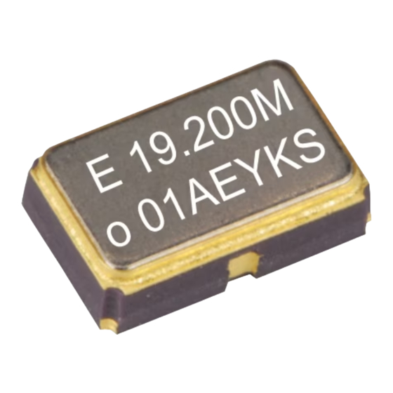
Temperature Compensated Crystal Oscillator (TCXO)
· Package size (5.0 mm × 3.2 mm × 1.45 mm)
· Ultra high stability VC-TCXO
· Output waveform : CMOS
· Reference weight Typ.72 mg
[ 1 ] Product Number / Product Name
(1-1) Product Number / Ordering Code
X1G0053910021xx
last 2 digits code(xx) define Quantity.
The standard is "00", 1 000 pcs/Reel.
(1-2) Product Name / Model Name
TG5032CFN 10.000000 MHz CAGNDA
[ 2 ] Operating range
Parameter
Supply voltage
Frequency control voltage
Operating temperature range
Output load
[ 3 ] Frequency characteristics
( 1 ) Frequency characteristics
Parameter
Output Frequency
Frequency tolerance *1
Frequency / temperature
characteristics
Frequency / load coefficient
Frequency / voltage coefficient
Frequency aging
Holdover stability,
constant temperature
Holdover stability,
constant temperature
Holdover stability
(Free-run accuracy)
*1 Include initial frequency tolerance and frequency deviation after reflow cycles.
*2 Measured in the elapse of 24 hours after reflow soldering.
*3 This includes initial frequency tolerance, frequency / temperature characteristics, frequency / load coefficient, frequency/voltage coefficient and
frequency aging (+25 °C, 20 years) .
( 2 ) Frequency control characteristics
Parameter
Frequency control range
Input impedance
Frequency change polarity
[ 4 ] Electrical characteristics
Parameter
Current consumption
High level output voltage
Low level output voltage
Rise time
Fall time
Symmetry
[ For other general specifications, please refer to the attached Full Data Sheet below ]
Specifications
Symbol
Min.
Typ.
Vcc
3.135
3.3
GND
0
Vc
0.5
1.5
T_use
-40
Load_C
13.5
(Vcc = 3.3 V, GND = 0.0 V, Vc = 1.5 V, Load = 15 pF, T_use = +25 °C)
Specifications
Symbol
Min.
Typ.
fo
-
f_tol
-1.0
fo-Tc
-0.1
fo-Load
-0.1
fo-Vcc
-0.1
-0.5
f_age
-3.0
-
-0.01
-
-0.04
-
-4.6
(Vcc = 3.3 V, GND = 0.0 V, Vc = 1.5 V, Load = 15 pF, T_use = +25 °C)
Specifications
Symbol
Min.
Typ.
-10
f_cont
+5
Zin
100
Positive polarity
-
(Vcc = 3.3 V, GND = 0.0 V, Vc = 1.5 V, Load = 15 pF, T_use = +25 °C)
Specifications
Symbol
Min.
Typ.
Icc
-
Voʜ
90 %
Voʟ
-
tr
-
tf
-
SYM
45
1/21 Page
Unit
Max.
3.465
V
-
0
V
2.5
V
-
+85
°C
15
16.5
pF
Unit
Max.
10
-
MHz
-
+1.0
x10⁻⁶
-
+0.1
x10⁻⁶
-
+0.1
x10⁻⁶
-
+0.1
x10⁻⁶
-
+0.5
x10⁻⁶
-
+3.0
x10⁻⁶
-
+0.01
x10⁻⁶
-
+0.04
x10⁻⁶
-
+4.6
x10⁻⁶
Unit
Max.
-
-5
x10⁻⁶
-
+10
x10⁻⁶
kΩ
-
-
-
Unit
Max.
-
5.0
mA
-
-
V
-
10 %
V
-
8.0
ns
-
8.0
ns
-
55
%
Conditions
-
-
Vc = 1.5 ±1.0 V
-
-
Conditions
-
T_use = +25 °C ±2 °C
After 2 reflows *2
T_use = -40 °C to +85 °C
(Reference to (fmax+fmin)/2)
Load ±10 %
Vcc ±5 %
T_use = +25 °C first year
T_use = +25 °C 20 years
T_use = +25 °C, 24 hours
(after 10 days of continuous
operation)
T_use = +25 °C, 24 hours
(after 48 hours of continuous
operation)
*3
Conditions
Vc = 0.5 V
Vc = 2.5 V
Vc = 1.5 V
-
Conditions
-
-
-
10 % Vcc to 90 % Vcc level
90 % Vcc to 10 % Vcc level
50 % Vcc Level
No.: TG5032CFN ver1.0
Advertisement

Related Manuals for Seiko Epson TG5032CFN

Summary of Contents for Seiko Epson TG5032CFN
- Page 1 [ 1 ] Product Number / Product Name (1-1) Product Number / Ordering Code X1G0053910021xx last 2 digits code(xx) define Quantity. The standard is "00", 1 000 pcs/Reel. (1-2) Product Name / Model Name TG5032CFN 10.000000 MHz CAGNDA [ 2 ] Operating range Specifications Symbol Unit Conditions Parameter Min.
- Page 2 Ultra high stability temperature compensated crystal oscillator Product name : TG5032CFN / TG5032SFN Features ⚫ Ultra high stability (< 0.1 x 10 ⚫ Low phase noise ⚫ Frequency range : 10 MHz to 40 MHz ⚫ Output : CMOS, Clipped sine wave ⚫...
- Page 3 1. Product Number / Product Name (1-1) Product Number / Ordering Code TG5032CFN: X1G005391xxxx00 (Please contact Epson for details of number xxxx) TG5032SFN: X1G005401xxxx00 (The last 2 digits code (00) define Quantity. 1 000 pcs/Reel) (1-2) Product Name / Model Name (Standard form) T G 5 0 3 2 C F N 10.000000MHz C A G N D A...
-
Page 4: Operating Conditions
2. Electrical characteristics 1) Absolute maximum ratings Parameter Symbol Unit Min. Typ. Notes Supply voltage -GND -0.5 +4.0 C Storage temperature T_stg Store as bare product after packing Frequency control voltage -GND -0.5 +0.5 Terminal 2) Operating conditions Parameter Symbol Unit Min. -
Page 5: Electrical Characteristics
3-2) Frequency control characteristics = Typ., GND = 0.0 V, Vc = Typ. V, Load = Typ., T_use = +25 °C) Parameter Symbol Unit Min. Typ. Notes -10.0 -5.0 Frequency control range f_cont Vc = 1.5 V±1.0 V, Vc = 1.65 V±1.0 V ×... - Page 6 3. Characteristics 3-1) “Frequency / Temperature Characteristics” 3-1-1) Standard spec : ±0.1 × 10 Max. (T_use = -40 °C to +85 °C) 19.2 MHz [N = 40 pcs] Temperature [°C] Temperature [°C] 30.72 MHz [N = 40 pcs] Temperature [°C] Temperature [°C] 40 MHz [N = 40 pcs] Temperature [°C]...
- Page 7 3-2) Frequency Aging (40 MHz) [N = 5 pcs] * Aging is estimated from environmental reliability tests and the expected amount of frequency variation over time. It is not intended as a guarantee of performance over the product-life cycle. 3-3) Holdover Stability (19.2 MHz) [N = 40 pcs] 3-4) Frequency Control Characteristics [N = 40 pcs] No.: TG5032xFN_AE_Ver.
- Page 8 3-5) Current Consumption 3-6) Rise time / Fall time (at CMOS output) 3-7) Output voltage [V ] (at CMOS output) 3-8) Symmetry (at CMOS output) 2-9) Output level [V ] (at Clipped sine wave) No.: TG5032xFN_AE_Ver. 1.07 8/21 Page...
- Page 9 3-10) Start up time (19.2 MHz, 40 MHz) 19.2 MHz 40 MHz No.: TG5032xFN_AE_Ver. 1.07 9/21 Page...
- Page 10 3-11) Phase noise (10 MHz, 19.2 MHz, 20 MHz) [N = 25 pcs] 10 MHz 19.2 MHz 20 MHz No.: TG5032xFN_AE_Ver. 1.07 10/21 Page...
- Page 11 3-11) Phase noise (25 MHz, 30.72 MHz, 40 MHz) [n = 25 pcs] 25 MHz 30.72 MHz 40 MHz No.: TG5032xFN_AE_Ver. 1.07 11/21 Page...
- Page 12 3-12) Short term stability [ADEV] (19.2 MHz) TCXO mode 3-13) TDEV (19.2 MHz, Loop BW = 0.1 Hz) Constant temperature : +25 °C Constant temperature : +70 °C 3-14) MTIE (19.2 MHz, Loop BW = 0.1 Hz) Constant temperature : +25 °C Constant temperature : +70 °C Compliant with G.813 option1 and 2 No.: TG5032xFN_AE_Ver.
- Page 13 4-2) Soldering pattern Example of patterning design indicated as follows. In an actual design, please consider mounting density, the reliability of soldering, etc. and check whether performance is optimal. Soldering pattern of TG5032CFN / SFN unit : mm Please set By-pass capacitor (0.1μF) near the Vcc pad...
-
Page 14: Timing Chart
5. Timing chart 5-1) Output waveform (CMOS output) 90 % V 50 % V 10 % V SYM=tw/t×100 % 5-2) Output waveform (Clipped sine wave output) SYM=tw/t×100 % No.: TG5032xFN_AE_Ver. 1.07 14/21 Page... - Page 15 6. Test circuit 6-1) CMOS output for TCXO 1) Output Load : 15 pF Test Point N.C. Supply By-pass Load_C Voltage Capacitor 15 pF 2) Current consumption N.C. Supply By-pass Load_C Voltage Capacitor 15 pF 3) Conditions Min. 1 MΩ 1.
- Page 16 6-2) CMOS output for VC-TCXO 1) Output Load : 15 pF Test Point Supply By-pass Load_C Voltage Capacitor 15 pF Control Voltage 2) Current consumption Supply By-pass Load_C Voltage Capacitor 15 pF Control Voltage 3) Conditions Min. 1 MΩ 1.
- Page 17 1) Output Load : 10 kΩ // 10 pF DC-cut Capacitor 0.01 Test Point N.C. By-pass Capacitor Load_R Load_C Supply 10 kΩ 10 pF Voltage 2) Current consumption DC-cut Capacitor 0.01 N.C. By-pass Capacitor Load_C Load_R Supply 10 pF 10 kΩ...
- Page 18 6-4) Clipped sine wave output for VC-TCXO 1) Output Load : 10 kΩ // 10 pF DC-cut Capacitor 0.01 Test Point Supply By-pass Voltage Capacitor Load_C Load_R 10 kΩ 10 pF Control Voltage 2) Current consumption DC-cut Capacitor ...
-
Page 19: Reflow Profile
Time [ s ] 8. Packing information (8-1) Product number last 2 digits code (00) define Quantity. 1 000 pcs/Reel. TG5032CFN: X1G005391xxxx00 (Please contact Epson for details of number xxxx) TG5032SFN: X1G005401xxxx00 (8-2) Taping specification Subject to EIA-481 IEC-60286 JIS C0806... - Page 20 Moisture Sensitivity Level, Electro-Static Discharge (9-1) Moisture Sensitivity Level (MSL) Parameter Specifications Conditions LEVEL1 JEDEC J-STD-020D (9-2) Electro-Static Discharge (ESD) Parameter Specifications Conditions EIAJ ED-4701-1 C111A, 100 pF, 1.5 kΩ, 3 times Human Body Model (HBM) 2 000 V Min EIAJ ED-4701-1 C111, 200 pF, 0 Ω, 1 time Machine Model (MM) 200 V Min...
- Page 21 10. Handling precautions Prior to using this product, please carefully read the section entitled “Precautions” on our Web site https://www5.epsondevice.com/en/information/#precaution ) for instructions on how to handle and use the product properly to ensure optimal performance of the product in your equipment. Before using the product under any conditions other than those specified therein, please consult with us to verify and confirm that the performance of the product will not be negatively affected by use under such conditions.
Need help?
Do you have a question about the TG5032CFN and is the answer not in the manual?
Questions and answers