Table of Contents
Advertisement
Quick Links
DVD-S42EE / DVD-S42GC / DVD-S42GCA / DVD-S42GCS /
SPECIFICATIONS
PDF created with pdfFactory Pro trial version
DVD-S42GCU / DVD-S42PL / DVD-S42PLA
Specifications
Power supply:
Power consumption:
Power consumption in standby mode:
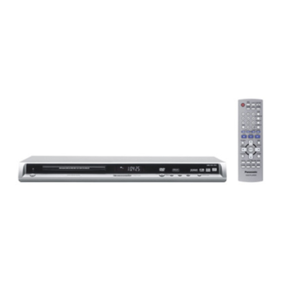
Dimensions:
Mass:
Signal system:
Operating temperature range:
Operating humidity range:
Discs played [8 cm (3") or 12 cm (5")]:
(1)
DVD (DVD-Video, DivX*6,7)
(2)
DVD-RAM (DVD-VR, JPEG*4,7, MPEG4*5,7, DivX*6,7,
MP3*2,7)
(3)
DVD-R (DVD-Video, DVD-VR, JPEG*4,7, MP3*2,7, DivX*
6,7, MPEG4*5,7)
(4)
DVD-R DL (DVD-Video, DVD-VR)
www.pdffactory.com
ORDER NO.CHM0603009CE
DL4.1 Mechanism Series
(S).......................Silver Type
AC230 V, 50 Hz
(DVD-S42EE)
AC110-240 V, 50/60 Hz
(DVD-S42GC/GCA/GCU/GCS/
PL)
AC120 V, 60 Hz
(DVD-S42PLA)
11 W
1 W (approx.)
430 (W) × 251 (D) × 43 (H) mm
2.2 kg (approx.)
PAL 625/50, PAL 525/60, NTSC
(DVD-S42EE/GC/GCA/GCS/
GCU)
NTSC
(DVD-S42PLA/PL)
+ 5 to + 35 °C
5 to 90 % RH (no
condensation)
1
DVD Player
Color
Advertisement
Table of Contents

Related Manuals for Panasonic DVD-S42EE


Summary of Contents for Panasonic DVD-S42EE
- Page 1 ORDER NO.CHM0603009CE DVD Player DVD-S42EE / DVD-S42GC / DVD-S42GCA / DVD-S42GCS / DVD-S42GCU / DVD-S42PL / DVD-S42PLA DL4.1 Mechanism Series Color (S).......Silver Type SPECIFICATIONS Specifications Power supply: AC230 V, 50 Hz (DVD-S42EE) AC110-240 V, 50/60 Hz (DVD-S42GC/GCA/GCU/GCS/ AC120 V, 60 Hz...
- Page 2 (Sub sampling is 4:0:0, 4:2:2, 4:2:0, 4:4:4) Extremely long and slender pictures may not be displayed. MPEG4 data recorded with the Panasonic SD multi cameras or DVD video recorders conforming to SD VIDEO specifications (ASF standard) /MPEG4 (Simple Profile) video system/G.726 audio system...
- Page 3 PAL: (576)p/(576)i] (DVD-S42EE/GC/GCA/GCS/GCU) [NTSC: (480)p/(480)i] (DVD-S42PL/PLA) Y output level: 1 Vp-p (75 P B output level: 0.7 Vp-p (75 P R output level: 0.7 Vp-p (75 Output terminal: Pin jack (Y: green, P B : blue, P R : red)
-
Page 4: Important Service Information
Solder: This model uses lead free solder (PbF). 2006 Matsushita Electric Industrial CO., Ltd. All rights reserved. Unauthorized copying and distribution is a violation of law. 1. IMPORTANT SERVICE INFORMATION 1.1. Notes When you replace EEPROM or exchange MODULE P.C.B., you have to take "Manual for customer"... -
Page 5: About Divx
Please don't forget take it to the customer with unit! 1.2. About DivX 1.2.1. DivX A video compression format developed by DivXNetworks, Inc. that compresses video files without any considerable loss of video quality. 1.2.2. About DivX Video-on-Demand Content PDF created with pdfFactory Pro trial version www.pdffactory.com... - Page 6 PDF created with pdfFactory Pro trial version www.pdffactory.com...
-
Page 7: Safety Precautions
1.3. Manual for Customer 2. SAFETY PRECAUTIONS 2.1. GENERAL GUIDELINES 1. When servicing, observe the original lead dress. If a short circuit is found, replace all parts which have been overheated or damaged by the short circuit. 2. After servicing, see to it that all the protective devices such as insulation barriers, insulation papers shields are properly installed. -
Page 8: Prevention Of Electro Static Discharge
1. Plug the AC cord directly into the AC outlet. Do not use an isolation transformer for this check. 2. Connect a 1.5k , 10 watts resistor, in parallel with a 0.15 capacitors, between each exposed metallic part on the set and a good earth ground such as a water pipe, as shown in Figure 3. -
Page 9: Precaution Of Laser Diode
assembly. 3. Use only a grounded-tip soldering iron to solder or unsolder ES devices. 4. Use only an anti-static solder removal device. Some solder removal devices not classified as "anti-static (ESD protected)" can generate electrical charge sufficient to damage ES devices. 5. -
Page 10: Service Caution Based On Legal Restrictions
5. SERVICE CAUTION BASED ON LEGAL RESTRICTIONS 5.1. General description about Lead Free Solder (PbF) The lead free solder has been used in the mounting process of all electrical components on the printed circuit boards used for this equipment in considering the globally environmental conservation. -
Page 11: Prevention Of Static Electricity Discharge
for which the lead free solder is used. (Definition: The letter of “PbF” is printed on the PCB using the lead free solder.) - To put lead free solder, it should be well molten and mixed with the original lead free solder. - Remove the remaining lead free solder on the PCB cleanly for soldering of the new IC. -
Page 12: Disassembling The Casing And Checking P.c.b.s
form your body. 6.1.3. Handling of optical pickup 1. To keep the good quality of the optical pickup maintenance parts during transportation and before installation, the both ends of the laser diode are short-circuited. After replacing the parts with new ones, remove the short circuit according to the correct procedure. - Page 13 7.2. Casing Parts and P.C.B. Positions 7.3. Top Panel 1. Unscrew the screws. PDF created with pdfFactory Pro trial version www.pdffactory.com...
- Page 14 7.4. Front Panel 1. Release the tabs and connector. 2. Release the tabs. 7.5. Operation P.C.B. and Power SW P.C.B. 1. Unscrew the screws. PDF created with pdfFactory Pro trial version www.pdffactory.com...
- Page 15 7.6. Module P.C.B. 1. Remove the connectors. 2. Unscrew the screws. 3. Press each tab with the nipper to module PCB vertically. 7.7. Mechanism Unit 1. Unscrew the screws. 2. Release the tabs. PDF created with pdfFactory Pro trial version www.pdffactory.com...
- Page 16 7.8. Rear panel 1. Unscrew the screws. 2. Release the tabs. 7.9. Mother P.C.B. 1. Unscrew the screws. PDF created with pdfFactory Pro trial version www.pdffactory.com...
-
Page 17: Service Position
7.10. Service Position 7.10.1. Servicing position of the Module P.C.B. 7.10.2. Servicing position of the Mother P.C.B. PDF created with pdfFactory Pro trial version www.pdffactory.com... -
Page 18: Assembling And Disassembling The Mechanism Unit
7.10.3. List of the Extension Cables 8. ASSEMBLING AND DISASSEMBLING THE MECHANISM UNIT 8.1. Disassembly Procedure PDF created with pdfFactory Pro trial version www.pdffactory.com... - Page 19 8.2. Traverse Unit 1. Slide the lever (A) in the arrow direction (to the opposite side) till it stops. 2. Slide the lever (A) further by bending the tab at the right side of the lever A in the right direction. (The right groove opens and the boss becomes seen.) 3.
- Page 20 4. Remove the traverse unit 8.3. Tray 1. Slide the guide tray unit while pressing the stopper in the arrow direction, and remove the guide tray unit. PDF created with pdfFactory Pro trial version www.pdffactory.com...
- Page 21 2. Raise the loading unit. 3. Slide the lever in the arrow direction till it stops and pull the tray out. 4. Spread the tabs at the both sides and pull the tray out. (The tray slides a little forward and stops.) PDF created with pdfFactory Pro trial version www.pdffactory.com...
- Page 22 5. Remove the drive arm concave phase from the tray slider and tray. <Assembling the tray unit> 1. Insert a part of the tray into the unit sliding over the groove on the mechanical chassis unit. 2. Insert the tray to the point before the tab of the mechanical chassis unit.
- Page 23 8.4. Loading section 1. Spread the tabs at the both sides and push out the drive arm shaft. 2. Hook the lock lever spring on the lock lever projection part temporarily. 3. Unlock the tab and remove the lock lever. PDF created with pdfFactory Pro trial version www.pdffactory.com...
- Page 24 4. Remove the belt. 5. Unlock the tab and remove the pulley. 6. Remove the relay gear. 7. Turn the change lever in the arrow direction till it stops. 8. Hook the change lever spring on the change lever project part temporarily.
- Page 25 9. Pull the lever (B) in the bottom side to your side and remove the change lever. 10. Remove the drive rack, the sub rack and the drive gear. 8.5. Loading motor P.C.B. PDF created with pdfFactory Pro trial version www.pdffactory.com...
-
Page 26: Optical Pickup Unit
1. Unscrew the screws. 8.6. Optical Pickup Unit 8.6.1. Cautions to Be Taken in Handling the Optical Pickup Unit The laser diode in the optical pickup unit may be damaged due to electrostatic discharge generating from clothes or human body. Use due caution to electrostatic discharge damage when servicing the laser diode. - Page 27 8.6.2. Procedure for Disassembling the Optical Pickup Unit 1. Move the optical pickup unit in the arrow direction till it stops. 2. Unscrew the screws. PDF created with pdfFactory Pro trial version www.pdffactory.com...
- Page 28 3. Remove the drive rack. 4. Unscrew the screw. 5. Slide the shaft in the arrow direction. 6. Lift the optical pickup unit with the shaft. PDF created with pdfFactory Pro trial version www.pdffactory.com...
- Page 29 7. Remove the optical pickup unit. 8. Pull the shaft and the rubber out. <Assembling the optical pickup unit> PDF created with pdfFactory Pro trial version www.pdffactory.com...
- Page 30 1. Pass the intermediate FPC through the frame hole. 2. Align the guide section of the optical pickup unit with the rail. 3. Install the shaft top to the holder. 4. The intermediate FFC is fixed as shown below. 8.7. Traverse Motor 1.
- Page 31 2. Remove the cover while lifting the inner gear. 3. Remove the solders. 4. Remove the traverse motor. PDF created with pdfFactory Pro trial version www.pdffactory.com...
-
Page 32: Self-Diagnosis Function And Service Modes
9. SELF-DIAGNOSIS FUNCTION AND SERVICE MODES 9.1. Optical Pickup Breakdown Diagnosis The optical pickup self-diagnosis function and tilt adjustment check function have been included in this unit. When repairing, use the following procedure for effective Self-diagnosis and tilt adjustment.Be sure to use the self-diagnosis function before replacing the optical pickup when "NO DISC"... -
Page 33: Service Mode Table
9.2. Service Mode Table 1 The service modes can be activated by pressing various button combination on the player and remote control unit. PDF created with pdfFactory Pro trial version www.pdffactory.com... -
Page 34: Dvd Self Diagnostic Function-Error Code
Player buttons Remote control unit Application Note buttons PAUSE Displaying the UHF display F_ _ _ Refer to 9.3. Self- Diagnosis OPEN/CLOSE Function Display). Jitter check, tilt adjustment Refer to 11.4. Optical *Display shows J_xxx/yyy_zz Pickup Tilt "yyy" and "zz" shown to the right have nothing Adjustment to do with the jitter value. - Page 35 Error Error Content Additional error explanation Defect 1 Defect 2 Code U, H error Focus error Unfinalized DVD- Tray loading error Spindle servo (Spindle servo, DV3.2 (IC8001) SP error motor, CLV servo error) Traverse servo error Tracking servo error Seek error Power error Cannot switch off the power because of the panel and system...
- Page 36 Error Error Content Additional error explanation Defect 1 Defect 2 Code F601 Indeterminate Operation stopped caused by the DV3.2 sector ID request to access abnormal ID data (IC8001) requested F602 Access failure to LEAD IN data unreadable LEAD-IN caused by demodulation error F603 Access failure to...
-
Page 37: Last Error Code Saved During No Play
Error Error Content Additional error explanation Defect 1 Defect 2 Code F890 Sending Sending message to AV task message when message is being sent to AV task F891 Message couldn’t Begin sending message to AV task be sent to AV task F893 FROM... - Page 38 Error Error Content System computer Setting task System computer internal code error code F0BF 6) Cannot playback PCND_NOPLAY 0xDOBF DriveManager because physical layer is PHYSICAL 0x50 not recoginizable F0C0 8) DVD: Cannot playback PCND_NOPLAY VIDEO DiscManager 0xDOC0 because it is not DVD 0x70 Video/Adio/VR F0C1...
- Page 39 PDF created with pdfFactory Pro trial version www.pdffactory.com...
-
Page 40: Sales Demonstration Lock Function
9.6. Sales demonstration lock function This function prevents discs from being lost when the unit is used for sales demonstrations by disabling the disc eject function. "LOC" is displayed on the unit, and ordinary operation is disabled. 9.6.1. Setting PDF created with pdfFactory Pro trial version www.pdffactory.com... -
Page 41: Handling After Completing Repairs
The sales demonstration lock is set by simultaneously pressing STOP button on the player and POWER button on the remote control unit for 1 second or longer. 9.6.2. Cancellation The lock can be cancelled by the same procedure as used in setting. ("UNLOC" is displayed on cancellation. -
Page 42: Adjustment Procedures
- The firmware of the DVD player may be renewed to improve the quality including operationability and playerbility to the substandard discs.processing to optimize the drive. The recovery disc has also firmware version-up. - After version-up, recovery processing is executed automatically. - Part number of the recovery disc for version-up will be noticed when it is supplied. -
Page 43: Important Points In Adjustment
Application Name Number Tilt adjustment DVD test disc DVDT-S15 or DVDT-S01 TORX screw driver (T6) Available on sales route. (T6) or RFKZ0185 Inspection Extension cable (module P.C.B. to mother VUC8026 P.C.B.) Extension cable (module P.C.B. to mother RFKZ0106 P.C.B.) Others Hanarl VFK1784 Grease... -
Page 44: Optical Adjustment
2. Handle discs carefully in order to maintain their flatness. Place them into their case after use and store them vertically. Store discs in a cool place where they are not exposed to direct sunlight or air from air conditioners. 3. - Page 45 6. Adjust tilt adjustment screw 1 so that the jitter value is minimized. 7. Play test disc T30 (central periphery). 8. Adjust tilt adjustment screw 2 so that the jitter value is minimized. 9. Repeat adjusting tilt adjustment screws 1 and 2 alternately until the jitter value is minimized.
- Page 46 11.4.1.3. Check after adjustment Play test disc or any other disc to make sure there is no picture degradation in the inner, middle and outer peripheries, and no audio skipping. After adjustment is finished, lock each adjustment screw in position using screw lock. 11.4.1.4.
- Page 47 mechanism unit in this sequence. 2. Lay the mechanism unit upside down, and fix adjustment scwer with screw lock. 3. After fixing, reassemble mechanism unit, rear panel, front panel and top panel. It is also possible to perform screw lock on the head of an adjustment screw after an adjustment end using an injector etc.
- Page 48 INITIAL/LOGO ABBREVIATIONS A0~UP ADDRESS ACLK AUDIO CLOCK AD0~UP ADDRESS BUS ADATA AUDIO PES PACKET DATA ADDRESS LATCH ENABLE AMUTE AUDIO MUTE AREQ AUDIO PES PACKET REQUEST AUDIO RF SERVO AMP INVERTED INPUT SERVO AMPOUTPUT ASYNC AUDIO WORD DISTINCTION SYNC BIT CLOCK (PCM) BCKIN BIT CLOCK INPUT BLACK DROP OUT...
- Page 49 INITIAL/LOGO ABBREVIATIONS DACCK D/A CONVERTER CLOCK DEEMP DEEMPHASIS BIT ON/OFF DEMPH DEEMPHASIS SWITCHING DIG0~UP FL DIGIT OUTPUT DATA INPUT DMSRCK DM SERIAL DATA READ CLOCK DMUTE DIGITAL MUTE CONTROL DROP OUT DOUT0~UP DATAOUTPUT DATA SLICE RF (BIAS) DROP OUT SIGNAL DRPOUT DATA REQUEST DREQ...
- Page 50 INITIAL/LOGO ABBREVIATIONS IECOUT IEC958 FORMAT DATA OUTPUT IPFRAG INTERPOLATION FLAG IREF I (CURRENT) REFERENCE ISEL INTERFACE MODE SELECT LDON LASER DIODE CONTROL LASER POWER CONTROL LRCK L CH/R CH DISTINCTION CLOCK MA0~UP MEMORY ADDRESS MEMORY CLOCK MCKI MEMORY CLOCK INPUT MCLK MEMORY SERIAL COMMAND CLOCK...
- Page 51 INITIAL/LOGO ABBREVIATIONS READ ENABLE RFENV RF ENVELOPE RF PHASE DIFFERENCE OUTPUT (CD-ROM) REGISTER SELECT RSEL RF POLARITY SELECT RESET RESERVE SBI0, 1 SERIAL DATA INPUT SBO0 SERIAL DATA OUTPUT SBT0, 1 SERIAL CLOCK SERIAL DATA CLOCK SCKR AUDIO SERIAL CLOCK RECEIVER SERIAL CLOCK SCLK...
- Page 52 SUB CODE Q DATA SYSCLK SYSTEM CLOCK INITIAL/LOGO ABBREVIATIONS TRACKING ERROR TIBAL BALANCE CONTROL BALANCE OUTPUT 1 BALANCE INPUT BALANCE INPUT BALANCE OUTPUT 2 TPSN OP AMP INPUT TPSO OP AMP OUTPUT TPSP OP AMP INVERTED INPUT TRCRS TRACK CROSSSIGNAL TRON TRACKING ON TRSON...
-
Page 53: Voltage Chart
INITIAL/LOGO ABBREVIATIONS X' TAL XALE X ADDRESS LATCH ENABLE XAREQ X AUDIO DATA REQUEST XCDROM X CD ROM CHIP SELECT X CHIP SELECT XCSYNC X COMPOSITE SYNC X DATA STROBE XHSYNCO X HORIZONTAL SYNC OUTPUT XHINT XH INTERRUPTREQUEST X' TAL OSCILLATOR INPUT XINT X INTERRUPT X MEMORY WRITE ENABLE... -
Page 54: Interconnection Schematic Diagram & Schematic Diagram Notes
14.1. OVERALL BLOCK DIAGRAM 14.2. POWER SUPPLY BLOCK DIAGRAM 14.3. SERVO BLOCK DIAGRAM 14.4. VIDEO BLOCK DIAGRAM (DVD-S42GC/GCA/GCS/GCU/PL/PLA) 14.5. VIDEO BLOCK DIAGRAM (DVD-S42EE) 14.6. AUDIO BLOCK DIAGRAM 15. INTERCONNECTION SCHEMATIC DIAGRAM & SCHEMATIC DIAGRAM NOTES 15.1. INTERCONNECTION SCHEMATIC DIAGRAM 15.2. SCHEMATIC DIAGRAM NOTES This schematic diagram may be modified at any time with the development of new technology. -
Page 55: Print Circuit Board
16.4. FRONT & AV OUT SECTION (MOTHER P.C.B. (2 / 2)) SCHEMATIC DIAGRAM (DVD-S42GC/GCA/GCS/GCU/PL/PLA) 16.5. MODULE SCHEMATIC DIAGRAM 17. PRINT CIRCUIT BOARD 17.1. MOTHER P.C.B. (DVD-S42EE) 17.2. MOTHER P.C.B. (DVD-S42GC/GCA/GCS/GCU/PL/PLA) 17.3. MOTHER P.C.B. ADDRESS INFORMATION 17.4. MODULE P.C.B. (1/2) 17.5. MODULE P.C.B. (2/2) 17.6. - Page 56 18.2. MECHANISM SECTION EXPLODED VIEW PDF created with pdfFactory Pro trial version www.pdffactory.com...
- Page 57 18.3. PACKING & ACCESSORIES SECTION EXPLODED VIEW PDF created with pdfFactory Pro trial version www.pdffactory.com...
-
Page 58: Replacement Parts List
19. REPLACEMENT PARTS LIST Notes: *Important safety notice: Components identified by mark have special characteristics important for safety. Furthermore, special parts which have purposes of fire-retardant (resistors), high-quality sound (capacitors), low-noise (resistors), etc. are used. When replacing any of components, be sure to use only manufacture’s specified parts shown in the parts list. - Page 59 Ref. No. Part No. Part Name & Description Remarks VEP76129AT MODULE P.C.B. (RTL) EE/GC/GCA/PL/PLA VEP76129ET MODULE P.C.B. (RTL) GCS/GCU VEP76126B MOTHER P.C.B. (RTL) GC/GCA VEP76126C MOTHER P.C.B. (RTL) EE VEP76126K MOTHER P.C.B. (RTL) GCS/GCU VEP76126L MOTHER P.C.B. (RTL) PL VEP76127A MOTHER P.C.B.
- Page 60 Ref. No. Part No. Part Name & Description Remarks RGQC0054 DUSTPROOF SHEET RHD26046 SCREW RHD26046 SCREW RHD26046 SCREW RHD26046 SCREW RHD26046 SCREW RHD26046 SCREW VEP70131A FRONT P.C.B. (RTL) 55-1 REZ1709 CABLE (3P) 55-2 REZ1708 CABLE (5P) VEP70132A SW P.C.B. (RTL) RHD30007-1SJ SCREW RHD30007-1SJ...
- Page 61 RMA1890 MAGNET HOLDER Ref. No. Part No. Part Name & Description Remarks RMR1686-K CLAMP PLATE RGQ0417-K TRAY RME0353-1 TRAY SLIDER SPRING RML0631 TRAY SLIDER XQN17+C25FJ SCREW XTB26+6GFJ SCREW XTN2+6GFJ SCREW RMQ1280 FFC HOLDER PIECE EUR7631190R REMOTE CONTROL ASS’Y PL/PLA EUR7631200R REMOTE CONTROL ASS’Y EE/GC/GCA/GCS/GCU A1-1...
- Page 62 Ref. No. Part No. Part Name & Description Remarks C1102 ECQB1H104JF4 50V 0.1U EE/GC/GCA/GCS/GCU/PL C1110 F1H1H102A798 50V 1000P C1111 F2A1A681A539 10V 680U C1112 F2A1A102A206 10V 1000U C1115 ECJ1VF1C104Z 16V 0.1U C1116 F2A1A221A206 10V 220U C1117 F2A0J102A247 6.3V 1000U C1121 F2A0J681A550 6.3V 680U C1122 F2A0J222A247...
- Page 63 Ref. No. Part No. Part Name & Description Remarks C4315 F1H1C104A090 16V 0.1U C4323 F2A1V221A082 35V 220U C4324 F2A1V221A082 35V 220U C4336 F1H1H820A799 50V 82P C4337 F1H1H820A799 50V 82P C4414 F2A1E470A205 25V 47U C4415 F2A1E470A205 25V 47U C4423 ECJ1VC1H102J 50V 1000P C4427 ECJ1VC1H102J 50V 1000P...
- Page 64 Ref. No. Part No. Part Name & Description Remarks C8053 F1G1C104A042 16V 0.1U C8054 ECJ0EC1H221J 50V 220P C8055 ECJ1VB0J105K 6.3V 1U C8056 ECJ0EB1E222K 25V 2200P C8057 ECJ1VB0J105K 6.3V 1U C8111 F1G1A104A014 10V 0.1U C8112 ECJ1VB0J105K 6.3V 1U C8113 ECJ0EB1E471K 25V 470P C8151 ECJ2FB0J106K 6.3V 10U...
- Page 65 Ref. No. Part No. Part Name & Description Remarks C8521 F1G1A104A014 10V 0.1U C8522 F1G1A104A014 10V 0.1U C8523 F1G1C104A042 16V 0.1U C8524 F1G1C104A042 16V 0.1U C8525 F1G1C562A040 16V 5600P C8526 F1G1C183A004 16V 0.018U C8527 F1G1C333A004 16V 0.033U C8528 ECJ1VB0J105K 6.3V 1U C8529 ECJ1VB0J105K 6.3V 1U...
- Page 66 Ref. No. Part No. Part Name & Description Remarks D1152 B0JAMG000031 DIODE D1152 B0JAMK000023 DIODE EE/GC/GCA/GCS/GCU/PL D1153 B0EAKM000122 DIODE D1171 B0JAME000037 DIODE D3821 MA3X152A0L DIODE D4301 MAZ40560HF DIODE D6081 MAZ40910LF ZENER DIODE D6101 LNJ201LPQJA D8211 MA2J11100L DIODE D8571 MA2J72800L DIODE DP6081 A2BA00000229 FL DISPLAY SCREEN...
- Page 67 PDF created with pdfFactory Pro trial version www.pdffactory.com...
- Page 68 Ref. No. Part No. Part Name & Description Remarks K3501 ERJ3GEY0R00V 1/10W 0 GC/GCA/GCS/GCU/PL/PLA K3505 ERJ3GEY0R00V 1/10W 0 K3810 ERJ3GEY0R00V 1/10W 0 K3811 ERJ3GEY0R00V 1/10W 0 K3813 ERJ3GEY0R00V 1/10W 0 K3872 ERJ3GEY0R00V 1/10W 0 K6001 ERJ3GEY0R00V 1/10W 0 K6008 ERJ3GEY0R00V 1/10W 0 K8101 ERJ3GEY0R00V...
- Page 69 LB8257 ERJ3GEY0R00V 1/10W 0 Ref. No. Part No. Part Name & Description Remarks LB8258 ERJ3GEY0R00V 1/10W 0 LB8259 ERJ3GEY0R00V 1/10W 0 LB8260 ERJ3GEY0R00V 1/10W 0 LB8261 ERJ2GE0R00X 1/16W 0 LB8262 ERJ2GE0R00X 1/16W 0 LB8301 J0JBC0000042 COIL LB8302 J0JBC0000042 COIL LB8303 J0JBC0000042 COIL LB8304...
- Page 70 Ref. No. Part No. Part Name & Description Remarks Q4751 B1ABDF000033 TRANSISTOR Q6085 B1ABGC000011 TRANSISTOR Q8551 B1ABDF000018 TRANSISTOR Q8552 B1ADGB000008 TRANSISTOR Q8561 B1ABDF000018 TRANSISTOR Q8562 B1ADGB000008 TRANSISTOR QR1115 B1GBCFNN0043 TRANSISTOR QR3501 B1GBCFLL0043 TRANSISTOR QR3502 B1GBCFLL0043 TRANSISTOR QR3821 B1GBCFLL0043 TRANSISTOR QR3822 B1GBCFLL0043 TRANSISTOR QR3823...
- Page 71 Ref. No. Part No. Part Name & Description Remarks R3535 ERJ3GEYJ750V 1/10W 75 R3536 ERJ3GEYJ750V 1/10W 75 R3821 ERJ3GEYJ223V 1/10W 22K R3822 ERJ3GEYJ223V 1/10W 22K R3823 ERJ3GEYJ472V 1/10W 4.7K R3824 ERJ3GEYJ223V 1/10W 22K R3825 ERJ3GEYJ472V 1/10W 4.7K R3826 ERJ3GEYJ183V 1/10W 18K R3827 ERJ3GEYJ223V 1/10W 22K...
- Page 72 Ref. No. Part No. Part Name & Description Remarks R6024 ERJ3GEY0R00V 1/10W 0 EE/GC/GCA/PL/PLA R6025 ERJ3GEYJ103V 1/10W 10K R6026 ERJ3GEYJ472V 1/10W 4.7K R6026 ERJ3GEYJ472V 1/10W 2.7K GCA/GC/GCS/GCU R6026 ERJ3GEYJ472V 1/10W 1.2K PLA/PL R6040 ERJ3GEYJ103V 1/10W 10K R6050 ERJ3GEYJ103V 1/10W 10K R6060 ERJ3GEYJ103V 1/10W 10K...
- Page 73 Ref. No. Part No. Part Name & Description Remarks R8531 ERJ2GEJ152X 1/16W 1.5K R8532 ERJ2GEJ222X 1/16W 2.2K R8533 ERJ2GE0R00X 1/16W 0 R8541 ERJ2GEJ153X 1/16W 15K R8551 ERJ2GE0R00X 1/16W 0 R8552 ERJ2GEJ102X 1/16W 1K R8553 ERJ2GEJ102X 1/16W 1K R8554 ERJ2GEJ680X 1/16W 68 R8555 ERJ2GEJ2R2X 1/16W 2.2...
- Page 74 Ref. No. Part No. Part Name & Description Remarks S6162 EVQ11G05R SWITCH S6171 EVQ11G05R SWITCH S6172 EVQ11G05R SWITCH T1021 G4D2A0000265 TRANSFORMER VA1002 ERZVA5Z471 TRANSIENT/SURGE ABSORBER W220 ERJ3GEY0R00V 1/10W 0 W221 ERJ3GEY0R00V 1/10W 0 W222 ERJ3GEY0R00V 1/10W 0 W223 ERJ3GEY0R00V 1/10W 0 W224 ERJ3GEY0R00V 1/10W 0...
-
Page 75: Schematic Diagram For Printing With A4
ZA4751 K4CZ01000027 TERMINAL Ref. No. Part No. Part Name & Description Remarks ZA4754 RMCC0027 TERMINAL 20. SCHEMATIC DIAGRAM FOR PRINTING WITH A4 FLE060300006JA PDF created with pdfFactory Pro trial version www.pdffactory.com... - Page 76 Ref No. IC8001 MODE PLAY STOP Ref No. IC8001 MODE PLAY STOP Ref No. IC8001 MODE PLAY STOP Ref No. IC8001 MODE PLAY STOP Ref No. IC8001 MODE PLAY STOP Ref No. IC8001 MODE PLAY STOP Ref No. IC8001 MODE PLAY STOP Ref No.
- Page 77 IC8651(EE/GC/GCA/PL/PLA) Ref No. MODE PLAY STOP Ref No. IC8651(GCS/GCU) MODE PLAY STOP IC8651(GCS/GCU) Ref No. MODE PLAY STOP Q8551 Q8552 Q8561 Ref No. IC8651(GCS/GCU) MODE PLAY STOP Ref No. QR8420 QR8571 Q8562 QR8111 MODE PLAY STOP -1.7...
- Page 78 Ref No. IC1021(PLA) IC1021(EE/GC/GCA/GCS/GCU/PL) MODE -0.1 -0.1 -0.1 -0.1 -0.1 -0.2 -0.1 -0.1 -0.1 -0.1 -0.1 -0.1 PLAY STOP -0.1 -0.1 -0.1 -0.1 -0.1 -0.1 -0.1 -0.1 -0.1 -0.1 -0.1 -0.1 -0.1 Ref No. IC1101 IC1151 IC1195 MODE PLAY STOP 12.6 Ref No.
- Page 79 CLOCK MUTE MUTE ADAC-CLK SYSTEM CLOCK DACCK ZERO DETECT MANAGER Q4423 MUTE Q3852 (only for EE) MUTE Q3851 Q4302 (only for EE) FROM SWITCHING IC6001 - 62 PIN MUTE JK4401 Q4751 DIGITAL IECOUT AUDIO OUT (COAXIAL) DVD-S42EE/GC/GCA/GCS/GCU/PL/PLA AUDIO BLOCK DIAGRAM...
- Page 80 AUDIO OUT (COAXIAL) IC6001 IC3501 TRAY S-VIDEO OUT (only for GC/GCA/ GCS/GCU/PL/PLA) VIDEO VIDEO OUT(LINE) DRIVER OPERATION IC8611 16Kbit IC3811 EEPROM VIDEO OUT(LINE) (AV21PIN) IC8051 VIDEO DRIVER 64Mbit AV21PIN SDRAM only for EE REMOTE CTL MOTHER P.C.B. DVD-S42EE/GC/GCA/GCS/GCU/PL/PLA OVERALL BLOCK DIAGRAM...
- Page 81 IR6131 REG. NSW+3.3V REMOTE CTL OPEN/CLOSE RECEIVER RESET S6151 POWER STANBY D6101 S6152 DGT15 PLAY FLH- S6161 DGT16 FLH+ PAUSE QUICK OSD S6171 S6162 STOP S6172 OSC2 Q1051 X6001 IC1101 PHOTO SHUNT COUPLER REG. OSC1 DVD-S42EE/GC/GCA/GCS/GCU/PL/PLA POWER SUPPLY BLOCK DIAGRAM...
- Page 82 TRVFT MUTE VO4- CH2,4,5 ACT T- DRV3 SHIFT RFINP MUTE FOCUS COIL VO5+ ACT F+ VO5- ACT F- LEVEL SHIFT IC6001 (OPERATION CPU) TRAY MUTE MUTE3 MUTE CLOSE SW TRAY CLOSE S2601 OPEN SW TRAY OPEN S2602 DVD-S42EE/GC/GCA/GCS/GCU/PL/PLA SERVO BLOCK DIAGRAM...
- Page 83 VIDEO MAIN SIGNAL IC8001 IC3501 (DV3.2) (VIDEO DRIVE) BIAS COUT DAC5OUT DRIVER CVBS 6.75MHz JK4401 -6dB VIDEO OUT DRIVER CLAMP YOUT DAC4OUT JK4401 DRIVER OPTICAL RFINN S-VIDEO OUT 6.75MHz PICK-UP RFINP UNIT MUTE BIAS 1.4V MUTE Y/PY/G DAC1OUT JK4401 CLAMP CYIN CYOUT IC8651...
- Page 84 MEMORY MDQ7 MEMORY DATA DATA MDQ8 16bit 16bit NEXOE MDQ9 NEXWE DQ10 MDQ10 NEXCE DQ11 MDQ11 DQ12 MDQ12 EXDT0 DQ13 MDQ13 DQ14 MDQ14 DQ15 MDQ15 NCSM DATA NRAS NCAS FROM IC8601-1PIN NRST FROM IC8606-1PIN MCK1 EXDT15 DVD-S42EE VIDEO BLOCK DIAGRAM...
- Page 85 CLAMP YOUT YOUT BIAS PY/G PY/G GREEN I/O 12MHz CLAMP PY/G PB/B PB/B IN BLUE I/O 12MHz BIAS PB/B PR/R PR/R IN 12MHz BIAS PR/R S-DCOUT S-DCOUT S1/S2 D-WIDE2/YC-H/MIC DET FROM IC6001-27PIN D-WIDE1/RGB-H/MIC MUTE FROM IC6001-26PIN DVD-S42EE VIDEO BLOCK DIAGRAM...
- Page 86 Warning for Customers Who Use the DivX Video-on-Demand content. 1. The registration code has been changed for the repair of the product or the product exchange. 2. Obtain and register a new registration code, otherwise you will no longer be able to play DivX Video-on-Demand content.
- Page 87 CL8654 LB8692 CKG4 LB8693 CKG12 CKG11 CKG5 C8001 CKG10 CL8612 C8611 K8101 CKG9 LB8262 CKG6 IC8651 LB8261 CKF1 RX8611 IC8611 C8055 C8151 CKG7 CL8653 CKG8 IC8151 R8151 FP8251 CKF6 CL8651 C8258 DVD-S42EE/GC/GCA/GCS/GCU/PL/PLA MODULE P.C.B.(1/2)(VEP76129A:EE/GC/GCA/PL/PLA) (VEP76129E:GCS/GCU) (COMPONENT SIDE) LOADING MOTOR P.C.B.(VEP70114A-1)
- Page 88 R8041 C8202 C8026 C8005 C8305 C8303 C8025 IC8001 RX8018 CL8066 CL8065 CL8069 CL8064 CL8055 CL8053 CL8051 CL8052 C8022 C8018 C8019 C8020 C8006 C8021 C8007 CL8068 CL8062 CL8063 CL8061 CL8060 CL8059 CL8054 CL8056 CL8057 CL8058 DVD-S42EE/GC/GCA/GCS/GCU/PL/PLA MODULE P.C.B.(2/2)(VEP76129A:EE/GC/GCA/PL/PLA) (FOIL SIDE) (VEP76129E:GCS/GCU)
- Page 89 MODULE P.C.B. MODULE P.C.B. Transistor CKE12 Test Point CL8222 CKB9 CL8651 Q8551 CKE13 CL8225 CKC1 CKH1 CL8652 Q8552 CKE14 CKC2 CKH3 CL8226 CL8653 Q8561 CKE16 CKC3 CKH5 CL8230 CL8654 Q8562 CKE17 CKC5 CKH6 CL8231 TL8111 Transistor-resistor CKE18 CKC6 CKH7 CL8232 TL8201 QR8111 CKE19...
- Page 90 MOTHER P.C.B. CL6088 CL6093 CL6095 CL6097 CL6099 CL6100 CL6103 CL6082 DP6081 C6081 CL6081 IR6131 CL1108 OPERATION P.C.B. W112 C6132 K6001 K1172 R6086 K1122 D6081 CL1116 W114 CL1109 R6085 W186 CL1106 R6081 W230 W116 L1117 IP4751 CL1112 PJ6101 CL6028 W188 W117 W254 CL6029 CL6026...
- Page 91 R3534 R3533 LB3535 LB3536 LB3534 LB3533 R3823 R3874 R3871 R3872 R3873 R3824 C4502 LB3874 LB3871 LB3872 LB3873 CL3504 C6020 P1001 C4432 ZA4751 K3872 CL3503 R3828 JK3871 R3877 DVD-S42EE R3878 CL3505 JK4401 ZA4754 ZA1111 MOTHER P.C.B.(VEP76126C) OPERATION P.C.B.(VEP70131A) POWER SW P.C.B.(VEP70132A)
- Page 92 MOTHER P.C.B. Transistor CL1105 CL6089 Q1051 CL1106 CL6090 Q1115 CL1107 CL6091 Q3801 (EE) CL1108 CL6092 Q3821 (EE) CL1109 CL6094 (EE) Q3851 CL1111 CL6096 Q3852 (EE) CL1112 CL6098 Q4302 CL1113 CL6099 Q4422 CL1115 CL6100 Q4423 CL1116 CL6102 Q4751 CL3501 Q6085 CL6103 CL3502 CL6201 Transistor-resistor...
- Page 93 VIDEO MAIN SIGNAL AUDIO MAIN SIGNAL RF SIGNAL DP6081 A2BA00000229 10 11 12 13 14 15 16 17 18 19 20 21 22 23 24 25 26 27 28 29 31 32 FLH+ CL6103 FLH-- CL6081 C6081 0.01 D6081 MAZ40910LF R6081 Q6085 B1ABGC000011...
- Page 94 L3501 G0C220JA0019 IC3501 C9ZB00000498 C3518 6.3V 47 R3501 C3517 C3505 COUT C3506 0.01 C3516 6.3V 1000 VOUT C3507 6.3V 22 C3515 6.3V 1000 BIAS YOUT K3501 C3508 C3514 6.3V 1000 CYOUT VIDEO MAIN SIGNAL C3513 6.3V 1000 AUDIO MAIN SIGNAL MUTE CBOUT C3509...
- Page 95 STBTLED STBTLED KEY-SCAN1 KEY-SCAN1 K3504 R6101 CL6029 KEY-SCAN2 KEY-SCAN2 (2mm FLAT CABLE) (2mm FLAT CABLE) CL6030 KEY-SCAN3 KEY-SCAN3 D6101 LNJ201LPQJA :PO(POWER SUPPLY SECTION) POWER-SW P.C.B. :F/AV(FRONT & AV OUT SECTION) DVD-S42EE FRONT & AV OUT SECTION (MOTHER P.C.B.(2/2)) SCHEMATIC DIAGRAM...
- Page 96 Q4423 C{S} R4451 R4756 ZA4751 B1ABDF000033 R4753 R4754 K4CZ01000027 MIX-L R4429 R4460 MIX_R C4423 1 2 3 R4423 1000P A_GND C4431 C6020 :PO(POWER SUPPLY SECTION) DVD-S42EE :F/AV(FRONT & AV OUT SECTION) FRONT & AV OUT SECTION (MOTHER P.C.B.(2/2)) SCHEMATIC DIAGRAM...
- Page 97 MECHANISM UNIT ADAC5V ADAC5V OPEN-SW OPEN-SW CLOSE-SW CLOSE-SW CR/PR/R CR/PR/R VGND VGND CB/PB/B CB/PB/B VGND VGND Y/PY/G Y/PY/G VGND VGND POWER SW P.C.B. VGND VGND FP2601 FP8252 CLOSE-SW CLOSE-SW GND(SW) GND(SW) OPEN-SW OPEN-SW LOADING MOTOR P.C.B. DVD-S42EE/GC/GCA/GCS/GCU/PL/PLA INTERCONNECTION SCHEMATIC DIAGRAM...
- Page 98 LB8305 J0JBC0000042 C8423 CR/PR/R 6.3V 33 VGND LB8304 J0JBC0000042 CB/PB/B C8428 K8341 VGND LB8303 J0JBC0000042 Y/PY/G CL8428 VGND CL8427 LB8301 J0JBC0000042 CL8426 R8341 VGND CL8425 LB8302 J0JBC0000042 CL8435 CL8424 CL8423 CL8422 CL8421 K8105 QR8420 B1GBCFJJ0040 (MUTE) DVD-S42EE/GC/GCA/GCS/GCU/PL/PLA MODULE SCHEMATIC DIAGRAM...
- Page 99 G1C100K00019 CL8231 CL8512 R8231 R8601 CL8511 C8528 C8501 D8211 R8211 R8003 CL8212 C8529 100K 6.3V 100 MA2J11100L RX8691 CL8232 C8231 C8512 10Kx2 R8232 C8211 C8505 7.5K R8230 1200P C8602 0.015 8.2K C8232 L8201 RX8001 G1C100K00019 10Kx2 DVD-S42EE/GC/GCA/GCS/GCU/PL/PLA MODULE SCHEMATIC DIAGRAM...
- Page 100 Q8552 B1ABDF000018 B1ADGB000008 (LD DRIVE) (LD DRIVE) IC8651 R8558 R8555 RFKWSSA0B160 (FOR EE/GC/GCA/PC/DLA) R8552 RFKWSSA0C160 TL8511 R8559 (FOR GCS/GCU) C8554 C8552 R8553 C8553 R8556 R8557 (16M FLASH ROM) 16V 10 6.3V 47 TL8510 C8561 C8551 CL8652 DVD-S42EE/GC/GCA/GCS/GCU/PL/PLA MODULE SCHEMATIC DIAGRAM...
- Page 101 R1105 IC1195 2.2K C0DBFGC00008 GND CD R1104 R1107 R1051 D1051 C1051 MAZ40910HF 0.0015 C1101 R1101 0.68 C1196 C1195 R1102 R1106 0.01 4.7K R1103 4.7K IC1101 C0DAEMB00003 :PO(POWER SUPPLY SECTION) DVD-S42EE/GC/GCA/GCS/GCU/PL :F/AV(FRONT & AV OUT SECTION) POWER SUPPLY SECTION(MOTHER P.C.B.(1/2))SCHEMATIC DIAGRAM...
- Page 102 ZA1111 RMCC0001-1 D1171 CL1116 B0JAME000037 K1172 FLH+ C1171 10V 100 CL1115 K1171 FLH- COLD CL1111 L1131 ! C1003 G0C330KA0065 1000P NSW+12V CL1112 ADGND D1011 CL1001 L1001 B0EDKT000009 K1001 CL1002 IC1151 G0B183D00006 K1005 C0DBZHG00047 P1001 K2AB2B00000 R1002 C1110 K1002 1000P 1000K C1001 C1002 CL1007...
-
Page 103: Interconnection Schematic Diagram
15 INTERCONNECTION SCHEMATIC DIAGRAM & SCHEMATIC D 15.1. INTERCONNECTION SCHEMATIC DIAGRAM OPTICAL PICKUP UNIT FP8531 TA(DVD) TB(DVD) TD(DVD) TC(DVD) FE2(DVD/CD) FE1(DVD/CD) PS8101 DGND D+5V VREF2(RF-) DGND PIN(DVD) A+5V LDCD AGND LDGND D+2.7V LDDVD DGND GND(OEIC) M+9V VREF1 MGND TRAY-DRV SUB2 TRAY-MUT SUB1 DOP-CPU-CLK... - Page 104 DVD-S42EE / DVD-S42GC / DVD-S42GCA / DVD-S42GCS / DVD-S42GCU / DVD-S42PL / DVD-S42PLA MATIC DIAGRAM NOTES PJ6101 JW6101 PS8101 FP3501 DGND STBYLED STBYLED D+5V DGND DGND DGND KEY-SCAN1 KEY-SCAN1 A+5V KEY-SCAN2 KEY-SCAN2 AGND KEY-SCAN3 KEY-SCAN3 D+2.7V DGND OPERATION P.C.B. M+9V...
-
Page 105: Schematic Diagram Notes
DVD-S42EE / DVD-S42GC / DVD-S42GCA / DVD-S42GCS / DVD-S42GCU / DVD-S42PL / DVD-S42PLA 15.2. SCHEMATIC DIAGRAM NOTES This schematic diagram may be modified at any time with the development of new technology. Important safety notice: Components identified by mark have special characteristics important for safety. -
Page 107: Power Supply Section (Mother P.c.b. (1 / 2)) Schematic Diagram
16 SCHEMATIC DIAGRAM 16.1. POWER SUPPLY SECTION (MOTHER P.C.B. (1 / 2)) SCHEMATIC DIAGRAM ZA1111 RMCC0001-1 K1171 COLD C1003 CL1001 D1011 L1001 CL1002 B0EDKT000009 ELF15N003A K1005 P1001 K2AA2B000011 R1002 470K C1001 C1002 R1001 ZA1001 470K EYF52BCY CL1006 B0JA ! T1021 K1006 ZA1002 EYF52BCY... - Page 108 DVD-S42EE / DVD-S42GC / DVD-S42GCA / DVD-S42GCS / DVD-S42GCU / DVD-S42PL / DVD-S42PLA IAGRAM (DVD-S42EE/GC/GCA/GCS/GCU/PL) D1171 CL1116 B0JAME000037 K1172 FLH+ C1171 10V 100 CL1115 K1171 FLH- CL1111 L1131 G0C330KA0065 NSW+12V CL1112 ADGND IC1151 C0DBZHG00047 C1110 1000P D1152 L1151 D1153 B0JAMK000023...
- Page 109 DVD-S42EE / DVD-S42GC / DVD-S42GCA / DVD-S42GCS / DVD-S42GCU / DVD-S42PL / DVD-S42PLA 16.2. POWER SUPPLY SECTION (MOTHER P.C.B. (1 / 2)) SCHEMATIC DIAGRAM (DV ZA1111 RMCC0001-1 K1171 COLD ! C1003 1000P D1011 CL1001 L1001 B0EDKT000009 K1001 CL1002 G0B183D00006 K1005...
- Page 110 GRAM (DVD-S42PLA) D1171 CL1116 B0JAME000037 K1172 FLH+ C1171 10V 100 CL1115 K1171 FLH- CL1111 L1131 G0C330KA0065 NSW+12V CL1112 ADGND IC1151 C0DBZHG00047 C1110 1000P D1152 L1151 D1153 B0JAMG000031 G0A220GA0026 B0EAKM000122 K1154 K1155 CL1107 B0JAMG000031 M+9V D1151 C1151 C1153 C1154 C1155 25V 330 16V 220 25V 330 Q1115...
-
Page 111: Front & Av Out Section (Mother P.c.b. (2 / 2)) Schematic Diagram
16.3. FRONT & AV OUT SECTION (MOTHER P.C.B. (2 / 2)) SCHEMATIC DIAGRAM DP6081 A2BA00000229 10 11 12 13 14 15 16 17 18 19 20 21 22 23 24 25 26 27 28 29 31 32 FLH+ FLH-- CL6081 CL6103 0.01 D6081... - Page 112 DVD-S42EE / DVD-S42GC / DVD-S42GCA / DVD-S42GCS / DVD-S42GCU / DVD-S42PL / DVD-S42PLA DIAGRAM (DVD-S42EE) VIDEO MAIN SIGNAL AUDIO MAIN SIGNAL RF SIGNAL 31 32 C6081 CL6103 0.01 R6011 CL6005 R6066 100K CL4903 C4337 C4323 K4903 35V 220 C4314 R6072...
- Page 113 DVD-S42EE / DVD-S42GC / DVD-S42GCA / DVD-S42GCS / DVD-S42GCU / DVD-S42PL / DVD-S42PLA L3502 IC3811 G0C220JA0019 C9ZB00000461 C3811 6.3V 47 C3812 VCC1 COUT S-DCOUT CVOUT C3813 0.01 CVOUT SAG C3804 MUTE1 0.01 C3814 CVIN YOUT K3811 C3815 YOUT SAG C3816 6.3V 22...
- Page 114 R3533 J0JBC0000015 VGND METAL_GND CK_GND R4756 Y{S} R4428 R4459 Q4422 R4452 B1ABDF000033 C4427 R4422 1000P C{S} Q4423 R4451 4756 B1ABDF000033 MIX-L R4429 R4460 MIX_R C4423 R4423 1000P A_GND C4431 C6020 DVD-S42EE FRONT & AV OUT SECTION (MOTHER P.C.B.(2/2)) SCHEMATIC DIAGRAM...
- Page 115 16.4. FRONT & AV OUT SECTION (MOTHER P.C.B. (2 / 2)) SCHEMATIC DIAGRAM DP6081 A2BA00000229 10 11 12 13 14 15 16 17 18 19 20 21 22 23 24 25 26 27 28 29 31 32 FLH+ FLH-- CL6103 CL6081 C6081 0.01...
- Page 116 DVD-S42EE / DVD-S42GC / DVD-S42GCA / DVD-S42GCS / DVD-S42GCU / DVD-S42PL / DVD-S42PLA DIAGRAM (DVD-S42GC/GCA/GCS/GCU/PL/PLA) VIDEO MAIN SIGNAL AUDIO MAIN SIGNAL RF SIGNAL 31 32 CL6103 C6081 0.01 R6012 R6011 CL4903 C4337 R6066 100K K4903 C4323 C4314 35V 220 CL4901...
- Page 117 DVD-S42EE / DVD-S42GC / DVD-S42GCA / DVD-S42GCS / DVD-S42GCU / DVD-S42PL / DVD-S42PLA L3501 IC3501 G0C220JA0019 C9ZB00000498 C3518 6.3V 47 R3501 C3517 C3505 COUT C3506 0.01 C3516 VOUT C3507 6.3V 22 C3515 BIAS YOUT K3501 C3508 C3514 CYOUT C3513 MUTE...
- Page 118 C3517 C3516 6.3V 1000 C3515 6.3V 1000 C3514 6.3V 1000 VIDEO MAIN SIGNAL C3513 6.3V 1000 AUDIO MAIN SIGNAL C3512 6.3V 1000 K3872 K3874 K3873 C4501 1000P JK4401 LB3535 K2YZ19000001 R3535 J0JBC0000015 LB3536 R3536 J0JBC0000015 C4432 VGND LB3534 R3534 J0JCC0000186 LB3533 J0JBC0000015 R4459...
- Page 119 16.5. MODULE SCHEMATIC DIAGRAM TO FP3501 MOTHER P.C.B. (F/AV SECTION) PS8101 K1KB14A00074 DGND D+5V DGND A+5V AGND D+2.7V DGND M+9V MGND LB8261 TRAY_DRV LB8262 TRAY_MUT LB8691 DOP_CPU-CLK LB8693 DOP_CPU-CMD LB8692 DOP_CPU-STAT K8102 C8571 10 K8104 C8572 0.1 RX8532 TO OPTICAL 56x4 PICKUP UNIT FP8531 K1MN26AA0041...
- Page 120 DVD-S42EE / DVD-S42GC / DVD-S42GCA / DVD-S42GCS / DVD-S42GCU / DVD-S42PL / DVD-S42PLA VIDEO MAIN SIGNAL AUDIO MAIN SIGNAL RF SIGNAL K8103 C8111 0.1 K8101 IC8151 CODBEYY00016 C8251 6.3V 220 C8252 R8151 C8152 C8151 K8104 RX8111 22Kx2 R8261 R8263 R8262...
- Page 121 DVD-S42EE / DVD-S42GC / DVD-S42GCA / DVD-S42GCS / DVD-S42GCU / DVD-S42PL / DVD-S42PLA LB8001 J0JHC0000097 CL8053 MDQ18 C8018 VDD33 CL8063 MDQ28 CL8054 MDQ19 CL8062 LB8011 MDQ27 J0JHC0000097 CL8055 MDQ20 VDD33 C8019 CL8061 MDQ26 CL8056 MDQ21 CL8060 MDQ25 CL8057 MDQ22 CL8059...
- Page 122 R8221 VIN5 VIN9 8.2K VIN6 VIN10 C8221 C8222 1200P 820P C8201 6.3V 100 TL8201 L8501 CL8213 G1C100K00019 CL8512 CL8511 C8528 C8501 D8211 R8211 CL8212 C8529 6.3V 100 MA2J11100L C8512 C8211 C8505 1200P R8230 8.2K L8201 G1C100K00019 DVD-S42EE/GC/GCA/GCS/GCU/PL/PLA MODULE SCHEMATIC DIAGRAM...
- Page 123 2 4 6 8 2 4 6 8 2 4 6 8 2 4 6 8 2 4 6 8 C8057 C8056 2200P IC8051 C3ABPG000133 (SD RAM) C8053 C8054 C8051 C8052 C8055 220P CL8653 CL8651 C8651 C8652 CL8654 IC8651 RFKWSSA0B160 (FOR EE/GC/GCA/PC/DLA) RFKWSSA0C160 (FOR GCS/GCU)
- Page 124 DVD-S42EE / DVD-S42GC / DVD-S42GCA / DVD-S42GCS / DVD-S42GCU / DVD-S42PL / DVD-S42PLA C8606 IC8606 2 4 6 8 2 4 6 8 C0EBE0000455 RX8611 (RESET) 4.7Kx2 IC8601 C0EBA0000029 (RESET) C8601 CL8611 CL8612 R8611 C8611 IC8611 RFKSDVDS42A (EEPROM) CL8561 R8561...
Need help?
Do you have a question about the DVD-S42EE and is the answer not in the manual?
Questions and answers