Advertisement
Quick Links
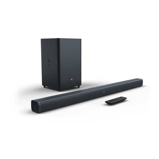
JBL BAR 2.1
2.1-Channel Soundbar with Wireless Subwoofer
SKU: JBLBAR21BLKAM, JBLBAR21BLKEP, JBLBAR21BLKUK, JBLBAR21BLKAS,
JBLBAR21BLKCN, JBLBAR21BLKBR
Released by Global Quality
CONTENTS
Technical Specifications
Safety Instruction, Warning & Notes
Software Upgrade Procedure
Troubleshooting Chart
Set Block Diagram
Schematic & Layout Diagrams
Set Mechanical Exploded View
Packaging Exploded View
Spare Parts List
Dismantling Instructions
Revision List
harman/kardon, Inc.
Service Manual
2
3
4
5
6
7
8
9
10
11
12
Ver. 1.4 Jul. 2018
Advertisement

Related Manuals for Harman JBL BAR 2.1


Summary of Contents for Harman JBL BAR 2.1
- Page 1 Service Manual JBL BAR 2.1 2.1-Channel Soundbar with Wireless Subwoofer SKU: JBLBAR21BLKAM, JBLBAR21BLKEP, JBLBAR21BLKUK, JBLBAR21BLKAS, JBLBAR21BLKCN, JBLBAR21BLKBR CONTENTS Technical Specifications Safety Instruction, Warning & Notes Software Upgrade Procedure Troubleshooting Chart Set Block Diagram Schematic & Layout Diagrams Set Mechanical Exploded View...
-
Page 2: Features And Benefits
® registered trademarks owned by Bluetooth SIG, Inc. and any use of such marks by HARMAN International Industries, Incorporated is under license. Other trademarks and trade names are those of their respective owners. The terms HDMI, the HDMI logo, and High-Definition Multimedia Interface are trademarks or registered trademarks of HDMI Licensing LLC in the United States and other countries. -
Page 3: Important Safety Instructions
Contact your local waste management officials for information NOTE: Changes or modifications not expressly approved regarding the environmentally sound collection, recycling and by Harman could void the user’s authority to operate the disposal of used batteries. equipment. To remove the batteries from your equipment or remote... - Page 4 Some semiconductor (solid state) devices can be damaged easily by static electricity. Such components commonly are called Electrostatically Sensitive (ES) Devices. Examples of typical ES devices are integrated circuits and some field effect transistors and semiconductor "chip" components. The following techniques should be used to help reduce the incidence of component damage caused by static electricity. 1.
-
Page 5: Ac Leakage Test
SAFETY PRECAUTIONS The following check should be performed for the continued protection of the customer and service technician. LEAKAGE CURRENT CHECK Measure leakage current to a known earth ground (water pipe, conduit, etc.) by connecting a leakage current tester between the earth ground and all exposed metal parts of the appliance (input/output terminals, screwheads, metal overlays, control shaft, etc.). -
Page 6: Software Upgrade Procedure
Software Upgrade Procedure 1. Put the "JBLBAR2_1.HUI" to the root directory of U disk, and step the U disk in Bar USB port. 2. Make sure your Bar connect with your Subwoofer by AUX cables. 3. Turn on your Bar and Subwoofer, make sure there are working. 4. Press down and hold the "Power" key and "Vol‐" key until the VFD show "Updata mode". 5. Wait a minute, it is updating when the vfd show "Wait". When it failed to upgrade VFDS will show "Fail". You need to check the step 1 and step 2. 6. The VFD will show that "Done" and reset when it update successfully. 7. You need to power off the Bar and Subwoofer, then power on they. -
Page 7: Keys Do Not Work
Keys do not work keysdonotwork Insteadofnew6pinline Check6pincable(XP6)tomainboardof connectyesornot.? ReplacetheoldwiththenewKEYboard Replacethekeyboard. totheEUTworking.yesornot? CheckfrommainboardtheSTB_3V3 CheckKEYsignalfromMCUmodule(U11) powersupplyisnormal?yesornot? inmainboard. Check the main board the MCU module ReplacetheMCUpartorotherloadparts parts( (U6)othersupplynetworkload for example:STB_3V3_MCU). ReplacePCBAformainboard.... - Page 8 BT cannot work BTcannotwork. Check the connection for BT antenna,yes or Replacetheantenna. not? CheckthepowersupplyoftheBT(BT_3V3). ReplacethePCBAformainboard. ReplacetheU21....
- Page 9 AUX IN cannot work AUX IN can not work Checkthe24pincable(XP7)tomainboardof Insteadofnew24pinline connectyesornot? ReplacetheoldwiththenewAUboardto ReplacetheAUboard. theEUTworking. CheckfrommainboardtheU14power ReplacetheU14. supplyisnormal?(SYS_5V_ADC、 SYS 3V3 ADC) ReplacePCBAformainboard....
- Page 10 HDMI ARC cannot work HDMI ARC can notwork Checkthe26pincable(XP9)tomainboardof Insteadofnew26pinline connectyesornot.? Replace the old with the new HD board to ReplacetheHDboard. theEUTworking. CheckfrommainboardtheU14isnormal? ReplacetheU14 (SYS_5V_ADC、SYS_3V3_ADC) ReplacePCBAformainboard....
- Page 11 OPTICAL cannot work OPTICAL can not work Checkthe24pincable(XP7)tomainboardof Insteadofnew24pinline connectyesornot.? Replace the old with the new AU board to ReplacetheAUboard. theEUTworking. CheckfrommainboardtheU14isnormal? ReplacetheU14 (SYS_5V_ADC、SYS_3V3_ADC) ReplacePCBAformainboard....
- Page 12 USB cannot work USBcannotwork Checkthe24pincable(XP7)tomainboardof Insteadofnew24pinline connectyesornot.? Replace the old with the new AU board to ReplacetheAUboard. theEUTworking. CheckfrommainboardtheU14isnormal? ReplacetheU14 (SYS_5V_ADC、SYS_3V3_ADC) ReplacePCBAformainboard....
- Page 13 SUB cannot work SUBcannotwork Check the TX is Normal (in the bar)? Yes or ReplacetheTXmodule. not? Check the White pair LED is Normal (in the Replace the RX module and 8pin SUB)?Yesornot? line. CheckfromAMboardtheU3isnormal? ReplacetheU3. (STB_3.3V) ReplacePCBAforAMboard....
- Page 14 Set Block Diagram X’tal X’tal FLASH SDRAM 27MHz 24.576MHz 74LVC244 I2C1/I/Os Downmix I2S HDMI CEC/HPD HDMI SUB I2S Syncomm Repeater 5.1CH I2S IA9Q5 CS497014 SiI9533 ARC SPDIF HDMI L Woofer 25W SUB I2C/I/Os Ω UART/I/Os Woofer FLASH 2.0 I2S I2S1 BT Module 12Ω...
- Page 15 Circuit Diagram:Power board and KEY board of subwoofer CX502 F501 0.33uF/275VAC BD501 LIF501 R509 R507 LF502 GBU4M FUSE_3.15A/250V CN501 T501 R504 C503 PQ32 C501 R510 R536 R502 R505 0.0022uF(222)400V 6.6MH C515 R508 C516 R531 R524 470pF/1KV 100V-240V RV501 30UH 270K 270K 270K 22nF...
- Page 16 Circuit Diagram:Power board Circuit Diagram:Power board and KEY board of subwoofer 8PIN/1.0mm STB_3V3 XP503 P_KEY Lk_LED TB_LED DATA STB_3V3 STB_3V3 NC/2K Q7 NC/PNP_3CG3906M JACK1 N/R70 NC/10K DATA NC/4.7K P_KEY Lk_LED NC/NPN_3DG3904M MP3 JACK <Description> TS-1307D WHITE_LED ORANGE_LED LED1 LED_ORANGE+WHITE...
- Page 17 Circuit Diagram:Power board of bar RS1M CON1_1 R29 62 FUSE_3.15AL/250V ATQ27 R28 62 KBP306 20mH 1000p 2200pF/630V 1000pF/630V 270K +24V1 2pin/7.92mm VDR/560V 1000p 0.33uF/275VAC 270K 100uF/400V 16*32mm 200uH min 20A/200V CON1_1 CON1_1 RS1M 470uF/35V 470uF/35V 4PIN/2.0mm/170mm 0.1uF/50V/X7R R7 4.7 VCC1 RS1M 270K BZX79B27...
- Page 18 Circuit Diagram:Amplifier board of subwoofer PVDD_34V STB_12V SY8292 10uH/2A 0.1uF/50V/X7R POWER INPUT SS26/60V/2A 300K/1% NC/56 100K 1uF/50V/X7R 100uF/50V PVDD_34V 15.4K/1% NC/330pF/50V/X7R 1000pF/50V/X7R 0.1uF/50V/X7R PW_LOW 7PIN/2.0mm SYS_12V STB_12V STB_3V3 SYS_3V3 P_AP2309 P_AP2305 PW_LOW 0.1uF/16V/X7R 0.1uF/25V/X7R STB_12V 100nF/25V X5R 0.1uF/25V 100K STB_3V3 100K 4.7uH/2.35A R142...
- Page 19 Circuit Diagram:Amplifier board Circuit Diagram:Amplifier board of subwoofer SYS_3V3 STB_3V3 STB_3V3 STB_3V3 R128 R129 8PIN/1.0mm R130 R131 Q6 NC/N_2SK3018 N_2SK3018 PAIR_KEY PAIR_KEY Link_LED AUX_DATA 5534_SDA Link_LED STB_LED STB_LED R132 AUX_CLK AUX_DATA NC/N_2SK3018 R140 NC/0 N_2SK3018 AUX_CLK 5534_SCL R133 R141 NC/0 SYS_3V3 R138 R139...
- Page 20 Circuit Diagram:Amplifier board Circuit Diagram:Amplifier board of subwoofer P_3V3 4700pF/50V/X7R 4700pF/50V/X7R P_3V3 1000/300mA SYS_3V3 TAS5534 PWM_HPM_L PWM_P_6 C39 C40 0.047uF/10V/X7R 0.047uF/10V/X7R PWM_HPP_L PWM_M_6 PWM_HPM_R PWM_P_5 PWM_HPP_R PWM_M_5 AVSS VR_PWM 0.1uF/16V/X7R PLL_FLTM AVSS_PWM PLL_FLTP AVDD_PWM SUB+ NC/4.7K 4.7K NC/10K VR_ANA PWM_P_8 SUB- NC/4.7K AVDD...
- Page 21 Circuit Diagram:Amplifier board Circuit Diagram:Amplifier board of subwoofer PVDD_34V SYS_12V 820uF/50V 0.1uF/50V/X7R 0.1uF/25V 10uF/25V C56 0.033uF/50V/X7R GVDD_AB BST_A C55 0.033uF/50V/X7R BST_B SUB- LAYOUT NOTE LAYOUT NOTE SUB- OC_ADJ SUB+ PLACE ON PLACE ON SUB+ VALID AMP_FAULT SPK JACK SIDE COMPONENT SIDE RESET AMP_FAULT 10uH/6.5A...
- Page 22 Circuit Diagram: Input board SYS_USB_5V1 10uF/10V/0805 0.1uF/16V/X7R USB JACK USB_DM USB_DM USB_DP C106 C107 NC/ACM2012H-900-2P U S B I N P U T 600/200mA DQR-012 STB_3V3 R110 OPTICAL_IN OPTI C102 DIGTAL_SENSE 24PIN/0.5mm STB_3V3 OPTICAL_IN SYS_USB_5V1 USB_DM USB_DP STB_3V3 LINE_IN_DET Audio_DET 0.1uF/16V/X7R AUX_R 0.1uF/16V/X7R...
- Page 23 Circuit Diagram:LED board STB_3V3_IR STB_3V3_IR SYS_5V_LED SYS_5V_LED R519 R517 R520 R518 LED_SCL_3V LED_SCL_5V LED_SDA_3V LED_SDA_5V N_2SK3018 N_2SK3018 ET6240 STB_3V3_IR COM4 SEG5 SEG4 COM3 SEG6 SEG3 SYS_5V_LED COM2 SEG7 SEG2 ROW0 DIG0 ROW1 COM1 DIG1 DIG1 SEG1 DIG1 ROW2 COM0 DIG2 DIG2 SEG0 DIG2...
- Page 24 Circuit Diagram:HDMI board RP1V STB_5V RP5V RP5V 855mA PNP_3CG3906M 2.2uH/3.4A STB_5V 0.1uF/16V/X7R R116 C137 STB_5V 1.8K 1.8K HD_PCON 68K/1% R117 HDMI_5V C138 2.2K TXD_SDA0 NC/EGA10402V05AH 2.2K TXD_SCL0 NC/EGA10402V05AH R118 0.1uF/16V/X7R TLV62565DBVR HD_PCON 4.7K 100K/1% NPN_3DG3904M R452 T0XC- ESD28 ESD29 NC/90/300mA TX0_HPD T0XC+ HDMI_5V...
- Page 25 Circuit Diagram:KEY board TS-1401 POWER_KEY POWER_KEY 600Ω 6PIN/1.25mm TS-1401 VOL-_KEY POWER_KEY KEY_V- KEY_SOURCE KEY_V+ 600Ω KEY_V- TS-1401 VOL+_KEY KEY_V+ 600Ω TS-1401 SOURCE_KEY KEY_SOURCE 600Ω C97 C98 C99 C100...
- Page 26 Circuit Diagram:Main board POWER_24V SYS_USB_5V1 10uH/2.5A POWER_24V VCC_AMP 100nF/25V/X5R CE14 0.1uF/16V/X7R 0.1uF/50V/X7R 150K/1% 100uF/16V/SMD 10uF/10V/0805 4PIN/2.0mm SYS_PCON 100u/35V TPS54202 20K/1% 100K 0.1uF/50V/X7R STB_5V STB_3V3 -5V_PWM 1uH/2.7A 100K 200K/1% C350 C351 POWER_24V MP1605 STB_5V 10uH/2.5A 100nF/25V/X5R 43.2K/1% 0.1uF/16V/X7R 100uF/16V/SMD 150K/1% 10uF/10V/0805 560K 100u/35V TPS54202...
- Page 27 Circuit Diagram:Main board AUX_L AUX_L AUX_R AUX_R C401 NC/10PF/50V C402 NC/10PF R401 NC/20K/1% R402 NC/20K/1% VCC_OP VCC_OP NC/4.7uF/10V/X5R AL_CH0 R324 2.7K/1% AUX_L U400A U400B NC/4.7uF/10V/X5R C405 C400 R400 20K/1% R403 NC/20K/1% OUT1 AL_CH0 OUT2 AR_CH0 R404 20K/1% R405 NC/20K/1% AR_CH0 AUX_R C404 4.7uF/10V/X5R...
- Page 28 Circuit Diagram:Main board AUX_L MUX_IN_L- 4.7uF/10V/X5R 20K/1% 24K/1% AUX_IN_L- 150pF/50V/NP0 4.7K/1% NJM4565M 1000pF/50V/X7R AVDD1 SYS_12V AVDD1 100K 100nF 10uF/16V/X5R 100K 10uF/16V/X5R 1UF/16V/X7R NJM4565M AVDD2 SYS_12V NC/200pF/50V/NP0 MUX_IN_L- 20K/1% 20K/1% MUX_IN_L+ AUX_IN_L+ 100nF 10uF/16V/X5R AUX_R 4.7uF/10V/X5R 20K/1% 24K/1% MUX_IN_R- AUX_IN_R- 150pF/50V/NP0 4.7K/1% 1000pF/50V/X7R NJM4565M...
- Page 29 Circuit Diagram:Main board STB_1V2 VDD12 R315 A_1V2 0.1uF/16V/X7R 10uF/6.3V 0402 SYS_3V3 PLL_VDD12 10uF/6.3V 0402 0.1uF/16V/X7R HD_MUTE 4 HD_INT D_3V3 STB_3V3 HD_RST LED_SDA R316 LED_SCL Audio_DET 4 R319 0.1uF/16V/X7R VDD33_USB 10uF/6.3V 0402 500/200mA 0.1uF/16V/X7R 10uF/6.3V 0402 VDD33_ADAC D_3V3 CS42528_RST WL_BUSY UART2_RTS/GPIO30 AOUT_R/GPIO138 A_VREF WL_SCL...
- Page 30 Circuit Diagram:Main board 47pF/50V/NP0 DV+3.3V 47pF/50V/NP0 47pF/50V/NP0 FB5 160 CS_DATA CS_LRCLK CS_SCLK 0.1uF/16V/X7R 4.7UF/6.3V/X5R DV+5V DIR_RMCLK FB6 500/200mA DIR_OMCLK DSP_I2S0_DATA1 DSP_I2S0_DATA0 0.1uF/16V/X7R 4.7UF/6.3V/X5R DSP_I2S0_SCLK DSP_I2S0_LRCLK DV+5V 10pF/50V/NP0 500/200mA 10uF/10V/0805 0.1uF/16V/X7R DV+3.3V 500Ω CX_SDIN1 RXP1/GPO1 0.1uF/16V/X7R BT_SPDIF CX_SCLK RXP2/GPO2 0.1uF/16V/X7R DV+3.3V OPT_SPDIF CX_LRCK RXP3/GPO3...
- Page 31 Circuit Diagram:Main board DV33 DSP_RESET DSP_RST DSP_INT DSP_INT DSP_BSY R108 R109 R110 R111 R112 DSP_BUSY CS_LRCLK CS_LRCLK CS_SCLK 8PIN/0.5mm DSP CS497014 CS_SCLK CS_DATA CS_DATA DSP__CLK_SW R113 GPIO35, SCP1_CLK EXT_A19 DSP_MOSI_SW R115 GPIO33, SCP1_MOSI EXT_A18 TO MCU SPI_MISO_SW R116 GPIO34, SCP1__MISO / SDA EXT_A17 DSP_CS_SW SD_3V3...
- Page 32 Circuit Diagram:Main board SYS_3V3 C194 C195 SYS_5V 26PIN/1.27mm FB12 NC/600/1A SYS_3V3 10UF/6.3V/X5R C156 STB_3V3 FB17 600/1A 100nF R177 NC/10uF/6.3V/X5R C172 NC/100pF/50V/NP0 C200 NC/100pF/50V/NP0 C150 C143 NC/100pF/50V/NP0 NC/0.1uF/16V/X7R 6PIN/1.25mm C144 NC/100pF/50V/NP0 R139 NC/33 SYS_3V3 IA9Q_SCL_ R141 NC/33 W_BUSY IA9Q_SDA WL_BUSY 3 R185 POWER_KEY KEY_POWER...
- Page 33 Circuit Diagram:Main board FB22 300/3A VCC_AMP C239 GVDD0 C240 0.1uF/50V/X7R 220uF/35V 1000pF/50V/X7R C241 1UF/16V/X7R R236 R233 INPR_WF AMP_INP_R_WF AGND 100K C242 WF OUT+ R235 100pF/50V/NP0 R234 C243 10uH/4.5A R237 NC/0 MODSEL PVCC C244 R238 R239 FR_WF+ 100pF/50V/NP0 C245 100pF/50V/NP0 NC/22 /SDZ PVCC 1UF/16V/X7R...
- Page 34 Circuit Diagram:Main board 300/3A FB23 VCC_AMP C276 C277 C278 C275 GVDD2 CE10 0.1uF/50V/X7R 1000pF/50V/X7R 220uF/35V C279 1UF/16V/X7R R257 AMP_INP_L_WF INPL_WF R256 R258 AGND R259 NC/0 FL_WF+ C280 WF OUT+ 100K R285 100pF/50V/NP0 10uH/4.5A R260 AGND MODSEL PVCC C281 R261 R262 /SDZ_L 100pF/50V/NP0 NC/22...
- Page 35 7-21 PCB Layout:Power board and KEY board of subwoofer...
- Page 36 7-22 PCB Layout:Power board of bar...
- Page 37 7-23 PCB Layout:Amplifier board of subwoofer(bottom)
- Page 38 7-24 PCB Layout:Amplifier board of subwoofer(top)
- Page 39 7-25 PCB Layout:Input board...
- Page 40 7-26 PCB Layout:LED board...
- Page 41 7-27 PCB Layout:HDMI board(BOTTOM VIEW)
- Page 42 7-28 PCB Layout:HDMI board(TOP VIEW)
- Page 43 7-29 PCB Layout:KEY board of bar...
- Page 44 7-30 PCB Layout:Main board...
- Page 45 MECHANICAL EXPLODED VIEW OF MAIN UNIT 1+2+3+30 08-SB21GS-000 GRILLE ASS'Y W/LOGO,BUTTON BRACKET BAR2.1 6+7+11+13+1 5+17+28+21+ 42-031020-12001 MID-RANGE SPEAKER 44x74mm BAR2.1&3.1 07-WLIA9Q-5S8 WIRELESS MODULE IA9Q5 BAR2.1&3.1 02-SB3121-XX0 SCREW FOR WALL MOUNT BAR2.1&3.1 & &...
- Page 46 MECHANICAL EXPLODED VIEW OF SUBWOOFER Pos. No. Part Number Description Usage SUB4 42-065100-04001 6.5" WOOFER BAR2.1 SUBWOOFER SUB6 56-SB20E1-0HAB1 FOOT BRACKET BAR2.1 SUBWOOFER SUB7 59-223530-000B1 RUBBER FOOT BAR2.1 SUBWOOFER SUB10 08-SB210U-KE0 KEY BOARD BAR2.1 SUBWOOFER SUB11+22 02-SB21K1-XX0B1 BUTTON ASSY BAR2.1 SUBWOOFER SUB15 08-SB210U-AC0 POWER SOCKET BAR2.1 SUBWOOFER...
- Page 47 PACKAGING EXPLODED VIEW BAR EPE TRAY Bar bag Accessories box Gift box Packing bar Accessories box Bar card Subwoofer EPE tray Packing tape Subwoofer bag Packing subwoofer Paper card Carton box...
- Page 48 JBL BAR 2.1 SPARE PARTS LIST V1.3 Pos. No. Part Number Description Usage 1+2+3+30 08-SB21GS-000 GRILLE ASS'Y W/LOGO,BUTTON BRACKET BAR2.1 55-SB21F2-0UA MIDDLE FRONT COVER BAR2.1 08-SB210U-AU0 INPUT BOARD BAR2.1 67-SB21V0-0E0 SHIELD SHEET BAR2.1 08-SB210U-HD0 HDMI BOARD BAR2.1 55-SB21L0-0HAB1 LEFT SIDE COVER BAR2.1 08-WLIA9Q-TX0 WIRELESS MODULE IA9Q5 SB2.1...
- Page 49 46-NN010T-08SF CABLE 8P/1.25mm/100mm 300V BAR2.1 46-NN014T-06SF CABLE 6P/140mm/1.25mm 300V BAR2.1 47-ANT317-XX0 BT ANTENNA 2.4G 1.13mm BAR2.1 46-KK012C-08AVF FFC 8P/1.0mm/120mm BAR2.1 SUBWOOFER 46-KL018T-02J SPK WIRE 2P #22 BAR2.1 SUBWOOFER 76-SB21G0-0ATB8 GIFT BOX BAR2.1 JAPAN VERSION 51-R70150-0RR01-A POWER CORD JET 1.5M BAR2.1 JP 74-103023-60HB2 POLY BAG FOR MAIN UNIT BAR2.1 76-SB21G0-0ATB3...
- Page 50 DISMANTLING INSTRUCTIONGS 1. Remove 12 screws ,then carefully separate the right cover and left cover by a tweezer ,then take out the iron net cover. 2.Remove 2 screws on the KEY board ,then take out the board 3.Remove 8 screws on the middle cover ,then take out the cover 4.Pull off 3 FFC cable and remover the screw on top side of the main board ,then remove 2 screws and pull off the FFC cable on the LED board ,the take out LED board.Pull off 3 FFC cables on the back side of main board ,the get the board.
- Page 51 5.Remove 3 screws on HDMI board , take out the board. 6.Remove 3 screws on power board ,then get the board. Remove 2 screws and disconnect the FFC cable on input board ,then get the board.
-
Page 52: Revision List
REVISION LIST Version 1.0 *Initial release for JBL Bar 2.1 2017-07 Version 1.1 * Delete JBL Bar 3.1 BT module from JBL Bar 2.1 spare parts list 2017-08 Version 1.2 * WIFI MODULE P/N updated on page 48. 2017-12 Version 1.3 *Add UK Power Cord in parts list.
Need help?
Do you have a question about the JBL BAR 2.1 and is the answer not in the manual?
Questions and answers