Table of Contents
Advertisement
Quick Links
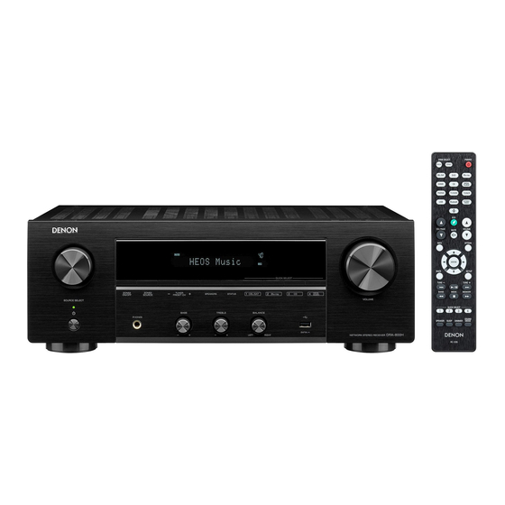
NETWORK STEREO RECEIVER
DRA-800H
• For purposes of improvement, specifications and design are subject to change without notice.
• Please use this service manual when referring to the operating instructions without fail.
• Some illustrations used in this service manual are slightly different from the actual product.
Service Manual
Click here!
On-line service parts list
http://dmedia.soundunited.com/documents/details/25798
s
ONLINE PARTS LIST
(P5)
WEB owner's manual
NA:
http://manuals.denon.com/DRA800H/NA/EN/index.php
EU:
http://manuals.denon.com/DRA800H/EU/EN/index.php
Upload is planned for the time of a future press release.
BEFORE SERVICING THIS UNIT
ELECTRICAL
MECHANICAL
REPAIR INFORMATION
UPDATING
Please refer to the MODIFICATION NOTICE.
Confidential
Ver. 2
Advertisement
Table of Contents

Related Manuals for Denon DRA-800H


Summary of Contents for Denon DRA-800H
- Page 1 Service Manual Ver. 2 NETWORK STEREO RECEIVER DRA-800H Click here! On-line service parts list http://dmedia.soundunited.com/documents/details/25798 ONLINE PARTS LIST (P5) WEB owner’s manual http://manuals.denon.com/DRA800H/NA/EN/index.php http://manuals.denon.com/DRA800H/EU/EN/index.php Upload is planned for the time of a future press release. BEFORE SERVICING THIS UNIT ELECTRICAL...
- Page 2 BEFORE SERVICING THIS UNIT SAFETY PRECAUTIONS NOTE FOR SCHEMATIC DIAGRAM HANDLING THE SEMICONDUCTOR AND OPTICS ONLINE PARTS LIST Accessing the Parts List Searching Part Numbers or Ref. Numbers NOTE FOR PARTS LIST SERIAL NUMBER Serial Number Organization SKU Code of this Unit POST-SERVICE PRECAUTIONS Initializing this Unit...
-
Page 3: Safety Precautions
SAFETY PRECAUTIONS The following items should be checked for continued protection of the customer and the service technician. Leakage current check Before returning the set to the customer, be sure to carry out either (1) a leakage current check or (2) a line to chassis resistance check. If the leakage current exceeds 0.5 milliamps, or if the resistance from chassis to either side of the power cord is less than 460 kohms, the set is defective. -
Page 4: Note For Schematic Diagram
NOTE FOR SCHEMATIC DIAGRAM WARNING: Parts indicated by the z mark have critical characteristics. Use ONLY replacement parts recommended by the manufacturer. CAUTION: Before returning the set to the customer, be sure to carry out either (1) a leakage current check or (2) a line to chassis resistance check. -
Page 5: Note For Parts List
Click here! On-line service parts list http://dmedia.dmglobal.com/Document/DocumentDetails/XXXXX ONLINE PARTS LIST (P5) WEB owner’s manual http://manuals.denon.com/AAAAAAA/NA/EN/index.php http://manuals.denon.com/AAAAAAA/EU/EN/index.php http://manuals.denon.com/AAAAAAA/AP/ZH/index.php http://manuals.denon.com/AAAAAAA/JP/JA/index.php Upload is planned for the time of a future press release. BEFORE SERVICING THIS UNIT NOTE : If the web browser does not open automatically, copy the URL and paste it into the address bar (3) Next, click the "Sheet"... - Page 6 SERIAL NUMBER Serial Number Organization The 14-digit serial number that contains the code of the manufacturing plant and the manufacturing date. 14 digits Factory Manufactured Cumulative Year, month code code serial number The last Month 2digit of year (01 ~ 12) SKU Code of this Unit Product SKU SKU Code...
-
Page 7: Initializing This Unit
POST-SERVICE PRECAUTIONS Initializing this Unit Make sure to initialize this unit after replacing the microcomputer or any peripheral equipment, or the digital PCB. 1. Press the power button to turn off the power. 2. While holding down buttons "TUNER PRESET CH -" and "SPEAKER" simultaneously, press the power button to turn on the power. -
Page 8: Schematic Diagrams
ELECTRICAL SCHEMATIC DIAGRAMS PRINTED CIRCUIT BOARDS SCH01 HDMI RX DIGITAL, TUNER(E3), PHONO, DAB(E2) SCH02 HDMI TX MAIN, PHONE WIRE GUIDE, USB CABLE GUIDE SCH03 OSD SMPS, FRONT, PHONE, FUNCTION VR, USB SCH04 DIGITAL SUPPLY SCH05 MCU LEVEL DIAGRAM SCH06 MCU LEVEL CHG FRONT ch SCH07 DIR SUBWOOFER ch... - Page 9 SCHEMATIC DIAGRAMS SCH01 HDMI RX HDMI_RX PART TO 0A TO OSD PART CEC3V3 CEC1V1 DGND AVDD33RX AVDD33RX L7102 TO 1A CLZBLM21PG300SN1D VDD33 VDD33 L7103 CB05YTYH221 PVDD33 PVDD33 L7104 CB05YTYH221 AVDD33TX AVDD33TX L7105 CB05YTYH221 VDD33IO VDD33IO L7106 CB05YTYH221 Q7101 HVTKRC102S Q7102 JK701 HVTKRC102S R7134...
- Page 10 SCH02 HDMI TX HDMI_TX PART CEC5V CEC3V3 L7201 VDD33_TX VDD33_TX CEC1V1 CB05YTYH221 DGND TX2+ PVDD33_TX PVDD33_TX L7202 TX2- CB05YTYH221 TX1+ TX1- TO 7A TX0+ AVDD33RX_TX AVDD33RX3_TX L7203 TX0- OPEN AVDD33RX2_TX TXC+ L7209 TO 5A TXC- CB05YTYH221 AVDD33RX1_TX AVDD33RX0_TX AVDD33TX_TX L7204 AVDD33TX_TX CB05YTYH221 TX0_CM...
- Page 11 SCH03 OSD OSD PART OSD_SPI_MO OSD_SPI_MI OSD_SPI_CS OSD_SPI_CLK NET3.3V GUI_WRITE TO 2B Q7301 HVTKRC102S +1V8H2 ADV7623_RST HSCL HSDA X7301 ADV7623_SPI_MI 28.6363MHz ADV7623_SPI_MO R7362 R7329 C7331 ADV7623_SPI_CLK C7338 10/6.3V OPEN ADV7623_SPI_CS C7330 7623_ROM_HOLD 500 ohm OPEN OPEN C7340 TO 3B C7341 OPEN <DVDDIO_3V3>...
-
Page 12: Digital Supply Part
SCH04 DIGITAL SUPPLY DIGITAL SUPPLY PART CN741 CN741 CJP06GA01ZY L7401 1.D5.2V CB03YTYH600 L7402 2.D5.2V TO BN601 R7483 CB03YTYH600 3.M_RESET L7403 CB03YTYH600 4.DGND 5.DGND D3.3V R7451 R7453 L7404 6.MAIN_POWER CB03YTYH600 L7414 NET5V_POWER R7410 Q7401 D5V_POWER R7411 L7415 HVTKRC104S D5V_POWER OPEN OPEN D5V_POWER IC741 L7411... - Page 13 AVCC0 CEC_OUT C7517 0.1uF R7514 E_TXD_MOEI DSP_MOSI DSP_MOSI TXD0 DSP_MISO DSP_MISO DSP_CLK DSP_CLK TO 4C DSP_RST DSP_RST DSP_FLAG0 DSP_FLAG0 * DRA-800H VERSION OPTION VER. R7581(PU) R7582(PD) R7505 DRA-800HE3 OPEN 3.3k R7508 DRA-800HE2 OPEN X7501 DAC_RST DAC_RST DAC_DATA DAC_DATA 12.0MHz ET751...
- Page 14 SCH06 MCU LEVEL CHG CN753 TO BN502 TO MAIN B'D MCU_LEVEL_CHG PART 2.0mm 11PIN WAFER CN756 CN753 CJP03GI288ZY CJP11GI288ZY C7594 0.047uF FROM SWM3.3V DIGITAL DGND SUPPLY TO C0 CN755 CJP04GB113ZY 1.3.3V 2.TX 3.RX 4.DGND R7589 R7592 Q7593 HVTKRC102S TO C1 FROM/TO MCU PART GND LINE...
- Page 15 SCH07 DIR FROM MCU PART TO C7 DIR PART (2) DIR output CH1:DIRLRCK (FSDIR1) SPDIF_OUT HDMISPDIF DIRMCK CH2:DIRBCK DIRBCK (64FSDIR1) DIRLRCK DIRDATA MPIO_B3 MPIO_B2 CH3:DIRDATA MPIO_B1 (DATADIR1) MPIO_B0 DIRAUXDATA DR_CE 256FSDIR1 DIRAUXLRCK DIRAUXBCK DR_CK 64FSDIR1 DIRAUXMCK DR_DIN FSDIR1 DIRXMCK DR_DOUT DATADIR1 DIRSLRCK DIRSBCK...
- Page 16 SCH08 PLD TO C6 TO 5D PLD PART FROM MCU PART FROM LEGO PART JTAG_TMS JTAG_TDI JTAG_TCK R7748 TDO1_TDI2 SPDIF_OUT SPDIF_OUT MCLK_I2S_0 PLDERR MCLK_I2S_0 LRCK_I2S_0 LRCK_I2S_0 AP_CS SDIN_I2S_0 SDIN_I2S_0 AP_DA SCLK_I2S_0 SCLK_I2S_0 AP_CK SDOUT_I2S_0 SDOUT_I2S_0 LRCK_I2S_1 APLD_CS LRCK_I2S_1 SDIN_I2S_1 APLD_DATA SDIN_I2S_1 SCLK_I2S_1 APLD_CLK...
- Page 17 SCH09 DSP DSP PART TO C9 TO D4 FROM PLD PART FROM DIR PART FROM L7801 CB03YTYH600 DA1.1V DIGITAL SUPPLY L7802 CB03YTYH600 DA3V3 PART DGND DO_S TO B8 DO_F DO_C DI_-/SW DI_S/SL DI_BCK DI_-/FR DI_MCK DI_CSW/C DI_LRCK DO_BCK DO_LRCK DI_F/FL DI_SB/SR R7822 D_FLG0...
-
Page 18: Main Dac Part
SCH10 MAIN DAC MAIN DAC PART TO D3 FROM PLD PART C7985 0.047uF C7986 0.047uF C7987 1000pF C7988 1000pF C7989 OPEN C7990 OPEN C7991 1000pF C7992 1000pF C7993 1000pF C7994 0.047uF R7916 C7995 0.047uF R7917 C7996 0.047uF 4k7/F-T DA_Z_MUTE1 C7997 1000pF R7911 C7913... -
Page 19: Pin Connector
SCH11 NETWORK FROM LEGO M ODULE I2S_0 LEGO OUTPUT I2S_1 BT_TX I2S_2 LEGO INPUT(Zone2) 42 Pin CONNECTOR 80 Pin CONNECTOR CN811 CN812 CJP80GA370ZU CJP42GA370ZU LEGO5V BK811 BK812 BK813 BK814 DGND VMD1A960 VMD1A960 VMD1A960 VMD1A960 NET3.3V SWM3.3V C8107 OPEN VOUT_D22 VOUT_D23 TO B6 VOUT_D20 IC811... -
Page 20: Analog Part
SCH12 ALALOG ANALOG PART CN821 * TUNER/DAB OPTION PHONO-L REF NO C8283/C8284 C8289/C8290 C8285/C8286 R8223/R8224 R8225/R8226 R8227/R8228 R8236/R8237 R8238/R8239 R8293/R8294/R8295 AGND E3 VERSION 220p OPEN 50V/10uF 100k OPEN OPEN PHONO-R E2 VERSION 100p 100p OPEN 3.6k OPEN 3.6k +7.5V -7.5V CH_GND E2 VERSION CH_GND... - Page 21 RLY_GND CJP07GA90ZY OPEN FUSE OPTION Q5705 Q5708 2SC3052 2SC3052 MODEL F3001 F3002 F3003 F3004 AC120V OPEN OPEN 932Series 932Series DRA-800H Q5703 Q5704 Q5706 Q5707 2SC3052 ISA1530AC1 2SC3052 ISA1530AC1 AC230V 218Series 218Series OPEN OPEN DC PROTECTION B+/B- POWER DETECT BN502 BN502...
- Page 22 FOR CORSSTALK NOISE(PREPAIR) BN826_ 1.L-OUT 2.R-OUT 3.VCC 4.SCLK 5.SDIO 6./CE 7./RST 8.INT 9.CH_GND BN826 TO BN826-1 TUNER B'D (CUP12959Z-2) *TUNER / DAB MODULE OPTION DRA-800H E3 CNVYST990-A9U2 DRA-800H E2 NO USED TU800 BN826-1 BN826-1 CH_GND 9.CH_GND 8.INT 8.INT 7./RST 7./RST 6./CE 6./CE 5.SDIO...
-
Page 23: Front Part
SCH15 FRONT BN12B1 TO CN751 FROM DIGITAL B'D 1.25mm 27PIN FFC FRONT PART FL101 1.25-2S-27PW BN12B1 CFL18BT021GINK RC101 38KHZ CUP13026Z-2 F1001 BK101 BK102 PCB BRAKET (38kHz) T 200mA L 250V D1001 OPTION "A" 1N4007SL Q1001 BN103A/BN103B J1001 - J1006 KTC1027YT CMD1A572 CMD1A572 OPTION... - Page 24 SCH16 DAB DAB B'D L8301 IC831 DA+5V DAB3.3V CB03Y T Y H 600 AP7361-Y -13 26. SPI_CS 25. GND 24. SPI_TXD 23. SPI CLK CN861 22. GPIO 21. GPIO 9.GND 20. GPIO R8314 R8316 19. GPIO 8.SIG_GND R8309 18.UART RXD R8313 R8310 7.DAB_EN...
- Page 25 SCH17 SMPS SMPS PART OPTION *OPTION AC100~ 120V T 2A L 250V C6002 250V/0.01uF *OPTION *OPTION AC220~ 230V T 1.6A L 250V F6001 D 6001 1N4007 D 6002 1N4007 D 6003 1N4007 D 6004 1N4007 LF602 D 6005 1N4007 E3,K:LF-4ZB-E273H E2,E1C:LF-4ZB-E503H D 6006 1N4007 R6034...
- Page 26 PRINTED CIRCUIT BOARDS DIGITAL, TUNER(E3), PHONO, DAB(E2) Lead-free Solder When soldering, use the Lead-free Solder (Sn-Ag-Cu). DIGITAL (A SIDE) DRA-800H DIGITAL MP_CUP13029Z_A CN821 CK_5 DA_3 CK_3 DA_1 CK_1 DA_OUT CK_OUT DA_5 DA_4 CK_4 1.TUNER-L 2.TUNER-R 3.VCC 4.TUNER_SCLK 5.TUNER_SDIO 6.TUNER_CE JK751 +5V_OUT 7.TUNER_RST...
- Page 27 MAIN, PHONE WIRE GUIDE, USB CABLE GUIDE MAIN (A SIDE) MAIN (B SIDE) PHONE WIRE GUIDE (A SIDE) CUP13027-3 Z MP USB CABLE GUIDE (A SIDE) CUP13027-2 Z MP...
- Page 28 SMPS, FRONT, PHONE, FUNCTION VR, USB FRONT (A SIDE) FRONT (B SIDE) SMPS (A SIDE) SMPS (B SIDE) 1.ISEL_A 2.ISEL_B 3.BAL_A 4.POWER_KEY 5.BAL_B 6.BAS_A C1073 7.BAS_B C1074 8.TRE_A 9.TRE_B D1015 10.H/P_DET D1016 11.VSEL_A 12.VSEL_B 13.KEY_3 14.KEY_2 15.KEY_1 16.RED_LED 17.GRN_LED 18.RC_IN 19.FL_RST 20.FL_CE 21.FL_CLK...
-
Page 29: Level Diagram
LEVEL DIAGRAM FRONT ch... - Page 30 SUBWOOFER ch...
- Page 31 ZONE2 ch...
-
Page 32: Block Diagram
BLOCK DIAGRAM ANALOG AUDIO DIAGRAM DRA-800H ANALOG AUDIO BLOCK VOLUME IC V+ :+ 7.5V V-:-7.5V NJU72343V VCC:D AB+ 3.3V * LOGIC CONTROL H IGH LEVEL INPUT VOLTAGE(MIN: + 2.5V / MAX: V+ ) P-AMP SELECT IC SPK OUT SPEAKER A RELAY... - Page 33 TXAVDD:+1V8H TXPVDD:+ 1V8H TXPLVDD:+ 1V8H DVDDIO:DV3V3 TVDD:DV3V3 OUT0 TMDS P0TX TMDS HDMI IN4 (GAME) OUT1 TMDS P1TX * DRA-800H: NO USED SIGNAL TMDS HDMI IN5 (MEDIA Player) VDD11: CEC1V1 VDD33:CEC3V3 AVDD11:CEC1V1 AVDD33:CEC3V3 AVDDH33:CEC3V3 PVDD33:CEC3V3 DSP_MOSI DSP_MISO ADSP21487KSW Z-2B DSP_CLK DSP_RST...
- Page 34 VIDEO DIAGRAM DRA-800H VIDEO BLOCK CVDD, DVDD:+ 1V8H PVDD:+ 1V8H TXAVDD:+1V8H TXPVDD:+ 1V8H TXPLVDD:+ 1V8H DVDDIO:DV3V3 TVDD:DV3V3 AD V7623 HDMI RX(MN864787) TRANSCEIVER 28.6363MH z OSD Block P2 RX HDMI IN1 (CBL/SAT) TXPORT0 P1 RX HDMI IN2 (DVD) S.FLASH P0 RX...
-
Page 35: Power Diagram
POWER DIAGRAM DRA-800H VCC DIAGRAM HI+ B MAIN+ B LOW+ B MAIN-B S1(AMP+ B,-B) H I-B 57m A SELETOR IC,VOLUME IC LOW -B (NJU72750AV,NJU72343V,NJM2068) MM1Z7V5 196m A A+ 12V (NJM8080,SPK/H-P/HI-LOW RELAY) 102m A BU33TD3WG DA+ 3.3V (AK4458VN,PCM5100A) KIA7812BPI 81m A... -
Page 36: Wiring Diagram
WIRING DIAGRAM DRA-800H W IRING DIAGRAM AC CORD ANT1 ANT2 PCB TO PCB DIGITAL PCB CN821 TUNER CN862 REGUL.-> DIGITAL MOD ULE CN825 BN826 (CUP13029Z) TUNER PCB (E3) CN813 CN861 (CUP12959Z-2) SMPS-> DIGITAL LEGO CN741 DAB PCB (E2) (CUP13026Z) CN826... - Page 37 SEMICONDUCTORS Only major semiconductors are shown, general semiconductors etc. are omitted to list. The semiconductor which described a detailed drawing in a schematic diagram are omitted to list. 1. IC's R5F5651EDDFB (DIGITAL_MCU : IC751) Pin Name Symbol Pu/Pd STBY STOP CEC Function STBY 24 UPSEL/P35(IN)/NMI DSP_FLAG0...
- Page 38 Pin Name Symbol Pu/Pd STBY STOP CEC Function Pin Name Symbol Pu/Pd STBY STOP CEC Function STBY STBY 57 VSS Ground pin 104 P70 Hi-B_RL HIGH-B relay control pin 58 P83 TRE_A SW3VPu Tone TREBLE (Rotary encoder) signal input pin 105 VSS Ground pin 59 VCC...
- Page 39 ADV7623 (DIGITAL_OSD : IC731) Pin Name Symbol Pu/Pd STBY STOP CEC Function STBY 143 AVCC0 AVCC0 Power supply pin 144 P07/IRQ15 CEC_OUT CEC-D control pin DDCC_SCL DDCA_SDA CVDD PIN 1 RTERM CGND 5V_DETA RXC_C– HP_CTRLA RXC_C+ PGND TVDD PVDD RXC_0– XTAL1 RXC_0+ XTAL...
- Page 40 Pin No. Mnemonic Type Description Pin No. Mnemonic Type Description RXC_2− HDMI input Digital Input Channel 2 Complement of Port C in the HDMI Interface. RXC_2− HDMI input Digital Input Channel 2 Complement of Port C in the HDMI Interface. RXC_2+ HDMI input Digital Input Channel 2 True of Port C in the HDMI Interface.
- Page 41 ADV7623 Block diagram Pin No. Mnemonic Type Description PGND Ground PVDD Ground. PVDD Power PLL Supply Voltage (1.8 V). XTAL Miscellaneous Input pin for 28.63636 MHz crystal or an external 1.8 V 28.63636 MHz clock oscillator source to XTAL XTAL1 analog clock the ADV7623.
- Page 42 DIGITAL_OSD : IC732 TPS563201 (DIGITAL_DIGITAL SUPPLY : IC741, IC742, IC743, IC744) BY25Q32BSSIG (except : E2) DDC Package 6-Pin SOT BY25Q64ASSIG (only E2) Top View VBST Top View Pin Name Description Chip Select Serial Output for single bit data Instructions. IO1 for Dual or Quad SO (IO1) Instructions.
- Page 43 MC74HC4094ADR2G (DIGITAL_MCU : IC752, IC753) SN74LVC244APWR (DIGITAL_OSD : IC734) (DIGITAL_PLD : IC772) SRG8 (DIGITAL_DSP : IC783) (DIGITAL_LEGO : IC812) (DIGITAL_HDMI_TX : IC722) MC74HC4094A Logic Diagram SN74LVC244A Figure 1. Pin Assignment OCTAL BUFFER/DRIVER WITH 3-STATE OUTPUTS www.ti.com STAGE 0 STAGES 1 TO 6 STAGE 7 SCAS414X –...
- Page 44 www.ti.com SBAS495 – JUNE 2010 PIN CONFIGURATIONS PT PACKAGE PCM9211PTR (DIGITAL_DIR : IC761) LQFP-48 (TOP VIEW) DESCRIPTION NAME TOLERANT DVDD – – Power supply, 3.3 V (typ.), for digital Software control I/F, SPI data output / I2C slave address set- MDO/ADR0 ting0(2) ERROR/INT0...
- Page 45 www.ti.com SBAS495 – JUNE 2010 BLOCK DIAGRAM ADSP21487KSWZ2B (DIGITAL_DSP : IC781) PCM9211PTR BLOCK DIAGRAM FILT AUXIN 0 AUTO RXIN7 RXIN 0 RXIN0 SCKO DOUT RXIN 1 RXIN1 MAIN OUTPUT PIN 1 RXIN 2 RXIN2 AUXIN0 LRCK SCKO/ BCK/LRCK PORT AUXIN1 DOUT RXIN 3 RXIN3...
-
Page 46: Pin Configuration
BY25D16ASSIG (DIGITAL_DSP : IC782) A3V64S40GTP-60 (DIGITAL_DSP : IC784) PIN CONFIGURATION (TOP VIEW) Top View DQ15 VddQ VssQ SOP8 150/208mil DQ14 SCLK DQ13 VssQ VddQ DQ12 DQ11 VddQ VssQ DQ10 Terminal Functions VssQ VddQ Pin Name Description LDQM UDQM Chip Select /CAS /RAS SO (IO1) - Page 47 AK4458VN 40 +105 C (Exposed pad is connected to ground) 40 +85 C (Exposed pad is open) 48-pin QFN (0.5mm pitch) AKD4458 Evaluation Board for AK4458 AK4458VN (DIGITAL_MAIN DAC : IC791) No. Pin Name I/O Function PD State CAD0_I2C Chip Address 0 Pin in I2C Bus serial control mode Pin Configurations Chip Select Pin in 3-wire serial control mode Hi-Z...
-
Page 48: Functional Block Diagram
[AK4458] FUNCTIONAL BLOCK DIAGRAM BD82065FVJ-E2 (DIGITAL_NETWORK : IC814) 4. Block Diagram and Functions LDOE TVDD VDD18 DVSS AVDD AVSS Bias BICK/DCLK DATT AOUTL1P LRCK/DSDL1 Soft Mute Interpolator AOUTL1N SDTI1/DSDR1 Data SDTI2/DSDL2 Interface VREFH1 Vref De-empha SDTI3/DSDR2/TDMO1 DATT Modulator VREFL1 DSD Filter Soft Mute SDTI4/DSDL3/TDMO2 Noise... - Page 49 NJU72343 (DIGITAL_ANALOG : IC822) NJM41050V (DIGITAL_ANALOG : IC881) VIN1 75 DRV 0.1µF CLAMP 6.75MHz 47µF 75 VOUT VIN2 VSAG 0.1µF CLAMP 1µF No. Symbol Function No. Symbol Function SREFV VIN3 AREF Analog reference potential DATA IC control data input Address selection CLOCK IC control clock input 0.1µF...
- Page 50 TOP268VG (SMPS : IC601) AK5358BET(DIGITAL_DIR : IC764) DRAIN (D) CONTROL (C) INTERNAL SUPPLY SHUNT REGULATOR/ ERROR AMPLIFIER SOFT START 5.8 V 4.8 V INTERNAL UV 5.8 V PS(UPPER) COMPARATOR V I (LIMIT) CURRENT LIMIT ADJUST ÷ 16 PS(LOWER) ON/OFF SHUTDOWN/ EXTERNAL CURRENT AUTO-RESTART CURRENT LIMIT...
-
Page 51: Pin Connection
2. FL DISPLAY FLD (018BT021GINK) (FRONT : FL101) ANODE CONNECTION 17G(AD3) 18G(AD4) 8G 9G 10G 11G 12G 13G 14G 15G 16G PIN CONNECTION NOTE 1) F1, F2 ----Filament 2) NP ------No pin 3) DL ------Datum Line 4) NX ------No extend pin 5) LGND ----Logic GND pin 6) PGND ----Power GND pin 7) VH... - Page 52 3. Remote Code Table FORMAT SHARP FORMAT: SHARP /DATA CONSTRUCTION 15bits C14 0 C15 0=NOT INVERTED, 1=INVERTED /REMOTE ID: 1 SYSTEM ADDRESS(C1 ~ C5) : 00110 , EXTENSION BIT (C12,C13) : 10 FORMAT: SHARP /DATA CONSTRUCTION 15bits C14 0 C15 0=NOT INVERTED, 1=INVERTED /REMOTE ID: 1 Data (C6 ~...
- Page 53 FORMAT: SHARP /DATA CONSTRUCTION 15bits C14 0 C15 0=NOT INVERTED, 1=INVERTED /REMOTE ID: 1 SYSTEM ADDRESS (C1 ~ C5) : 00100 , EXTENSION BIT (C12,C13) : 01 REMOTE ID SET: 1 Data (C6 ~ C11) Key Name Data (C6 ~ C11) Key Name DENON CODE Parity GENRE1 GENRE2 RCSHP0420000 000000 RCSHP0420016 000010...
- Page 54 RCKSK0430977 ZONE2 BAND FM RCKSK0430978 ZONE2 BAND AM RCKSK0430979 ZONE2 TUNING MEMORY REMOTE ID SET: 1 ZONE2 DIRECT FREQ. SEARCH RCKSK0430983 (FM/AM only) DENON CODE Parity GENRE1 GENRE2 RCKSK0430992 ZONE2 PLAY/PAUSE ZONE2 STOP/TUNING MDOE RCKSK0430993 (FM/AM only) RCKSK0430994 ZONE2 PAUSE...
- Page 55 ANALOG TUNER/DAB HI-FI Remote Code REMOTE ID SET: 1 DRA-800H can receive the following IR codes (KASEIKYO code and SHARP code) which are used for DENON Hi-Fi Amplifiers. DENON CODE Parity GENRE1 GENRE2 FORMAT : KASEIKYO REMOTE ID SET: 2-4...
- Page 56 MECHANICAL DISASSEMBLY Flowchart 1. FRONT PANEL ASSY 2. DIGITAL PCB 3. RADIATOR ASSY 4. SMPS PCB 5. POWER TRANS EXPLODED VIEW PACKAGING VIEW...
- Page 57 DISASSEMBLY Flowchart • Remove each part following the flow below. • Reassemble the removed parts in the reverse order. • Read "SAFETY PRECAUTIONS" before reassembling the removed parts. • If wire bundles are removed or moved during adjustment or part replacement, reshape the wires after completing the work. Failure to shape the wires correctly may cause problems such as noise. • See "EXPLODED VIEW" TOP COVER FRONT PANEL ASSY DIGITAL PCB ASSY SMPS PCB POWER TRANS See "DISASSEMBLY" See "DISASSEMBLY" See "DISASSEMBLY" See "DISASSEMBLY" 1. FRONT PANEL ASSY 2. DIGITAL PCB ASSY 4. SMPS PCB 5. POWER TRANS and "EXPLODED VIEW" and "EXPLODED VIEW" and "EXPLODED VIEW" and "EXPLODED VIEW" FRONT PCB DIGITAL PCB SMPS PCB POWER TRANS Ref. No. of EXPLODED VIEW : P 1 Ref. No. of EXPLODED VIEW : P 7 Ref. No. of EXPLODED VIEW : P 13 Ref. No. of EXPLODED VIEW : P 14 STANDBY PCB LEGO MODULE ASSY...
-
Page 58: Front Panel Assy
• For the shooting direction of each photos used in this manual, see the photo below. • A, B, C and D in the photo below indicate the shooting directions of photos. Proceeding : TOP COVER → FRONT PANEL ASSY • The photographs with no shooting direction indicated were taken from the top of the unit. (1) Remove the screws. • Photos of DRA-800H E3 are used in this manual. The viewpoint of each photograph (Shooting direction : X) [View from the top] ↓Shooting direction: B↓ View from the bottom (2) R emove the screws. Remove the connector. Remove the FFC. CN102 CN104 ↑Shooting direction: A↑... -
Page 59: Radiator Assy
2. DIGITAL PCB 3. RADIATOR ASSY Proceeding : TOP COVER → DIGITAL PCB Proceeding : TOP COVER → DIGITAL PCB → RADIATOR ASSY (1) Remove the screws. (1) Remove the screws. ↓Shooting direction: A↓ ↓Shooting direction: A↓ (2) R emove the screws. Remove the FFC. Remove the connector. (2) R emove the screws. Remove the STYLE PIN. Remove the connector. CN104 CN503 STYLE PIN... -
Page 60: Exploded View
EXPLODED VIEW http://dmedia.soundunited.com/documents/details/25798 Parts List : Precautions when affixing the BADGE (1) The BADGE is incredibly fragile, so using the same force as you would when applying a label is likely to cause deformation. Once deformed it is very difficult to return it to its original shape, so take care when handling it. - Page 61 PACKAGING VIEW http://dmedia.soundunited.com/documents/details/25798 Parts List : UK plug Adaptor...
-
Page 62: Troubleshooting
REPAIR INFORMATION TROUBLE SHOOTING SPECIAL MODE 1. POWER Special mode setting button 2. HDMI/DVI 1. Version Display Mode 3. AUDIO 2. PANEL / REMOTE LOCK Selection Mode 4. Network / Bluetooth / USB 3-1. Selecting the Mode for Service-related 5. SMPS 3-2. - Page 63 TROUBLE SHOOTING 1. POWER 1.1. The unit does not power on 1.2. Fuse is blown The unit does not power on Blown fuse Check for short circuits between the Does the power indicator on the front panel flash Check the rectifier diode in the Check for leaks and short circuits regulator output terminal and GND in green or white when the power is turned on?
- Page 64 2.1. No picture or sound is output (HDMI to HDMI) No picture or sound is output. (8) When using a DENON Blu-ray/DVD player, is the "HDMI" indicator of the fluorescent display lit? Proceed to YES when using a Blu-ray/DVD player produced by other manufactures.
- Page 65 (15) Are a picture and sound output when a The TV is faulty. different TV is used? Check the unit. "HDMI "Rx/Tx" Failure Detection"...
-
Page 66: Audio Check
3. AUDIO 3.1. AUDIO CHECK No audio output CHECK 1 INPUT SURROUND MODE SOURCE Check the ANALOG AUDIO BLOCK Audio output OK? ANALOG 2CH DIRECT ANALOG CHECK 2 INPUT SURROUND MODE SOURCE Check the DIGITAL AUDIO BLOCK 2ch PCM Audio output OK? COAX or OPT CHECK 3 INPUT... -
Page 67: Analog Audio
3.2. Power AMP (AMP PCB) 3.3. Analog audio When using the protection pass mode, do not connect speakers to the speaker terminals. No audio output. No audio output. Protection is activated. Is the power transistor open or short circuited? Is a voltage of ± 12V supplied to DIGITAL PCB Replace the power transistor. -
Page 68: Cannot Connect To The Network
4. Network / Bluetooth / USB 4.1. Cannot connect to the network Check the connection environment Can the LEGO5V output voltage The circuit of NET5V_POWER Insert the LAN cable correctly and then turn on Is NET5V_POWER [IC751 : 52pin Is the LAN cable correctly inserted? (5V) to [Q7402 : FET-SW] be between [IC751-Q7402] are the power again. - Page 69 4.2. Cannot establish a Bluetooth connection 4.3. Cannot recognize the connected USB device Check the Bluetooth device being used Check the USB device being used Is the Bluetooth device compatible with the A2DP Use a device that is A2DP profile compatible. Is a USB hub being used? Do not use a USB hub.
- Page 70 DIGITAL test point USB test point DRA-800H DIGITAL MP_CUP13029Z_A 1.VBUS 2.USBD+ CN821 DA_5 CK_5 DA_4 CK_4 DA_3 CK_3 DA_1 CK_1 1.TUNER-L DA_OUT CK_OUT 3.USBD- 2.TUNER-R 3.VCC 4.TUNER_SCLK 4.DGND 5.TUNER_SDIO 6.TUNER_CE JK101 JK751 +5V_OUT 5.DGND 7.TUNER_RST R7101 8.TUNER_INT D7224 D7227 JK721...
- Page 71 5. SMPS Operation waveform for each part DC 5V is not output. Primary drain After primary side rectification After secondary rectifications (Caution: High voltage, electric shock) (Caution: High voltage, electric shock) Replace the [IC601 : TOP268VG Is [IC601 : TOP268VG] damaged? and D6001/ D6002 / D6003 / *OPTION C6002...
- Page 72 HDMI "Rx/Tx" Failure Detection 1. Prior checking Check item(1.). : Checking the HDMI connector Checking the condition of the HDMI pin (rear/front). There are deformed pins. Replace the HDMI connector. Check for deformed pins. None of the pins are deformed. Check by following the flow chart for "3.
- Page 73 4P FFC Cable Select Append CR-LF Forward: (none) This side is contacts of Check the Local Echo check box. flexible card cable. S706-709 : No Preference S702 : 3.3V Figure 1 Device Connection Method (DRA-800H) Figure 3. Serial Port Setup Screen...
- Page 74 1. Input a command in the 2.Click on the transmission button. transmission command input. Press Figure 8. Method for Sending Termite Commands Figure 6-1. AVR settings (DRA-800H) All the for Volume 7 segment indicator Lights Figure 6. FLD Display When Set...
-
Page 75: Contact Support
3. Starting detecting the point of failure Check item(3.1.). Display when an Error is not detected. Check the power supply status and communication status with the CPU of each device. Start in HDMI Diagnostics mode and follow the procedures below. 1 Auto Test Cancel the mode, and proceed to check item... - Page 76 Check item(3.2.). : Check operation of the HDMI input terminal. Check item(3.3). : Check operation of the HDMI output termi- nal. HDMI OUT Go to check item (3-9.1.). When the HDMI input terminal of this device is connected to the player correctly, is sound heard from (OSD [ADV7623] failure detection the speaker? procedure)
- Page 77 3-1. Error Code H1-01 failure detection procedure Checking device. (HDMI Rx/Tx) Check the power supply voltage. (HDMI Rx/Tx) Checking the reset waveform. (HDMI Rx/Tx) Check item(3-1.1.). Check the power supply voltage. : Check item(3-1.3.). Checking the reset waveform : Check the waveform. Does the power supply voltage of the HDMI Rx/Tx [IC721] indicate the correct voltage (1.1V, 3.3V)? When the power is turned on, is the TP [788_RST] waveform cor- The test points are as follows.
- Page 78 Check the I2C communication line. (HDMI Rx/Tx) Check item(3-1.4.). Check the I2C communication line : Check the CPU. Is the "I2C" waveform of the TP HDMI Rx/Tx [IC721] correct (like the one shown in the diagram) when the power is turned on? P_DA P_CK IC701...
- Page 79 3-2. Error Code H1-02 failure detection procedure Checking device. (HDMI SW) Checking the reset waveform. (HDMI SW) Check item(3-2.1.). Checking the reset waveform : Check the waveform. When the power is turned on, is the TP"787_RST" waveform cor- rect (as shown in the figure)? Examples of confirmation waveform 787_RST Voltage scale:1.0V/div...
- Page 80 3-3. Error Code H1-07 failure detection procedure Checking device. (OSD) Check the power supply voltage. Checking the reset waveform. Check item(3-3.3.). Checking the reset : Check item(3-3.1.). Check the power supply volt- Check item(3-3.2.). Check the power supply volt- age. : age.
- Page 81 Check the I2C communication line. Check item(3-3.4.). Check the I2C communication line : Check the CPU. Is the "I2C" waveform of the HDMI OSD [IC731] correct (like the one shown in the diagram) when the power is turned on? A_CK A_DA IC731 *The diagram shows an example.
- Page 82 3-4. Error Code H1-15 failure detection procedure Checking device. [IC732 : BY25Q32BSSIG(E3)/BY25Q64ASSIG(E2)] Check item(3-4.1.). Write to the OSD ROM. Recheck from check item (3.1.). Does Error Code H1-15 continue? Check item(3-4.2.). Replace [IC732] with a new device. Recheck from check item (3.1.). Does Error Code H1-15 continue? Go to check item (3-3.1.).
- Page 83 3-5. Error Code H1-08 failure detection procedure Checking device. [IC781 : ADSP21487KSWZ2B82] Check the power supply voltage. Checking the reset waveform. Check item(3-5.1.). Check the power supply volt- Check item(3-5.2.). Check the power supply volt- Check item(3-5.3.). Checking the reset : age.
- Page 84 Check the SPI communication line. Check item(3-5.4.). Check the SPI communication line : Check the CPU. Is the "SPI" waveform of the TP near the DSP [IC781] correct (like the one shown in the diagram) when the power is turned on? CN782:3pin DSP_CLK CN782:4pin DSP_MOSI CN782:6pin DSP_ICS...
- Page 85 3-6. Error Code H1-12 failure detection procedure Checking device. [IC761 : PCM9211] Check the power supply voltage. Checking the reset waveform. Check item(3-6.1.). Check the power supply volt- Check item(3-6.2.). Check the power supply volt- Check item(3-6.3.). Checking the reset : age.
- Page 86 Check the communication line. Check item(3-6.4.). Check the communication line : Check the CPU. Is the waveform of the TP near the DIR [IC761] correct (like the one shown in the diagram) when the power is turned on? DR_CK IC761 DR_DIN *The diagram shows an example.
- Page 87 3-7. HDMI Rx [MN864788] failure detection procedure Checking operation between the HDMI (Rx/Tx) device and the player Check item(3-7.2.). Checking the DDC status register : Example Send the following command from Termite.exe. b In order to check, connect the player to the HDMI terminal and configure the player as AVR source. Case of HDMI IN4 Check the sound output while turning on the player.
- Page 88 When the results of check item (3-7.1.) are "00" When the results of check item (3-7.2.) are "00 or 04" (Detection of 5V is not OK) (Detection of DDC is not OK.) Check the +5V voltage. (HDMI Rx/Tx) Check the DDC line. (HDMI Rx/Tx) Check item(3-7.3.).
- Page 89 When the results of check item (3-7.2.) are "22" (Detection of DDC is OK.) Checking the TMDS status register 3.3V TMDS Signal TMDS Check item(3-7.5.). Checking register of the TMDS CLK detection status Example register : Example of waveform in check ① Example of waveform in check ② Send the following command from Termite.exe.
- Page 90 3-8. HDMI SW [MN864787] failure detection procedure Checking operation between the HDMI (HDMI SW) device and the player HDMI IN1-3 Check item(3-8.2.). Checking the DDC status register : Example Send the following command from Termite.exe. Case of HDMI IN1 b In order to check, connect the player to the HDMI terminal and configure the player as AVR source. Send the command "i 002B 0084 0001".
- Page 91 When the results of check item (3-8.1.) are "00" When the results of check item (3-8.2.) are "00 or 04" (Detection of 5V is not OK) (Detection of DDC is not OK.) Check the +5V voltage. (HDMI SW) Check the DDC line. (HDMI SW) Check item(3-8.3.).
- Page 92 When the results of check item (3-8.2.) are "22" (Detection of DDC is OK.) Checking the TMDS status register (HDMI SW) 3.3V TMDS Signal TMDS Check item(3-8.5.). Checking register of the TMDS CLK detection status Example register : Example of waveform in check ① Example of waveform in check ② Send the following command from Termite.exe.
- Page 93 3-9. OSD [ADV7623] failure detection procedure Checking the TMDS status register (OSD -> HDMI Rx/Tx) 3.3V TMDS Signal Check item(3-9.1.). Check the TMDS CLK detection status of the Check item(3-9.2.). Checking the TMDS input waveform. : Example register. Check the TMDS waveform at the following test point. Send the following command from Termite.exe.
- Page 94 Check the connection between the HDMI OUT terminal and the TV. Connect the HDMI OUT terminal and the TV, and then turn on the TV and check the following items. Checking the HPD/RXSENSE status register. (HDMI Tx -> Monitor) Check item(3-9.3.). Check the HPD and RXSENSE register value of Example the HDMI TX device.:...
- Page 95 When the results of check item (3-9.3.) are "03" (Detection of HPD is OK / Detection of RXSENSE is OK ) Example Checking the EDID register. (Monitor) Check item(3-9.4.). Check the Monitor EDID : ① Unplug the AC cord. Plug the AC cord into a power outlet. ②...
- Page 96 When the results of check item (3-9.3.) are "01" When the results of check item (3-9.3.) are "02" (Detection of HPD is OK / Detection of RXSENSE is not OK ) (Detection of HPD is not OK / Detection of RXSENSE is OK ) Check the RXSENSE.
- Page 97 When the results of check item (3-9.3.) are "00" (Detection of HPD is not OK / Detection of RXSENSE is not OK ) Check the RXSENSE/HPD. (Monitor) Check item(3-9.9.). Checking the HPD and RXSENSE. : Does the test point of RXSENSE close to the HDMI output terminal [JK751] indicate the 3.3 V? Does the voltage of HPD test point close to the HDMI output terminal [JK751] indicate "Hi"...
- Page 98 3-10. Fault detection procedure between HDMI Rx/Tx [MN864788] & OSD [ADV7623]. HDMI IN1 HDMI OUT ※ In order to check, connect the player to the HDMI terminal and configure the player and TV as AVR source. Check the sound output while turning on the player and TV. Checking the TMDS status register (Rx/Tx ->...
- Page 99 4. Device implementation location DIGITAL (A SIDE) DRA-800H DIGITAL MP_CUP13029Z_A CN821 DA_5 CK_5 DA_4 CK_4 DA_3 CK_3 DA_1 CK_1 1.TUNER-L DA_OUT CK_OUT 2.TUNER-R JK751 JK741 JK731 JK721 JK711 JK701 3.VCC 4.TUNER_SCLK 5.TUNER_SDIO 6.TUNER_CE JK751 +5V_OUT 7.TUNER_RST R7101 8.TUNER_INT D7224 D7227...
-
Page 100: Clock Flow & Wave Form In Digital Block
TXPVDD:+ 1V8H TXPLVDD:+ 1V8H DVDDIO:DV3V3 TVDD:DV3V3 OUT0 TMDS P0TX TMDS HDMI IN4 CH2:DIRBCK (GAME) OUT1 TMDS P1TX (64FSDIR1) * DRA-800H: NO USED SIGNAL HDMI IN5 TMDS CH3:DATA (MEDIA Player) VDD11: CEC1V1 VDD33:CEC3V3 AVDD11:CEC1V1 AVDD33:CEC3V3 AVDDH33:CEC3V3 PVDD33:CEC3V3 CH3:DIRDATA DSP_MOSI (DATADIR1) DSP_MISO... -
Page 101: Special Mode Setting Button
↑ (E3 model only) (See 3-4. TUNER STEP mode (E3 only)) If there are multiple DENON AV receivers in the same area, this mode prevents other AV receivers from being operated concurrently 3-5 Remote ID Setup Mode ↑ ↑ ↑... - Page 102 1. Version Display Mode 1.1. Actions Q1 HEOS Version : Q6 Restore Version : Version information is displayed when the device is started in this mode. HEOS Version RSTR "Press "STATUS" button. "Press "STATUS" button. 1.2. Starting up While holding down buttons "SPEAKER" and "STATUS" simultaneously, press the power button to *.***.*** ************ turn on the power.
-
Page 103: Error Display
1.4. Error display See the table below for descriptions of the displayed errors and countermeasures for these. If multiple errors occur, only one item is displayed. The priority order is w, e, r, q. Condition States Display TROUBLE SHOOTING The model name, brand name and region information written in the firmware are compared FIRM ERROR to the region settings in the PCB. - Page 104 1.5. Version Display in the Setup Menu Follow the steps below to display the firmware information. (1) Press the "SETUP" button on the remote control. (2) Select "General - Information - Firmware". The version information is displayed as a 16-digit number as shown in the screenshot below. General/Firmware Version XXXX-XXXX-XXXX-XXXX...
- Page 105 2. PANEL / REMOTE LOCK Selection Mode 2.1. Actions Switch the PANEL LOCK and REMOTE LOCK modes between on and off. • PANEL LOCK Mode (with Volume) Disables reception from all keys and encoders on the front panel except the power button (including the volume).
-
Page 106: Service Check
3-1. Selecting the Mode for Service-related 3-1.1. Actions Select diagnostic mode (service path check mode), protection history display mode, 232C standby clear 4.OP INFO mode, Operation Info mode, TUNER STEP mode or Remote ID Setup Mode. Operation Info for the unit can be checked. 3-1.2. -
Page 107: Protection History Display Mode
3-2. Protection History Display Mode 3-2.1. Actions (3) DC (if the last protection is DC) This mode enables the unit to record and display the event when the THERMAL, ASO or DC protection is PRT:DC activated. Cause : DC output of the power amplifier is abnormal. If protections have been activated multiple times, the latest protection operation is recorded. - Page 108 3-2.4. Clearing the Protection History There are two ways to clear the protection history. (1) Activate Protection History Display Mode. Press the "STATUS" button to display the protection history. PRT:DC Press and hold the "SPEAKER" button for 3 seconds. PRT:CLEAR The above is displayed and protection history is cleared.
- Page 109 3-3. Operation Info Mode 3-3.1. Actions (3) DC / ASO Protection count This mode enables the unit to display the accumulated operating time, power On count and each DC:___/ASO:___ protection count. "STATUS" 3-3.2. Starting up While holding down buttons "ZONE2 SOURCE", "SPEAKER" and "STATUS" simultaneously, press the (4) Thermal Protection (A/B) count power button to turn on the power.
- Page 110 This is a special mode that enables the reception frequency STEP of the FM/AM TUNER to be changed. This function allows only the desired AV receiver to be operated if multiple DENON AV receivers are used in the same room.
-
Page 111: Network Initialization Mode
4. Protection Pass Mode 5. Network Initialization Mode 4.1. Actions 5.1. Actions • This mode allows the power to be turned on without activating protections. The following items are initialized. • This mode functions in the same way as normal power-on, except that protections are not activated. Network setup •... - Page 112 6. Clearing of Operation Info 7. Log Capture feature 6.1. Actions 7.1. Actions • Displays the accumulated operating time of the unit, the number of times the power was switched • Acquires the Network Module log. on, and the number of occurrences of each protection. •...
- Page 113 DIAGNOSTIC MODE Service Path Check Mode 1.1. Actions This function is convenient for confirming problem paths in the product and checking the paths after repairing. The video system and audio system operation paths can be checked. The backup data is not rewritten. 1.2.
- Page 114 Paths to be confirmed Display Settings What to confirm Input Source : CBL/SAT • Analog input ⇒ Speaker output (Front L/R, Center, Surround L/R) Input Mode : Analog (fixed) • Analog input ⇒ SW(20Hz) fig.A05a Analog AD Sound mode : STEREO ( b The input source can be switched to any source except CBL/SAT.) A06:AD (MAIN ZONE)
- Page 115 1.6. Confirmation items for the video system See the block diagram fig.VXXth. Paths to be confirmed Display Settings What to confirm Input Source : CBL/SAT • HDMI input ⇒ HDMI output (MAIN) MAIN ZONE : On ( b The input source can be switched to any source except CBL/SAT.) fig.V01 1 HDMI pass V03:HDMI PASS...
-
Page 116: Diagnostic Path Diagram
DIAGNOSTIC PATH DIAGRAM fig.A01 DRA-800H ANALOG AUDIO BLOCK VOLUME IC V+ :+ 7.5V V-:-7.5V NJU72343V * LOGIC CONTROL H IGH LEVEL INPUT VOLTAGE(MIN: + 2.5V / MAX: V+ ) VCC:D AB+ 3.3V P-AMP SELECT IC SPK OUT SPEAKER A RELAY... - Page 117 TXAVDD:+1V8H TXPVDD:+ 1V8H TXPLVDD:+ 1V8H DVDDIO:DV3V3 TVDD:DV3V3 OUT0 TMDS P0TX TMDS HDMI IN4 (GAME) OUT1 TMDS P1TX * DRA-800H: NO USED SIGNAL TMDS HDMI IN5 (MEDIA Player) VDD11: CEC1V1 VDD33:CEC3V3 AVDD11:CEC1V1 AVDD33:CEC3V3 AVDDH33:CEC3V3 PVDD33:CEC3V3 DSP_MOSI DSP_MISO ADSP21487KSW Z-2B DSP_CLK DSP_RST...
- Page 118 DRA-800H ANALOG AUDIO BLOCK VOLUME IC V+ :+ 7.5V V-:-7.5V NJU72343V * LOGIC CONTROL H IGH LEVEL INPUT VOLTAGE(MIN: + 2.5V / MAX: V+ ) VCC:D AB+ 3.3V P-AMP SELECT IC SPK OUT SPEAKER A RELAY MAIN_L NJU72750V DAC_FL...
- Page 119 TXAVDD:+1V8H TXPVDD:+ 1V8H TXPLVDD:+ 1V8H DVDDIO:DV3V3 TVDD:DV3V3 OUT0 TMDS P0TX TMDS HDMI IN4 (GAME) OUT1 TMDS P1TX * DRA-800H: NO USED SIGNAL TMDS HDMI IN5 (MEDIA Player) VDD11: CEC1V1 VDD33:CEC3V3 AVDD11:CEC1V1 AVDD33:CEC3V3 AVDDH33:CEC3V3 PVDD33:CEC3V3 DSP_MOSI DSP_MISO ADSP21487KSW Z-2B DSP_CLK DSP_RST...
- Page 120 DRA-800H ANALOG AUDIO BLOCK VOLUME IC V+ :+ 7.5V V-:-7.5V NJU72343V * LOGIC CONTROL H IGH LEVEL INPUT VOLTAGE(MIN: + 2.5V / MAX: V+ ) VCC:D AB+ 3.3V P-AMP SELECT IC SPK OUT SPEAKER A RELAY MAIN_L NJU72750V DAC_FL...
- Page 121 TXAVDD:+1V8H TXPVDD:+ 1V8H TXPLVDD:+ 1V8H DVDDIO:DV3V3 TVDD:DV3V3 OUT0 TMDS P0TX TMDS HDMI IN4 (GAME) OUT1 TMDS P1TX * DRA-800H: NO USED SIGNAL TMDS HDMI IN5 (MEDIA Player) VDD11: CEC1V1 VDD33:CEC3V3 AVDD11:CEC1V1 AVDD33:CEC3V3 AVDDH33:CEC3V3 PVDD33:CEC3V3 DSP_MOSI DSP_MISO ADSP21487KSW Z-2B DSP_CLK DSP_RST...
- Page 122 DRA-800H ANALOG AUDIO BLOCK VOLUME IC V+ :+ 7.5V V-:-7.5V NJU72343V * LOGIC CONTROL H IGH LEVEL INPUT VOLTAGE(MIN: + 2.5V / MAX: V+ ) VCC:D AB+ 3.3V P-AMP SELECT IC SPK OUT SPEAKER A RELAY MAIN_L NJU72750V DAC_FL...
- Page 123 DRA-800H ANALOG AUDIO BLOCK VOLUME IC V+ :+ 7.5V V-:-7.5V NJU72343V * LOGIC CONTROL H IGH LEVEL INPUT VOLTAGE(MIN: + 2.5V / MAX: V+ ) VCC:D AB+ 3.3V P-AMP SELECT IC SPK OUT SPEAKER A RELAY MAIN_L NJU72750V DAC_FL...
- Page 124 TXAVDD:+1V8H TXPVDD:+ 1V8H TXPLVDD:+ 1V8H DVDDIO:DV3V3 TVDD:DV3V3 OUT0 TMDS P0TX TMDS HDMI IN4 (GAME) OUT1 TMDS P1TX * DRA-800H: NO USED SIGNAL TMDS HDMI IN5 (MEDIA Player) VDD11: CEC1V1 VDD33:CEC3V3 AVDD11:CEC1V1 AVDD33:CEC3V3 AVDDH33:CEC3V3 PVDD33:CEC3V3 DSP_MOSI DSP_MISO ADSP21487KSW Z-2B DSP_CLK DSP_RST...
- Page 125 DRA-800H ANALOG AUDIO BLOCK VOLUME IC V+ :+ 7.5V V-:-7.5V NJU72343V * LOGIC CONTROL H IGH LEVEL INPUT VOLTAGE(MIN: + 2.5V / MAX: V+ ) VCC:D AB+ 3.3V P-AMP SELECT IC SPK OUT SPEAKER A RELAY MAIN_L NJU72750V DAC_FL...
- Page 126 DRA-800H ANALOG AUDIO BLOCK VOLUME IC V+ :+ 7.5V V-:-7.5V NJU72343V * LOGIC CONTROL H IGH LEVEL INPUT VOLTAGE(MIN: + 2.5V / MAX: V+ ) VCC:D AB+ 3.3V P-AMP SELECT IC SPK OUT SPEAKER A RELAY MAIN_L NJU72750V DAC_FL...
- Page 127 DRA-800H ANALOG AUDIO BLOCK VOLUME IC V+ :+ 7.5V V-:-7.5V NJU72343V * LOGIC CONTROL H IGH LEVEL INPUT VOLTAGE(MIN: + 2.5V / MAX: V+ ) VCC:D AB+ 3.3V P-AMP SELECT IC SPK OUT SPEAKER A RELAY MAIN_L NJU72750V DAC_FL...
- Page 128 TXAVDD:+1V8H TXPVDD:+ 1V8H TXPLVDD:+ 1V8H DVDDIO:DV3V3 TVDD:DV3V3 OUT0 TMDS P0TX TMDS HDMI IN4 (GAME) OUT1 TMDS P1TX * DRA-800H: NO USED SIGNAL TMDS HDMI IN5 (MEDIA Player) VDD11: CEC1V1 VDD33:CEC3V3 AVDD11:CEC1V1 AVDD33:CEC3V3 AVDDH33:CEC3V3 PVDD33:CEC3V3 DSP_MOSI DSP_MISO ADSP21487KSW Z-2B DSP_CLK DSP_RST...
- Page 129 DRA-800H VIDEO BLOCK CVDD, DVDD:+ 1V8H PVDD:+ 1V8H TXAVDD:+1V8H TXPVDD:+ 1V8H TXPLVDD:+ 1V8H DVDDIO:DV3V3 TVDD:DV3V3 AD V7623 HDMI RX(MN864787) TRANSCEIVER 28.6363MH z OSD Block P2 RX HDMI IN1 (CBL/SAT) TXPORT0 P1 RX HDMI IN2 (DVD) S.FLASH P0 RX 32M/64M...
- Page 130 DRA-800H VIDEO BLOCK CVDD, DVDD:+ 1V8H PVDD:+ 1V8H TXAVDD:+1V8H TXPVDD:+ 1V8H TXPLVDD:+ 1V8H DVDDIO:DV3V3 TVDD:DV3V3 AD V7623 HDMI RX(MN864787) TRANSCEIVER 28.6363MH z OSD Block P2 RX HDMI IN1 (CBL/SAT) TXPORT0 P1 RX HDMI IN2 (DVD) S.FLASH P0 RX 32M/64M...
- Page 131 TXAVDD:+1V8H TXPVDD:+ 1V8H TXPLVDD:+ 1V8H DVDDIO:DV3V3 TVDD:DV3V3 OUT0 TMDS P0TX TMDS HDMI IN4 (GAME) OUT1 TMDS P1TX * DRA-800H: NO USED SIGNAL TMDS HDMI IN5 (MEDIA Player) VDD11: CEC1V1 VDD33:CEC3V3 AVDD11:CEC1V1 AVDD33:CEC3V3 AVDDH33:CEC3V3 PVDD33:CEC3V3 DSP_MOSI DSP_MISO ADSP21487KSW Z-2B DSP_CLK DSP_RST...
- Page 132 DRA-800H VIDEO BLOCK CVDD, DVDD:+ 1V8H PVDD:+ 1V8H TXAVDD:+1V8H TXPVDD:+ 1V8H TXPLVDD:+ 1V8H DVDDIO:DV3V3 TVDD:DV3V3 AD V7623 HDMI RX(MN864787) TRANSCEIVER 28.6363MH z OSD Block P2 RX HDMI IN1 (CBL/SAT) TXPORT0 P1 RX HDMI IN2 (DVD) S.FLASH P0 RX 32M/64M...
-
Page 133: Adjustment Procedure
ADJUSTMENT Adjusting Idling Current NOTE: Adjusting the idling current when "ECO Mode" is set may damage the Power AMP. 1. Preparation (1) Prepare a DC voltmeter. (2) Place the unit under normal usage conditions, away from highly ventilated areas such as next to an air conditioning machine or electric fan. - Page 134 UPDATING PROCEDURE AFTER REPLACING THE PCB. PROCEDURE AFTER REPLACING THE U-COM, ETC. FIRMWARE UPDATE PROCEDURE 1. Items necessary for update 2. Update preparation with a USB flash drive 3. Update method when the DIGITAL PCB or network module is replaced (Using a USB flash drive) 4.
- Page 135 BY25Q32BSSIG (E3 only) DIGITAL IC732 SOFTWARE : GUI ROM BY25Q64ASSIG (E2 only) (2) Be sure to replace the software with the latest version. DIGITAL IC723 BY25Q32BSSIG SOFTWARE : 4k GUI DRA-800H DIGITAL MP_CUP13029Z_A CN821 DA_5 CK_5 DA_4 CK_4 DA_3 CK_3 DA_1 CK_1 1.TUNER-L...
-
Page 136: Firmware Update Procedure
Update download file when the DIGITAL PCB or network module is replaced Model Name Model Area Download from SDI DRA-800H avr_40.prod.update.factory.xxxx.zip Table 2 Update download file when the firmware is updated (Two files, "HW component" and "LEGO component") Download from SDI... - Page 137 2. Update preparation with a USB flash drive You can update the firmware by downloading the latest version with USB flash drive. 2.1. Connecting to the USB flash drive (1) Preparation • Windows PC • USB flash drive format : Prepare a USB flash drive formatted in FAT16 or FAT32. b We recommend a USB flash drive that has an LED installed.
- Page 138 3. Update method when the DIGITAL PCB or network module is replaced (Using a USB flash drive) 3.1. File structure on USB flash drive (5) USB Update starts automatically. The Standby LED lights red. DIGITAL PCB or network module is replaced onto the USB flash drive in the following structure. Display during USB update After unzipping the files, store them in the root of the same USB flash drive.
- Page 139 (4) Insert the USB flash drive into the USB port. NOTE : Enter the file name in double quotation marks. (The file extension is not required.) Service Region File name North America "denon-config-locale-set-1" Download firmware in USB flash drive. Europe "denon-config-locale-set-2"...
- Page 140 5. Normal Firmware Update Method from USB Flash Drive 5.1. File structure on USB flash drive (1) Press the power button to turn on the power. (2) Wait for this unit to start up. Copy the normal update files onto the USB flash drive in the following structure. (3) Set the input source to HEOS Music.
-
Page 141: Network Connection
6. Normal Firmware Update Method from OTA 6.2. Check and update the firmware Download the latest firmware from our website and update the firmware. Check if there is a firmware update available. It is also possible to check approximately how long the ---Cautions on Firmware Update--- update will take. - Page 142 Update ErrorYYXX : DeviceID, : ErrorCode) Update ErrorYYXX DSP2 ↓↑ The display is alternately displayed. b Except : DRA-800H/AVR-S650H/S750H/S950H/X1600H/X2600H/X3600H DSP3 Please check you b Except : DRA-800H/AVR-S650H/S750H/S950H/X1600H/X2600H/X3600H Content of the display is scrolled. DSP4 b Except : DRA-800H/AVR-S650H/S750H/S950H/X1600H/X2600H/X3600H Audio PLD...
- Page 143 Copyright © 2019 D&M Holdings Inc. All Rights Reserved.
Need help?
Do you have a question about the DRA-800H and is the answer not in the manual?
Questions and answers