Table of Contents

Related Manuals for QRP Labs QCX 50W Amp


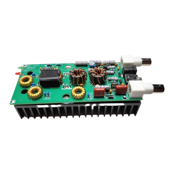
Summary of Contents for QRP Labs QCX 50W Amp
- Page 1 50W HF QCX Power Amplifier kit assembly manual A low-cost, 50W Power Amplifier for the QCX with Full- break-in (QSK) solid state Tx/Rx switching PCB Rev 2 Designed and produced by QRP Labs, 2019 50W QCX PA kit assembly 1.00q...
-
Page 2: Table Of Contents
Contents 1. INTRODUCTION – PCB Rev 2............................4 2. GENERAL ASSEMBLY GUIDELINES..........................4 3. ASSEMBLY..................................5 3.1 Parts list.................................6 3.2 Trace diagram and parts layout...........................10 3.3 Wind and install output transformer T3......................10 3.4 Wind and install Low Pass Filter inductor L6.......................13 3.5 Wind and install Low Pass Filter inductors L4 and L7..................14 3.6 Wind and install bifilar transformer T2........................14 3.7 Wind and install trifilar transformer T1.......................17 3.8 Install Low Pass Filter capacitors C14 and C18....................19... - Page 3 4 NO ENCLOSURE OPTION: PA Transistor installation....................35 5 ENCLOSURE OPTION installation..........................37 6 CIRCUIT EXPLANATION...............................42 6.1 Schematic................................42 6.2 Input attenuator..............................44 6.3 Power Amplifier..............................44 6.4 Thermal considerations............................50 6.5 Low Pass Filter..............................52 6.6 Transmit / Receive switching..........................53 7 Amplifier set-up and operation..........................64 7.1 PA Precautions..............................64 7.2 Power supply...............................65 7.3 Connection to QCX..............................65 7.4 Adjustment................................66...
-
Page 4: Introduction - Pcb Rev 2
You may build it for other bands by suitable choice of low pass filter components; the LPF component values should be the same as in the QCX kit http://qrp-labs.com/qcx, or the QRP Labs LPF kit http://qrp-labs.com/lpfkit. T50 sized toroids must be used, and NP0/C0G type capacitors with at least 100V rating, sufficient to handle the 50W output power. -
Page 5: Assembly
you can easily identify any dry joints or solder bridges before they become a problem later on when you are trying to test the project. Triple check every component value and location BEFORE soldering the component! It is easy to put component leads into the wrong holes, so check, check and check again! It is difficult to de-solder and replace components, so it is much better to get them correctly installed the first time. -
Page 6: Parts List
3.1 Parts list This parts list shows the through-hole components to be inventoried and installed in the assembly. Resistors R1, 6, 9 1K 1W, brown-black-red-gold OR brown-black-black-brown-brown (3pcs) R2, 4 330-ohm, 2W, orange-orange-brown-gold OR orange-orange-black-black-brown (2pcs) 22-ohm, 2W, red-red-black-gold OR red-red-black-gold-brown 4.7K trimmer potentiometer R7, 10, 11, 14, 17 10K, ¼W, brown-black-black-red-brown (5pcs) - Page 7 0.6mm diameter wire Enameled wire (320cm) X1, 3 BNC Connector (2pcs) 3.5mm stereo jack socket 2.1mm DC barrel power connector TO220 insulating silicone pad (2pcs) Insulating washer 2pcs white plastic insulating washer 9mm M3 screw Pan-head screw (2pcs) 6mm M3 screw Pan-head screw (4pcs) Heatsink 130mm x 28mm x 25mm deep (2pcs)
- Page 8 50W QCX PA kit assembly 1.00q...
- Page 9 50W QCX PA kit assembly 1.00q...
-
Page 10: Trace Diagram And Parts Layout
3.2 Trace diagram and parts layout Red = Top side; Blue = bottom side; Green = pads. There are only two layers (nothing is hidden in the middle). Not shown in these diagrams are the extensive ground-planes, on both sides of the board. Practically everything on both layers that isn’t a RED or BLUE track, is ground-plane! The two ground-planes are connected at frequent intervals (not more than 0.1-inches) by vias. - Page 11 I recommend taping the two tubes together using electrical tape; it just helps keep everything nicely held together while winding the turns. An alternative would be to epoxy glue the two tubes together (photo, right). The turns ratio of the transformer (and the actual number of turns) is 2:3.
- Page 12 Cut the wires so that the binocular core body stands elevated 5mm from the workbench (below left). Then scrape the enamel from 5mm of the wire ends, and tin (below right). Install the transformer in the PCB as shown in red (below). Be VERY sure that the 2-turn primary winding wire ends are on the right side, nearest to the transistors Q1 and Q2;...
-
Page 13: Wind And Install Low Pass Filter Inductor L6
3.4 Wind and install Low Pass Filter inductor L6 Measure and cut 34cm of the 0.6mm wire for winding inductor L6 which is wound on a T50-6 toroid (yellow). The number of turns and inductance of L6 is given in the table below: Band Turns Inductance... -
Page 14: Wind And Install Low Pass Filter Inductors L4 And L7
3.5 Wind and install Low Pass Filter inductors L4 and L7 Measure and cut two 30cm lengths of the 0.6mm wire for winding inductors L4 and L7. These two inductors are wound on T50-6 toroids (yellow). The number of turns and inductance of L4 and L7 are given in the table below: Band Turns... - Page 15 The bifilar wire should end up looking something like this (top scale in inches, bottom scale in cm): Wind 10 turns around one of the ferrite toroids (remember, each time the wire passes through the center counts as one turn). Leave 4-5cm of wire at each end. Try to wind the wire tightly on the toroid but be careful not to scratch the enamel which could cause short circuits between the wires.
- Page 16 The diagram and explanation below illustrates the correct wire placement. It is CRITICALLY IMPORTANT to get this right! Now lay the toroid down flat on the table as shown and identify the wires which come from the center of the core, over the top of the outside of the core;...
-
Page 17: Wind And Install Trifilar Transformer T1
on the PCB. Hold the iron on the joint for at least 10 seconds and then feed in some more fresh solder. This should ensure a good joint and all the enamel burned away. Now similarly cut, prepare and solder the other “black marked” wire, which is the one in the hole nearest to C7. - Page 18 This photograph (right) illustrates the process. Prefixes T (for Top) and B (for Bottom) are used to indicate whether the wire comes out from the top side or the bottom side of the toroid when it is laying flat on the table. Wires T-0 and B-0 have continuity.
-
Page 19: Install Low Pass Filter Capacitors C14 And C18
and check for DC continuity (zero resistance). If you do not get zero resistance, then either you have installed the wires in the wrong holes, or you have failed to burn off all the enamel and achieve good joints to the wire. Fix it before proceeding! Next repeat the cut/tin/solder procedure for wires T-1 and B-1. -
Page 20: Install Low Pass Filter Capacitors C11 And C12
3.9 Install Low Pass Filter capacitors C11 and C12 These two capacitors are 250V NP0/C0G types. The capacitor value depends on the band the 50W PA kit is being built for, as follows: Band Value Code 680pF “681” 680pF “681” 390pF “391”... -
Page 21: Install Low Pass Filter Capacitors C19 And C20
3.10 Install Low Pass Filter capacitors C19 and C20 These two capacitors are 250V NP0/C0G types. The capacitor value depends on the band the 50W PA kit is being built for, as follows: Band Value Code 390pF “391” Not installed 180pF “181”... -
Page 22: Install Low Pass Filter Capacitors C9 And C21
3.11 Install Low Pass Filter capacitors C9 and C21 (80m only) These two capacitors are 250V NP0/C0G types. The value is 180pF (code “181”) and capacitors are ONLY installed for the 80m version of the kit. 3.12 Install capacitors C1, 2, 3, 6, 7, 13 and 16 These are 1uF 50V ceramic capacitors, code “105”. -
Page 23: Install Capacitors C4 And C5
3.13 Install capacitors C4 and C5 These are 22nF (0.022uF) 50V ceramic capacitors, code “223”. 3.14 Install capacitors C8 and C10 These are 250V NP0/C0G types with value 47pF, code “470”. 50W QCX PA kit assembly 1.00q... -
Page 24: Install Diodes D2, 4, 6, 8, 9 And 10
3.15 Install diodes D2, 4, 6, 8, 9 and 10 These are 1N4148 diodes. The orientation is important! Bend the wires as shown. Install all the diodes in a row, with the black stripe on the diode body facing the lower edge of the board, so that the black stripe is aligned with the corresponding white stripe on the silkscreen printing. -
Page 25: Install Inductors L1, 2, 3, 5, 8, 9 And 10
3.17 Install inductors L1, 2, 3, 5, 8, 9 and 10 These are 47uH axial molded inductors. Bend the leads as shown and install carefully. 3.18 Install resistors R7, 10, 11, 14 and 17 These are 10K ¼W resistors, colour code brown- black-black-red-brown. -
Page 26: Install Resistor R15
3.19 Install resistor R15 This is a 1.5K resistor, colour code brown-green-red-gold or brown-green-black-brown-brown. 3.20 Install resistor R16 This is a 470-ohm resistor, colour code yellow-purple-black-black-brown. 50W QCX PA kit assembly 1.00q... -
Page 27: Install Resistor R8
3.21 Install resistor R8 This is a 470K resistor, colour code yellow-purple-yellow-gold or yellow-purple-black-orange- brown. 3.22 Install transistor Q3 This is the FQPF2N60C MOSFET in an all-plastic TO220 package, which is installed on the underside of the PCB. It is important to install the transistor with the correct orientation as shown. -
Page 28: Install Transistor Q4
3.23 Install transistor Q4 This is an IRFu9024 transistor in an SMD-leaded package which is installed here like an ordinary through-hole transistor. Make sure the transistor is aligned correctly: the metal face of the transistor must match the thick white line on the PCB silkscreen print. 3.24 Install transistors Q5 and 6 These are BS170 MOSFETs in TO92 packages. -
Page 29: Install Ic1
3.25 Install IC1 IC1 is a 5V voltage regulator, type 78L05, in a TO92-like package. The middle pin needs to be pushed forward slightly to match the holes in the triangular pattern on the PCB. Make sure the flat of the IC body is aligned perfectly with the flat on the PCB silkscreen. It’s not necessary to push the IC all the way in, a lead length of 5mm or so is fine. -
Page 30: Install Resistors R12 And R13
3.27 Install resistors R12 and R13 These are 470-ohm 2W resistors with colour code yellow-purple-brown-gold or yellow-purple- black-black-brown. 3.28 Install resistor R3 This is a 22-ohm 2W resistor, colour code red-red-black-gold or red-red-black-gold-brown. 50W QCX PA kit assembly 1.00q... -
Page 31: Install Resistors R2 And 4
3.29 Install resistors R2 and 4 These are 330-ohm 2W resistors, colour code orange-orange-brown-gold or orange-orange-black- black-brown. 3.30 Install trimmer resistor R5 This is a 4.7K linear trimmer potentiometer. Push the potentiometer pins gently but firmly into the PCB and solder the three terminals. 50W QCX PA kit assembly 1.00q... -
Page 32: Install Capacitors C15 And 17
PCB silkscreen. This is particularly important if you are planning to install the amplifier in the optional QRP Labs enclosure, so that the plug barrel fits through the hole in the rear panel and into the socket. If the alignment is not accurate, the hole and the barrel will not line up correctly. -
Page 33: Install Connector X2: Ptt (Key)
PCB silkscreen. This is particularly important if you are planning to install the amplifier in the optional QRP Labs enclosure, so that the socket barrel fits through the hole in the rear panel. If the alignment is not accurate, the hole and the barrel will not line up correctly. -
Page 34: Install Leds D11 And 12
LED body. Do the same thing for both LEDs. Install the LEDs as pictured, sitting with their flats right on the PCB. This will ensure that if used with the optional QRP Labs enclosure, the LEDs will align perfectly with the holes in the enclosure front panel. -
Page 35: Enclosure Option: Pa Transistor Installation
If you did NOT purchase the enclosure, now is the time to install the IRF510 transistors, Q1 and Q2. Only if NOT using the QRP Labs enclosure! Bend the pins upward of the IRF510 90-degrees right at the body of the IRF510. - Page 36 Position the heatsinks side-by-side as shown below: Apply the blue silicone pads as shown here: Bolt the PA assembly to the heatsinks with two bolts with insulating white plastic washers (see right). The only mounting point in this case is the IRF510 tabs. This is not ideal mechanically and you really should consider using a proper enclosure.
-
Page 37: Enclosure Option Installation
The final completed 50W Amplifier kit should look like this: ENCLOSURE OPTION installation When using the QRP Labs enclosure designed specifically for this 50W PA kit, the IRF510 power transistors must first be bolted to the enclosure assembly, BEFORE soldering to the PCB. - Page 38 Place the heatsinks side-by-side as shown. The enclosure top will be bolted to the heatsinks with 6mm M3 screws in holes 1, 2, 5 and 6. Holes 3 and 4 will be used to bolt the IRF510’s to the heatsink. The remaining holes of the heatsink are not used in this application. Bolt the heatsinks to the outside surface of the top of the enclosure using two 6mm M3 screws on the right-hand side (holes 5 &...
- Page 39 Place the IRF510 transistors through the PCB holes on the underside of the PCB, as shown below. DO NOT SOLDER! Turn over the heatsink/enclosure lid assembly, and slide the PCB carefully and slowly into the slots in the enclosure. The PCB slots are shown here (right). By having the PCB upside-down the IRF510 transistors (which are NOT yet soldered) will fall away from the enclosure lid, allowing them...
- Page 40 It’s worthwhile trying to shine a strong light down and eyeball that narrow gap between PCB and enclosure, to see if it seems that everything is still in place (specifically: those silicone pads). Now insert the final four screws. STILL DO NOT SOLDER THE IRF510’s! The screws at the IRF510 tabs are 9mm M3 screws with the plastic insulating washer (see right).
- Page 41 you have already soldered the center pin, you are at risk of creating a solder bridge and they are quite hard to remove. Similarly, solder the leftmost pin of Q1 first (ground), followed by the center pin then the right pin. Check with the DVM for no short-circuits, AGAIN, after soldering.
-
Page 42: Circuit Explanation
The final step in the enclosure assembly is the addition of the four self-adhesive rubber cabinet feet on the bottom, one in each corner. See photograph below. CIRCUIT EXPLANATION The designer, Hans Summers G0UPL explains some of the details behind the circuit and choices made in the design and production of the kit. - Page 43 50W QCX PA kit assembly 1.00q...
-
Page 44: Input Attenuator
6.2 Input attenuator The pi-network consisting of R2, R3 and R4 forms an attenuator. This is necessary because the output of the QCX will be approximately 5W into 50- ohms; this is a sinewave with 45V peak-peak. This will be too high for the Gate-Source voltage specification (+/- 20V) of the IRF510 transistors. - Page 45 The Vishay IRF510 datasheet for example, specifies V minimum 2.0V, maximum 4.0V. Quite a wide range. It is instructive to compare this schematic to the schematic of the PA section for the QRP Labs 10W Linear kit http://qrp-labs.com/linear (that amplifier is designed for 160m to 10m operation) and discuss the differences in gate bias arrangements.
- Page 46 Next consider the bias adjustment circuits. There are two identical circuits, each one consists of a trimmer potentiometer powered by “BIAS+” which is a 5V regulator. There is a 0.1uF decoupling capacitor at the wiper; then a 47-ohm resistor and 1uH inductor in series to the transistor gate. Additionally the gate drive must be AC coupled to the phase splitting transformer by a DC-blocking 0.1uF capacitor.
- Page 47 The presence or absence of the series inductor from potentiometer wiper to the transistor gates didn’t seem to make much difference one way or the other. Some benefit was provided by using the single trimmer potentiometer bias feeding method but there was a really significant improvement in NOT having the 0.1uF decoupling capacitor at the trimmer wiper! It made a significant improvement in both efficiency and in power output.
- Page 48 maximum junction temperature”. Since the drain current in this application is NOT in fact continuous (it is an RF cycle, and each transistor conducts for half the RF cycle), one might argue that the permissible rating is higher than 5.6A (25C) / 4.0A (100C). In any event, we can see that higher current will eventually kill the transistor so increasing the impedance ratio has limitations.
- Page 49 DC was power supplied by a variable regulated 0-30V 5A bench power supply. A QRP Labs 50- ohm dummy load kit was used as the load (drastically overloaded, but only for very short periods, enough to make the measurement). Power measurements are made by observation of the peak- peak voltage on an oscilloscope.
-
Page 50: Thermal Considerations
Mike builds a broadband HF amplifier stating “with only 1W of drive, you’ll get over 40W out – from 160 through 10 meters!”. He uses two IRF510 transistors with 2:3 turns output transformer, a very similar arrangement to the QRP Labs 50W amplifier. See http://qrp- labs.com/qcx/qro... - Page 51 heat in the IRF510s which has to be dissipated otherwise they will overheat and die fast. That means 25W per device (this assumes equal power distribution between the two devices; in reality there will be variations of characteristics between them so the situation will be worse than this for one of them, and better than this for the other).
-
Page 52: Low Pass Filter
Here, our PA is operated in Class-C, which is not linear. Therefore we use a 7-element Low Pass Filter design which is well tried and tested, and is the same design as used in the QCX transceiver itself, and in the QRP Labs LPF kit http://qrp-labs.com/lpfkit. -
Page 53: Transmit / Receive Switching
Note that the first versions of my 50W Power Amplifier development used inductors I wound using 1.6mm enameled copper wire on sawn-off 5cm (2-inch) sections of broom handle. The first prototype PCB, I thought it would be neat, and interesting, and rather unusual and different, to remind ourselves of how the old-timers used to wind coils. - Page 54 Of critical importance out of these disadvantages, was the cost, and the speed of operation. A key design criteria for me was to be able to switch back and forth between transmit and receive in a very short time, so as to allow full break-in operation (QSK) where the other station is audible between the transmission of your own CW dits and dahs.
- Page 55 The important point is that this undoped “intrinsic layer” acts like a storage reservoir. When incoming forward-biased current arrives, this “intrinsic layer” fills up with electrons. When the diode is reverse biased, it takes time for all these electrons to empty out of the intrinsic layer. At high enough frequencies, the time available is too short! So the diode never “turns off”.
- Page 56 provides 137dB of isolation in the “Off” state. Amazing! We don’t need anything so extreme (or complex) here – but the principles are well described by W6JL and his work is inspiring. It is possible to distill the whole topic into two important rules: To switch the PIN diode Off, apply a large reverse bias VOLTAGE.
- Page 57 To switch ON the diode D1, we arrange for a forward bias CURRENT to flow through D1. For this, we set A to the supply voltage, and B to ground. The current flows through the diode, limited only by R1. Using Ohm’s law (I = V / R) with 12V supply voltage leads to a current of 12 / 1000 = 12mA (neglecting voltage drop across the diode and other losses).
- Page 58 The solution was to change it to 0.33uF and a proper low loss NP0 type with Class-I dielectric, which is a not-too-expensive high voltage capacitor at DigiKey, and has low enough loss not to dissipate power and overheat. This is the reason why both C15 and C17 are 0.33uF capacitors. The forward bias current in D7 is determined here by R13 (470-ohms) is 25mA at 12V, rising to 42mA at 20V supply.
- Page 59 power amplifier. Actually, two diodes back-to-back is probably overkill. One diode should provide sufficient Off isolation. But during the development I was plagued by huge spurious bursts at the instant of transmit/receive switchover – exactly as described by Pat G3VA (SK, RIP)! This was very difficult to tame, but very educational –...
- Page 60 To get things started, in the absence of any signal, I also pass in the supply voltage via D6/8. That ensures that the switch is “off” even when there is no RF signal. What about the fact that the diodes are all implemented by two 1N4148 diodes in series? Why? Because, according to the datasheet (Vishay, but all the manufacturers are similar), the absolute maximum rating for a 1N4148 “Repetitive peak reverse voltage”...
- Page 61 Source voltage as 60V DC. Well – here we are applying much more than that! More like ~150V DC! Severe abuse of the BS170! The phenomenon seen in the ‘scope trace is known as Avalanche Breakdown. A quote from Wikipedia https://en.wikipedi0.org/wiki/Avalanche_breakdown: “Avalanche breakdown is a phenomenon that can occur in both insulating and semiconducting materials.
- Page 62 One final problem in the Transmit / Receive switching consumed a good solid 2 days of investigation, and was both highly educational, interesting and satisfying to solve. This problem is shown here in a photograph of the oscilloscope screen, which shows a single Morse code “dit”...
- Page 63 And Pat Hawker G3VA (RIP) would surely be have been horrified had he heard of QRP Labs doing such a thing. The cause is easy to explain now, but was very hard to find, at the time. I tried adding things here and there, and I could change the shape of the spike.
-
Page 64: Amplifier Set-Up And Operation
Dealing first with the Receive → Transmit transition; PTT is initially at 0V. The transistors Q5 and Q6 (above left) are therefore OFF. The Q5 gate is connected to PTT so when PTT goes to +5V (on key-down), Q5 is switched on; this pulls the gate of Q3 to ground (0V) so Q3 is switched off. With Q5 on and Q3 off, reverse bias voltage is applied to diodes D3 and D5, causing them to be switched OFF;... -
Page 65: Power Supply
5) On first powering up the amplifier, and during adjustments, use a current-limited supply. If anything does go wrong, you’ll have more time to notice it before letting the smoke out. 7.2 Power supply For full 50W power output the PA requires a supply of 20V at about 5 or 6A. Ensure you are using a power supply which is up to the job! The power supply needs to be capable of supplying full current suddenly without any voltage drop on key-down. -
Page 66: Adjustment
The output of the 50W Power Amplifier connects directly to the antenna system – which could include matching units or tuners. Do not transmit at full power into a mismatched (high SWR) antenna system. It is strongly recommended to connect a 10K resistor in the QCX from IC3 pin 13 to IC3 pin 14. This modification is detailed further, here: http://www.qrp-labs.com/qcx/qcxmods/ptt.html 7.4 Adjustment... -
Page 67: Measurements
Similarly do NOT operate at a setting of R5 beyond the recommended setting (see previous section). A higher setting (more clockwise) can produce more power output for a given supply voltage, but it also increases the risk of spurious output and glitches. Measurements 8.1 Power output vs Supply voltage This is a measurement of output power vs supply voltage for the production models assembled for... -
Page 68: Low Pass Filter Characteristics
8.2 Low Pass Filter characteristics These measurements show the filter characteristic of the Low Pass Filter section only. An Advantest R3361C Spectrum Analyzer with Tracking Generator was used. BNC connectors were soldered to the LPF filter and output and connected to the spectrum analyzer using 50-ohm coaxial cables. -
Page 69: Version History
This is a zoom on the trailing edge (key-up) with 1ms/division setting on the oscilloscope. Version History 1.00 12-Dec-2019 First version 1.00a 12-Dec-2019 Added missing values for 30m LPF inductors 1.00b 12-Dec-2019 Correct wrong title of section 3.13 1.00c 13-Dec-2019 One wrong diagram in the description of switch SW3 1.00d 13-Dec-2019... - Page 70 1.00j 06-Jan-2020 Fix typo (0.1uF should be 1uF, thanks Jon W8REA) Continuity test wrong in 3.6 (thanks Paul AI4EE & George SV2SBE) 1.00k 01-Jun-2020 Corrected C/W typo on page 50; edited page 56 explanation about overheating capacitors, which are not caused by reactance.
Need help?
Do you have a question about the QCX 50W Amp and is the answer not in the manual?
Questions and answers