
Related Manuals for Samsung HC-R4241W


Summary of Contents for Samsung HC-R4241W
-
Page 1: Table Of Contents
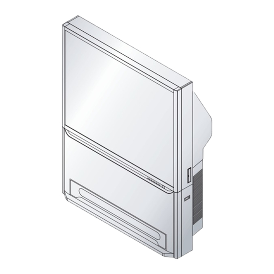
PROJECTION TV RECEIVER Chassis : P60B(N)_Omega-2 Model : SP54T8HL1X/XAX SERVICE Manual PROJECTION TV RECEIVER CONTENTS Product Specification Alignment & Adjustment Troubleshooting Exploded View & Part List Electrical Part List PCB Diagram Schematic Diagram... -
Page 2: Product Specification
Product Specification 1. Product Specification Model HC-R4241W HC-R4741W HC-R4351W HC-R4751W Voltage AC 120V Frequency of 60Hz Operation Power Consumption 240 watts Dimension 1004 x 500 x 967 mm 1126 x 621 x 984 mm 1035 x 510 x 888 mm... - Page 3 MEMO Samsung Electronics...
-
Page 4: Alignment & Adjustment
Direction keys ◀ / ▶ 2-1-4 Cautions Regarding service Mode 1. Do not adjust the fixed attributes, only the adjustables. 2. For adjustments of RF and 1080i Modes, switch to the respective input source and proceed with the adjustments. Samsung Electronics... - Page 5 0 ~ 63 12 H Trapezium 0 ~ 63 13 Bow 0 ~ 63 14 Angle 0 ~ 63 15 V Position 0 ~ 63 16 CXA Left Blk 0 ~ 63 17 CXA Right Blk 0 ~ 63 Samsung Electronics...
- Page 6 -63 ~ 63 12 H Trapezium -63 ~ 63 13 Bow -63 ~ 63 14 Angle -63 ~ 63 15 V Position -63 ~ 63 16 CXA Left Blk -63 ~ 63 17 CXA Right Blk -63 ~ 63 Samsung Electronics...
- Page 7 12 NR Hight Ref (s) 0 ~ 127 13 NR Low Ref (s) 0 ~ 127 14 NR Hight Value (s) -128 ~ 127 15 NR Low Value (s) -128 ~ 127 16 NR Read M/S Read Data Samsung Electronics...
- Page 8 0~ 13 14 CTI Level 0 ~ 3 15 COL AXIS 0 ~ 3 16 LTI Level 0 ~ 3 17 9405 U-OUT 0 ~ 255 18 9405 Y-OUT 0 ~ 255 19 9405 V-OUT 0 ~ 255 Samsung Electronics...
- Page 9 13 SHP f1 & P/O 0 ~ 15 13 (ALL-mode) 14 AKB Time 0 ~ 31 15 YC Delay 0 ~ 31 16 PIP YC Delay 0 ~ 31 17 BandPass 9407 0 ~ 7 18 HighPass 9407 0 ~ 7 Samsung Electronics...
- Page 10 12 S-ABL 0 ~ 3 13 P_ABL 0 ~ 2 14 PLIMT_LEV 0 ~ 2 15 AKB 0 ~ 1 16 CLP Gate 0 ~ 1 17 Color Kil 0 ~ 255 18 Real Time(Hour) 0 ~ 255 Samsung Electronics...
- Page 11 0 ~ 7 S-Video 14 IF_Comp_DVD 0 ~ 7 15 VM_Delay_480p 0 ~ 3 480p 16 1E Data1 9405 0 ~ 15 All-Mode 17 1E Data2 9405 0 ~ 15 All-Mode 18 1E Data3 9405 0 ~ 15 All-Mode Samsung Electronics...
- Page 12 11 DCE Gain 0 ~ 255 12 CTI Gain 0 ~ 15 13 DEP TH Cor 0 ~ 63 14 DEP OV Gain H 0 ~ 255 15 DEP R INT 0 ~ 127 16 CTE Gain 0 ~ 255 Samsung Electronics...
- Page 13 12 No Sync Mute On ↔ Off 13 AGC On ↔ Off 14 Turbo Effect On ↔ Off 15 Burst Screen On ↔ Off 16 LNA On ↔ Off 17 Pixelshift 1 ~ 5, Off 18 PS Time(MIN) 1,30,60,Off 2-10 Samsung Electronics...
- Page 14 Alignment & Adjustment 2-3 Screen Change (When adjusting I2C Bus Geometric items) V SIZE V SHIFT V LINEARITY V - S - CORRECTION H SIZE PIN PHASE PIN AMP H SHIFT V BOW V ANGLE Samsung Electronics 2-11...
- Page 15 8. Select R-drive, G-drive, and B-drive by pressing the keys. 9. Adjust the high light with viewing the light side of the screen. 10. If necessary, redo screen adjustments and 6~9. 11. Press the Add key to exit. 2-12 Samsung Electronics...
- Page 16 (Repeat if unsuccessful, varying the VR of the front Focus Pack.) ⑤ Perform steps 1~3 for the R and B Lenses. 3. Note Green determines picture quality; pay close attention for exact adjustment. < _ L1, L2 Fig. 2-2 Color Aberration Samsung Electronics 2-13...
- Page 17 13. Adjust the Focus-pack VR for fine focusing. 14. Press the 7- digit button for a while, on the remote control, and the mode changes to the Convergence Adjustment mode. 15. Press the "S.MODE" Key on the remote control to return to normal viewing. 2-14 Samsung Electronics...
- Page 18 Screen Size : X 925, Y 523 (X: 378 =9*2 + 30*12 , Y:440=28* 2+64* 6) 22.02mm 73.41mm 22.02mm 33.28mm 76.07mm 33.28mm 2-6-2 4241W DTV Mode Screen Size : X 925, Y 523 (X: 396 =12*2 + 31* 12, Y : 488= 40* 2+68* 6) 28.03mm 72.41mm 28.03mm 42.87mm 72.88mm 42.87mm Samsung Electronics 2-15...
- Page 19 Alignment & Adjustment 2-6-3 4351W RF Mode 23.89mm 75.44mm 23.89mm 34.84mm 77.89mm 34.84mm 2-6-4 4351W DTV Mode 31.59mm 74.19mm 31.59mm 35.50mm 77.67mm 35.50mm 2-16 Samsung Electronics...
- Page 20 Screen Size : X 1045, Y 588 (X: 378 =9*2 + 30*12 , Y:440=28* 2+64* 6) 24.88mm 82.94mm 24.88mm 37.42mm 85.53mm 37.42mm 2-6-6 4741W DTV Mode Screen Size : X 1045, Y 588 (X: 396 =12*2 + 31* 12, Y : 488= 40* 2+68* 6) 31.67mm 81.81mm 37.67mm 48.20mm 81.93mm 48.20mm Samsung Electronics 2-17...
- Page 21 Screen Size : X 1153, Y 649 (X: 378 =9*2 + 30*12 , Y:440=28* 2+64* 6) 27.45mm 91.51mm 27.45mm 41.3mm 94.4mm 41.3mm 2-6-8 5241W DTV Mode Screen Size : X 1153, Y 649 (X: 396 =12*2 + 31* 12, Y : 488= 40* 2+68* 6) 34.94mm 90.26mm 34.94mm 53.20mm 90.43mm 53.20mm 2-18 Samsung Electronics...
- Page 22 (Backwards: Left or Up) RF mode Moves the Convergence Pattern to the left Save data after completing Convergence Adjustment Automatic Convergence Adjustment after completing Convergence Adjustments (Automatic Color Adjustment to compensate for the earth s magnetic field.) Samsung Electronics 2-19...
- Page 23 14. "MUTE" Key : Move Cursor Forward Key Press to move the cursor right or down. 15. "∧,∨,+,-" Key : Convergence Picture Move Button Use the Channel button (∧,∨) to adjust Convergence Data up/down and use the Volume buttons (+, -) for left/right adjustment. 2-20 Samsung Electronics...
- Page 24 White Cross on the background 5-435 ++++ (43Q5HL1) 43Q5HL1X (white cross) 47" (4741W) 4741WX White Cross on the background 5-472 ++++ (47Q2HL1) 47Q2HL1X (white cross) 52" (5241W) 5241WX White Cross on the background 5-522 ++++ (52Q2HL1) 52Q2HL1X (white cross) Samsung Electronics 2-21...
- Page 25 4. Press R-MUTE "+100" key and B-MUTE "PRE-CH" key to mute out Red and Blue. Press G-SELECT "8" key to adjust the Green Color Convergence first. (For the first entrance, Green Color Convergence will automatically be selected.) 5. Press the "MUTE" key to move the cursor right, the "P.MODE" button to move the cursor left. 2-22 Samsung Electronics...
- Page 26 7. For vertical moves, select "SOUREC" key and press "MUTE" key to move down, and "P.MODE" key to move down. Caution : Pressing the "SOUREC" key again will switch to horizontal movement. 8. Use the Line Move Key "4" for global shaping in the beginning stages of Convergence Adjustment. Moves Entire Line Samsung Electronics 2-23...
- Page 27 Caution : The Cursor will move to the center and blink two times before it automatically moves back to its original position. Caution : After completing and saving the R, G and B Convergence Adjustment , the data should be saved by pressing the "SELF FOCUS" button before exiting Convergence Mode. 2-24 Samsung Electronics...
- Page 28 1. After completing the Convergence Adjustment, press the Memory button "ADD/DEL" key to save the data and exit back to a black screen. Then enter Convergence Mode again to do the Automatic Color Adjustment by pressing the "Automatic Color Adjustment" button. Up / Down Left / Right Samsung Electronics 2-25...
- Page 29 Alignment & Adjustment 2-8 Pin Spec 2-8-1 Convergence Module CNZ01 Name Name D-FOCUS D2(SCL) C-SYNC CG-R CG-G H-BLK CG-B V-BLK D3(SDA) F-BLK 5V-CG 2-26 Samsung Electronics...
-
Page 30: Troubleshooting
3-1 Opening the Set and Replacing Assemblies 3-1-1 Replacing and Repairing Each Assembly (Opening the Back Cover) Remove all indicated screws on the rear side of the Set Repair or replace the required Assembly CG Module MAIN DY JACK Samsung Electronics... - Page 31 Troubleshooting 3-1-2 Replacing and Repairing the CRT-PCB (Opening the Rear Cover) Remove all indicated screws and open the Front Cover. Repair the frontal PCB-CRT or replace it after removing the attached connectors PCB-CRT R PCB-CRT G PCB-CRT B Samsung Electronics...
- Page 32 Remove the screws indicated and detach the Top Cover Remove the Dust Cover that prevents dust from entering into the screen Before proceeding, disconnect all the DY and Connectors connected to the assembly. Remove the 4 corner screws from the CRT and replace the CRT Samsung Electronics...
- Page 33 CN801 and CN802 on the SUB Board Normal Abnormal Abnormal Check the output terminal of CNZ02 (BV,BH,RV,RH,GV,GH) Normal Validate the H-BLK and V-BLK outputs of the MAIN Board Check the respective circuits regarding the symptoms Replace the Convergence Module Samsung Electronics...
- Page 34 Check FD802S of the SUB Board Check IC601 Input Terminal Pin 5 Abnormal Normal Check the Sound Mute Circuit Check IC601 Input Terminal Pins 7 and 11 Normal Abnormal Check IC601 Check IC602 Input Terminals Normal Abnormal Check IC602 Check IC605 Input Terminals Samsung Electronics...
- Page 35 Check CN501 Pins 1, 3, and 5 Normal Check IC501, 531, and 561 Abnormal Check the CN501 Connector Abnormal Normal Replace the CN501 Connector Check IC04 Input Terminal Pins 20, 21 and 22 Normal Check IC04 Abnormal Check IC03 Samsung Electronics...
- Page 36 Troubleshooting Check the Heater (Abnormal) Abnormal Replace R513, 543 and 573 Normal Replace R513, 543 and 573 Abnormal Check CB504 Pin 5 of the CRT-PCB Check R464 Samsung Electronics...
- Page 37 MEMO Samsung Electronics...
-
Page 38: Exploded View & Part List
S.N.A T0016 T0299 AA91-00887A ASSY-HOLDER,MIRROR(R);,HIPS HB BLK,INLAY S.N.A T0324 BP96-00226E ASSY COVER P-WOOD;54T8,WOOD,J60A S.N.A T0269 T0600 AA60-00072B SPACER-COVER,DUST;43,54,62J9,SPONGE 94HF T0601 BP91-01588A ASSY PRT;SP54T8HLX/XAP,P60A S.N.A T0929 BP61-00818A HOLDER-MIRROR,BOTTOM;PJTV,HIPS HB,T3.0,B T0962 BP64-00153E CABINET BACK-SIDE R;54T8,HIPS,HB,GR503 T0962 BP64-00153F CABINET BACK-SIDE L;54T8,HIPS,HB,GR503 Samsung Electronics... -
Page 39: Electrical Part List
...4 C125 2401-000913 C-AL;22uF,20%,16V,GP,TP,5x11,5 ...4 MR815 2003-001091 R-METAL OXIDE(S);10ohm,5%,2W,AF,TP,4x12m ...4 C134 2401-000913 C-AL;22uF,20%,16V,GP,TP,5x11,5 ...4 MR814 2003-001098 R-METAL OXIDE(S);22Kohm,5%,3W,AA,TP,6x16 ...4 C135 2401-000913 C-AL;22uF,20%,16V,GP,TP,5x11,5 ...4 R675 2004-000433 R-METAL;1Kohm,1%,1/8W,AA,TP,1.8x3.2mm ...4 C136 2401-000913 C-AL;22uF,20%,16V,GP,TP,5x11,5 ...4 R676 2004-000433 R-METAL;1Kohm,1%,1/8W,AA,TP,1.8x3.2mm ...4 C137 2401-000913 C-AL;22uF,20%,16V,GP,TP,5x11,5 Samsung Electronics... - Page 40 BP97-00914E ASSY SMD-MAIN;USA,P60B S.N.A ..5 FR22 2007-000066 R-CHIP;20Kohm,1%,1/10W,TP,1608 ..5 D902 0401-000132 DIODE-SWITCHING;BAV99,70V,50MA,SOT-23,TP ..5 FR23 2007-000066 R-CHIP;20Kohm,1%,1/10W,TP,1608 ..5 D905 0401-000132 DIODE-SWITCHING;BAV99,70V,50MA,SOT-23,TP ..5 ER04 2007-000070 R-CHIP;0ohm,5%,1/10W,TP,1608 ..5 FD07 0401-000132 DIODE-SWITCHING;BAV99,70V,50MA,SOT-23,TP ..5 ER05 2007-000070 R-CHIP;0ohm,5%,1/10W,TP,1608 ..5 FD09 0401-000132 DIODE-SWITCHING;BAV99,70V,50MA,SOT-23,TP ..5 ER06 2007-000070 R-CHIP;0ohm,5%,1/10W,TP,1608 Samsung Electronics...
- Page 41 2007-000074 R-CHIP;100ohm,5%,1/10W,TP,1608 ..5 R797 2007-000078 R-CHIP;1Kohm,5%,1/10W,TP,1608 ..5 R624 2007-000074 R-CHIP;100ohm,5%,1/10W,TP,1608 ..5 R798 2007-000078 R-CHIP;1Kohm,5%,1/10W,TP,1608 ..5 R625 2007-000074 R-CHIP;100ohm,5%,1/10W,TP,1608 ..5 R905 2007-000078 R-CHIP;1Kohm,5%,1/10W,TP,1608 ..5 R626 2007-000074 R-CHIP;100ohm,5%,1/10W,TP,1608 ..5 R921 2007-000078 R-CHIP;1Kohm,5%,1/10W,TP,1608 ..5 R627 2007-000074 R-CHIP;100ohm,5%,1/10W,TP,1608 ..5 R924 2007-000078 R-CHIP;1Kohm,5%,1/10W,TP,1608 Samsung Electronics...
- Page 42 2007-000123 R-CHIP;1.5Kohm,5%,1/10W,TP,1608 ..5 EC69 2203-000181 C-CER,CHIP;100nF,+80-20%,25V,Y5V,TP,2012 ..5 FR46 2007-000124 R-CHIP;2.2Kohm,5%,1/10W,TP,1608 ..5 EC70 2203-000181 C-CER,CHIP;100nF,+80-20%,25V,Y5V,TP,2012 ..5 FR47 2007-000124 R-CHIP;2.2Kohm,5%,1/10W,TP,1608 ..5 EC72 2203-000181 C-CER,CHIP;100nF,+80-20%,25V,Y5V,TP,2012 ..5 FR70 2007-000124 R-CHIP;2.2Kohm,5%,1/10W,TP,1608 ..5 EC73 2203-000181 C-CER,CHIP;100nF,+80-20%,25V,Y5V,TP,2012 ..5 R662 2007-000126 R-CHIP;4.3Kohm,5%,1/10W,TP,1608 ..5 EC75 2203-000181 C-CER,CHIP;100nF,+80-20%,25V,Y5V,TP,2012 Samsung Electronics...
- Page 43 2203-000257 C-CER,CHIP;10nF,10%,50V,X7R,1608 ..5 SC72 2203-001652 C-CER,CHIP;470nF,+80-20%,16V,Y5V,1608 ..5 FC54 2203-000257 C-CER,CHIP;10nF,10%,50V,X7R,1608 ..5 SC73 2203-001652 C-CER,CHIP;470nF,+80-20%,16V,Y5V,1608 ..5 SC13 2203-000257 C-CER,CHIP;10nF,10%,50V,X7R,1608 ..5 SC75 2203-001652 C-CER,CHIP;470nF,+80-20%,16V,Y5V,1608 ..5 SC33 2203-000257 C-CER,CHIP;10nF,10%,50V,X7R,1608 ..5 SC76 2203-001652 C-CER,CHIP;470nF,+80-20%,16V,Y5V,1608 ..5 SC35 2203-000257 C-CER,CHIP;10nF,10%,50V,X7R,1608 ..5 SC77 2203-001652 C-CER,CHIP;470nF,+80-20%,16V,Y5V,1608 Samsung Electronics...
- Page 44 BP97-01009C ASSY AUTO-CG;OMEGA / CHAMP S.N.A ..5 T0568 3301-001324 BEAD-SMD;15ohm,2012,600mA,TP,,,0.1ohm S.N.A ..5 Q409 0505-000109 FET-SILICON;2N7000,N,60V,200mA,5ohm,400m ..5 T0568 3301-001324 BEAD-SMD;15ohm,2012,600mA,TP,,,0.1ohm S.N.A ..5 Q409 0505-000109 FET-SILICON;2N7000,N,60V,200mA,5ohm,400m ..5 T0568 3301-001324 BEAD-SMD;15ohm,2012,600mA,TP,,,0.1ohm S.N.A ..5 2401-000480 C-AL;10uF,20%,50V,GP,TP,5x11,5 ..5 T0568 3301-001324 BEAD-SMD;15ohm,2012,600mA,TP,,,0.1ohm S.N.A ..5 2401-000480 C-AL;10uF,20%,50V,GP,TP,5x11,5 Samsung Electronics...
- Page 45 ..6 R123 2007-000090 R-CHIP;10Kohm,5%,1/10W,TP,1608 ..6 2007-000074 R-CHIP;100ohm,5%,1/10W,TP,1608 ..6 R126 2007-000090 R-CHIP;10Kohm,5%,1/10W,TP,1608 ..6 2007-000074 R-CHIP;100ohm,5%,1/10W,TP,1608 ..6 R127 2007-000090 R-CHIP;10Kohm,5%,1/10W,TP,1608 ..6 2007-000074 R-CHIP;100ohm,5%,1/10W,TP,1608 ..6 R130 2007-000090 R-CHIP;10Kohm,5%,1/10W,TP,1608 ..6 2007-000074 R-CHIP;100ohm,5%,1/10W,TP,1608 ..6 R131 2007-000090 R-CHIP;10Kohm,5%,1/10W,TP,1608 ..6 2007-000074 R-CHIP;100ohm,5%,1/10W,TP,1608 ..6 2007-000090 R-CHIP;10Kohm,5%,1/10W,TP,1608 Samsung Electronics...
- Page 46 RZ108 2001-000241 R-CARBON;1.5KOHM,5%,1/8W,AA,TP,1.8X3.2MM ..6 2203-000204 C-CER,CHIP;100nF,10%,25V,X7R,TP,2012 ...4 RZ118 2001-000258 R-CARBON;1.8KOHM,5%,1/8W,AA,TP,1.8X3.2MM ..6 2203-000204 C-CER,CHIP;100nF,10%,25V,X7R,TP,2012 ...4 RZ117 2001-000258 R-CARBON;1.8KOHM,5%,1/8W,AA,TP,1.8X3.2MM ..6 2203-000204 C-CER,CHIP;100nF,10%,25V,X7R,TP,2012 ...4 RZ107 2001-000331 R-CARBON;12KOHM,5%,1/8W,AA,TP,1.8X3.2MM ..6 2203-000204 C-CER,CHIP;100nF,10%,25V,X7R,TP,2012 ...4 RZ116 2001-000331 R-CARBON;12KOHM,5%,1/8W,AA,TP,1.8X3.2MM ..6 2203-000204 C-CER,CHIP;100nF,10%,25V,X7R,TP,2012 ...4 RZ119 2001-000554 R-CARBON;270OHM,5%,1/8W,AA,TP,1.8X3.2MM Samsung Electronics...
- Page 47 BP41-00172A PCB CONTROL;SP54T8,CONTROL,1L,A,1.6T,245 S.N.A ...4 M0081 6003-000334 SCREW-TAPTITE;RH,+,2S,M3,L6,ZPC(YEL),SWR S.N.A ...4 QY01 0504-001061 TR-DIGITAL;KRC111M,NPN,400mW,10K,TO-92M, ...4 T0175 AA62-00056A HEAT SINK-PS;-,-,T1.0,-,41*35*70,D2,-,-, S.N.A ...4 QY02 0504-001061 TR-DIGITAL;KRC111M,NPN,400mW,10K,TO-92M, ...4 T0088 1204-000517 IC-VERTICAL DEF.;LA7845,SIP,7P,-,PLASTIC T0091 BP94-01405K ASSY PCB MISC-A/V SIDE;SP54T8HL1X/ANB,J6 ...4 CIS1 0205-001154 OIL-SILICON;G746,-,- S.N.A Samsung Electronics...
- Page 48 0403-000708 DIODE-ZENER;MTZJ13B,12.55-13.21V,500mW,D ...4 RZ139 2001-000591 R-CARBON;3.3KOHM,5%,1/8W,AA,TP,1.8X3.2MM ...4 DZ408A 0403-000708 DIODE-ZENER;MTZJ13B,12.55-13.21V,500mW,D ...4 RZ143 2001-000591 R-CARBON;3.3KOHM,5%,1/8W,AA,TP,1.8X3.2MM ...4 DZ803 0403-000716 DIODE-ZENER;MTZJ4.7B,4.59-4.77V,500MW,DO ...4 RZ147 2001-000591 R-CARBON;3.3KOHM,5%,1/8W,AA,TP,1.8X3.2MM ...4 DZ405 0403-000719 DIODE-ZENER;MTZJ7.5B,7.11-7.44V,500MW,DO ...4 RZ167 2001-000702 R-CARBON;39KOHM,5%,1/8W,AA,TP,1.8X3.2MM ...4 DZ304 0403-000734 DIODE-ZENER;TZP15B,14.7-16.5V,1000MW,DO- ...4 RZ168 2001-000702 R-CARBON;39KOHM,5%,1/8W,AA,TP,1.8X3.2MM 5-10 Samsung Electronics...
- Page 49 2201-000376 C-CERAMIC,DISC;0.22NF,5%,50V,SL,TP,6.3X3 ...4 R426 2003-000586 R-METAL OXIDE(S);22Kohm,5%,2W,AF,TP,4x12 ...4 C407S 2201-000406 C-CERAMIC,DISC;0.27NF,10%,2KV,Y5P,TP,6.3 ...4 R318 2003-000690 R-METAL OXIDE(S);4.7ohm,5%,2W,AA,TP,4x12 ...4 C411 2201-000406 C-CERAMIC,DISC;0.27NF,10%,2KV,Y5P,TP,6.3 ...4 R303 2003-001018 R-METAL OXIDE(S);220ohm,5%,2W,AF,TP,3.9x ...4 CS804 2201-000516 C-CERAMIC,DISC;4.7NF,+100-0%,500V,Y5U,TP ...4 RZ151 2003-001024 R-METAL OXIDE(S);150ohm,5%,2W,AF,TP,3.9x ...4 C433 2201-000556 C-CERAMIC,DISC;0.47NF,10%,500V,Y5P,TP,5. Samsung Electronics 5-11...
- Page 50 S.N.A ...4 CZ135 2401-000471 C-AL;10uF,20%,50V,BP,TP,5x11,5mm ...4 EY118 6042-000002 EYELET;ID1.5,OD2,L2.8,NI+SN,BSP3-1/2H S.N.A ...4 C429 2401-000480 C-AL;10uF,20%,50V,GP,TP,5x11,5 ...4 EY119 6042-000002 EYELET;ID1.5,OD2,L2.8,NI+SN,BSP3-1/2H S.N.A ...4 C430 2401-000480 C-AL;10uF,20%,50V,GP,TP,5x11,5 ...4 EY12 6042-000002 EYELET;ID1.5,OD2,L2.8,NI+SN,BSP3-1/2H S.N.A ...4 CS802 2401-000480 C-AL;10uF,20%,50V,GP,TP,5x11,5 ...4 EY120 6042-000002 EYELET;ID1.5,OD2,L2.8,NI+SN,BSP3-1/2H S.N.A 5-12 Samsung Electronics...
- Page 51 6042-000002 EYELET;ID1.5,OD2,L2.8,NI+SN,BSP3-1/2H S.N.A ...4 EY21 6042-000002 EYELET;ID1.5,OD2,L2.8,NI+SN,BSP3-1/2H S.N.A ...4 EY106 6042-000002 EYELET;ID1.5,OD2,L2.8,NI+SN,BSP3-1/2H S.N.A ...4 EY22 6042-000002 EYELET;ID1.5,OD2,L2.8,NI+SN,BSP3-1/2H S.N.A ...4 EY116 6042-000002 EYELET;ID1.5,OD2,L2.8,NI+SN,BSP3-1/2H S.N.A ...4 EY23 6042-000002 EYELET;ID1.5,OD2,L2.8,NI+SN,BSP3-1/2H S.N.A ...4 GT304 BH71-40300A PIN-HINGE;BRASS,D2.36!,HEAT/SINK,SN S.N.A ...4 EY24 6042-000002 EYELET;ID1.5,OD2,L2.8,NI+SN,BSP3-1/2H S.N.A Samsung Electronics 5-13...
- Page 52 2001-000009 R-CARBON;20KOHM,5%,1/8W,AA,TP,1.8X3.2MM ...4 C505 2305-000149 C-FILM,LEAD-PEF;100nF,5%,100V,TP,12x12.5 ...4 R576 2001-000009 R-CARBON;20KOHM,5%,1/8W,AA,TP,1.8X3.2MM ...4 C535 2305-000149 C-FILM,LEAD-PEF;100nF,5%,100V,TP,12x12.5 ...4 R524 2001-000028 R-CARBON(S);100OHM,5%,1/2W,AA,TP,2.4X6.4 ...4 C565 2305-000149 C-FILM,LEAD-PEF;100nF,5%,100V,TP,12x12.5 ...4 R554 2001-000028 R-CARBON(S);100OHM,5%,1/2W,AA,TP,2.4X6.4 ...4 C507 2305-000154 C-FILM,LEAD-PEF;100nF,5%,400V,TP,21.5x6..4 R584 2001-000028 R-CARBON(S);100OHM,5%,1/2W,AA,TP,2.4X6.4 ...4 C537 2305-000154 C-FILM,LEAD-PEF;100nF,5%,400V,TP,21.5x6. 5-14 Samsung Electronics...
- Page 53 S.N.A T0214 AA60-40006A PIN-STAPLE;AUTO,33X17.8X2.4,H18,33X17.8X S.N.A T0069 BN60-00027B SPACER-FELT;PJTV,PRT,FELT,L20,T1.0,W20 S.N.A T0214 AA61-20285A HOLDER-BOX;3456,PP,-,-,-,WHT,VO T0333 BP60-00050A SPACER-CAP;EPDM,BLK T0172 AA69-02609A BAND-PP;W18,CLEA,1G S.N.A T0108 BP61-00079A HOLDER-DY;,PJTV,T0.5,NYLON66 V2 S.N.A T0376 6902-000061 BAG AIR;LDPE,T0.2,L1000,W500,TRP,,, S.N.A T0070 BP96-01011B ASSY COVER P-HOLDER CAP;PJTV,PC CLR,G,B S.N.A Samsung Electronics 5-15...
- Page 54 M0081 6003-001323 SCREW-TAPTITE;BH,+,B,M4,L12,NI PLT,SWRCH S.N.A ...4 T0516 BP61-00447A HOLDER-CASTER;PJTV,HIPS,T1.5,Dia41mm S.N.A T0298 AA61-01116A BRACKET-HINGE;55W9,SECC,T2.0 S.N.A M0156 BP68-00500B MANUAL USERS-01;COMM,SAMSUNG,MEXICAN SPAS.N.A T0211 BP61-00181A BRACKET-DOOR,RACK;54T8,SECC,T1.0 S.N.A BP68-00515A MANUAL-REGISTRATION CARD;PRC CARD,SAMSUN S.N.A CIS1 BP64-00154A CABINET-DOOR,RACK;54T8,HIPS,HB,GRAY T0101 BP64-00208A WINDOW-DOOR RACK;54T8,GLASS,T3.0,,,,BR, S.N.A M0081 6003-001351 SCREW-TAPTITE;FH,+,B,M4,L16,NI PLT,SWRCH S.N.A...
- Page 55 AA61-20284A HOLDER;P-CORD,PP,-,-,-,BLK,VO,KE-002 S.N.A T0603 AA63-10002A BAND-TIE;NYLON66 V2,L100,NTR S.N.A CIS1 AA65-00029A CLAMPER CORE-WIRE;PJTV,NYLON66,OD24,DONG S.N.A CIS1 AA65-30110A CLAMPER CORE-WIRE;ALL MODEL,NYLON 66,V2, S.N.A CIS1 AA65-30111A CLAMPER CORE-WIRE;ALL MODEL,NYLON,V0,-,W S.N.A M2893 BP39-00018A LEAD CONNECTOR;P55A/HCM4215W,UL2547#26,U CIS1 AA65-30105A CLAMPER CORE-WIRE;ALL MODEL,NYLON 66,V2, S.N.A Samsung Electronics 5-17...
- Page 56 MEMO 5-18 Samsung Electronics...
-
Page 57: Pcb Diagram
PCB Diagram 6. PCB Diagram 6-1 MAIN PCB Samsung Electronics... - Page 58 PCB Diagram 6-2 SUB PCB Samsung Electronics...
-
Page 59: Schematic Diagram
Schematic Diagram 7. Schematic Diagram 7-1 MAIN-1 This Document can not be used without Samsung’s authorization. Samsung Electronics... - Page 60 Schematic Diagram 7-2 MAIN-2 This Document can not be used without Samsung’s authorization. Samsung Electronics...
- Page 61 Schematic Diagram 7-3 MAIN-3 This Document can not be used without Samsung’s authorization. Samsung Electronics...
- Page 62 Schematic Diagram 7-4 MAIN-4 This Document can not be used without Samsung’s authorization. Samsung Electronics...
- Page 63 Schematic Diagram 7-5 MAIN-5 This Document can not be used without Samsung’s authorization. Samsung Electronics...
- Page 64 Schematic Diagram 7-6 MAIN-6 This Document can not be used without Samsung’s authorization. Samsung Electronics...
- Page 65 Schematic Diagram 7-7 MAIN-7 This Document can not be used without Samsung’s authorization. Samsung Electronics...
- Page 66 Schematic Diagram 7-8 Power/Deflection-1 This Document can not be used without Samsung’s authorization. Samsung Electronics...
- Page 67 Schematic Diagram 7-9 Power/Deflection-2 This Document can not be used without Samsung’s authorization. Samsung Electronics...
- Page 68 Schematic Diagram 7-10 Power/Deflection-3 This Document can not be used without Samsung’s authorization. 7-10 Samsung Electronics...
- Page 69 Schematic Diagram 7-11 Power/Deflection-4 This Document can not be used without Samsung’s authorization. Samsung Electronics 7-11...
- Page 70 Schematic Diagram 7-12 Convergence-1 This Document can not be used without Samsung’s authorization. 7-12 Samsung Electronics...
- Page 71 Schematic Diagram 7-13 Convergence-2 This Document can not be used without Samsung’s authorization. Samsung Electronics 7-13...
- Page 72 Schematic Diagram 7-14 CRT This Document can not be used without Samsung’s authorization. 7-14 Samsung Electronics...
- Page 73 Schematic Diagram 7-15 Line-Filter This Document can not be used without Samsung’s authorization. Samsung Electronics 7-15...
- Page 74 Schematic Diagram 7-16 VM This Document can not be used without Samsung’s authorization. 7-16 Samsung Electronics...
- Page 75 Schematic Diagram 7-17 DY-Jack 7-18 Side-AV This Document can not be used without Samsung’s authorization. This Document can not be used without Samsung’s authorization. Samsung Electronics 7-17...
- Page 76 Schematic Diagram 7-19 Control This Document can not be used without Samsung’s authorization. 7-18 Samsung Electronics...
Need help?
Do you have a question about the HC-R4241W and is the answer not in the manual?
Questions and answers