Table of Contents
Advertisement
Quick Links
VL-PD3S/H/E
1. SPECIFICATIONS ........................................................................................................................... 1-1
2. PART NAMES .................................................................................................................................. 2-1
3. DISASSEMBLY OF THE SET ......................................................................................................... 3-1
4. MECHANISM ADJUSTMENT JIGS AND PARTS ...........................................................................4-1
ITEMS AND INTERVALS ................................................................................................................ 5-1
6. MECHANICAL ADJUSTMENTS AND CHECKS .............................................................................6-1
7. TAPE RUNNING ADJUSTMENT ..................................................................................................... 7-1
(DISASSEMBLY AND REASSENBLY) ........................................................................................... 8-1
9. ADJUSTING THE ELECTRICAL CIRCUITS ................................................................................... 9-1
10.USEFUL TIPS ................................................................................................................................ 10-1
11.SIGNAL FLOW DIAGRAMS .......................................................................................................... 11-1
12.BLOCK DIAGRAMS ...................................................................................................................... 12-1
13.SCHEMATIC DIAGRAMS .............................................................................................................. 13-1
14.SEMICONDUCTOR LEAD IDENTIFICATION ............................................................................... 14-1
15.PRINTED WIRING BOARD ASSEMBLIES ................................................................................... 15-1
16.REPLACEMENT PARTS LIST....................................................................................................... 16-1
17.PACKING OF THE SET ................................................................................................................. 17-1
SERVICE MANUAL
LIQUID CRYSTAL DIGITAL CAMCORDER
MODELS
In the interests of user-safety (Required by safety regula-
tions in some countries) the set should be restored to its
original condition and only parts identical to those specified
be used.
CONTENTS
SHARP CORPORATION
S19B2VL-PD3S/
VL-PD3S/H/E
VL-PD3S/H/E
VL-PD3S/H/E
PAL
Page
Advertisement
Table of Contents

Related Manuals for Sharp VL-PD3S


Summary of Contents for Sharp VL-PD3S
-
Page 1: Table Of Contents
VL-PD3S/H/E VL-PD3S/H/E VL-PD3S/H/E SERVICE MANUAL S19B2VL-PD3S/ LIQUID CRYSTAL DIGITAL CAMCORDER VL-PD3S/H/E MODELS In the interests of user-safety (Required by safety regula- tions in some countries) the set should be restored to its original condition and only parts identical to those specified be used. -
Page 2: Specifications
VL-PD3S/H/E VL-PD3S/H/E 1. SPECIFICATIONS Signal System: PAL standard Recording System: 2 rotary heads, helical scanning system Cassette: Digital VCR Mini DV video cassette Recording/Playback Time: 90 minutes (DVM60, LP mode) Tape Speed: SP mode: 18.831 mm/second LP mode: 12.568 mm/second Pickup Device: "... -
Page 3: Part Names
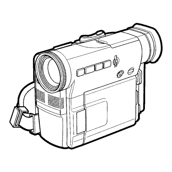
VL-PD3S/H/E VL-PD3S/H/E 2. PART NAMES For details on the use of each control. -
Page 4: Disassembly Of The Set
VL-PD3S/H/E VL-PD3S/H/E 3. DISASSEMBLY OF THE SET Note: Before removing the cabinet, turn off the power supply, and ascertain that the battery have been removed. V/F section · Up the section of V/F, and remove the screw ((D)XiPSF17P03000) · Remove the screws ((D)XiPSF17P03000)(4pcs.) of the bottom (1pc.). - Page 5 VL-PD3S/H/E VL-PD3S/H/E · Turn to a right angle the shaft of the LCD tilt unit section, turn the LCD tilt unit and it is perpendicular to the LCD cabinet. · Remove the fixing screws ((G)XiPSN17P03000)(5pcs.), ((D) XiPSF17P03000)(2pcs.) and LCD cabinet.
-
Page 6: Mechanism Adjustment Jigs And Parts
VL-PD3S/H/E VL-PD3S/H/E 4. MECHANISM ADJUSTMENT JIGS AND PARTS Configuration 1. Name 4-1. Mechanism check adjustment jigs 2. Part No. 3. Code <Note: The entries of list> * Model, Uses Remarks 1. Tension gauge 4N 1. PB-use cassette 1. Dial tension gauge 1. -
Page 7: Inspection And Maintenance Items And Intervals
VL-PD3S/H/E VL-PD3S/H/E 5. INSPECTION AND MAINTENANCE ITEMS AND INTERVALS In order to keep the mechanical section always in good condition, perform the following inspection and maintenance at regular intervals. In addition, after repair, perform the following maintenance items regardless of how long the user has been using the unit. -
Page 8: Mechanical Adjustments And Checks
VL-PD3S/H/E VL-PD3S/H/E 6. MECHANICAL ADJUSTMENTS AND CHECKS The items discussed here relate to general on-site servicing (field servicing). Adjustments and replacements that require sophisticated facilities, jigs and technology are omitted. In addition, in order to maintain the characteristics that the unit has when it is new, not only are inspection and maintenance necessary, but it is absolutely necessary that, for example, the tape not be damaged, and always use jigs for adjustments that require them. - Page 9 VL-PD3S/H/E VL-PD3S/H/E 6-4. Back tension torque check and adjustment in record (playback) mode AC adapter used, with cassette controller assembly Tension roller position (S guide standard) (1) Checking 0 ± 0.3 Set the torque cassette (SD-1015), and make sure in the SP record mode that...
- Page 10 VL-PD3S/H/E VL-PD3S/H/E <REW back tension standard> (If the tension fluctuates, read its center value.) 15 ± mN (1.5 ± gf ) 6-8. Checking of winding Tu reel base ratchet torque DC3V, without cassette controller assembly (Independent Mechanism) (1) Remove the cassette controller assembly, then apply DC3V to the loading motor and put the system into standby mode.
-
Page 11: Tape Running Adjustment
VL-PD3S/H/E VL-PD3S/H/E 7. TAPE RUNNING ADJUSTMENT 7-1. Adjustment locations <Replacement parts> Adjust the height of only · T roller, arm replaced parts with the · Tu guide, arm adjusting jig. · Slide chassis Adjustment procedure 7-2 Running rough Running final... - Page 12 VL-PD3S/H/E VL-PD3S/H/E 7-4. Running rough adjustment (Since this adjustment is performed without cassette controller, put a proper weight so that the cassette does not rise , and make an adjustment.) 1) Su, Tu guide roller height adjustment Entrance side Exit side <Method and description>...
-
Page 13: Mechanical Section Assembly And Parts Replacement (Disassembly And Reassenbly)
VL-PD3S/H/E VL-PD3S/H/E 8. MECHANICAL SECTION ASSEMBLY AND PARTS REPLACEMENT (DISASSEMBLY AND REASSEMBLY) Mechanical section disassembly and reassembly are explained in this section. For removal of the cabinet, etc., refer to 3. DISASSEMBLY OF THE SET. <Precautions> 1. Always replace cut washers that have been removed, for example in parts replacement, with new ones. - Page 14 VL-PD3S/H/E VL-PD3S/H/E (6) STOP mode (5) PLAYBACK (RECORD, FF, VSF) mode The system is in the STOP (Rec Lock in CAMERA mode) The mechanism position for playback, record, FF and fast position; the S and the T pole bases are snap-fitted to the drum feed playback.
- Page 15 VL-PD3S/H/E VL-PD3S/H/E 8-3. How to operate with the circuit board without the cassette controller assembly. In this method, if the procedure is followed incorrectly there is danger of damaging the mechanism and the tape, so except in special cases, such as when measuring the VSR torque, do not perform this procedure. Normally operate this unit with the cassette controller assembly attached.
- Page 16 VL-PD3S/H/E VL-PD3S/H/E 8-5. Reassembly 8-5-1. Reassembly in side of the main chassis. Note) Numbers before part names are given as a guide to the order of assembly. As for greasing/oiling/cleaning places refer to the attached drawings (Grease/Oil application Fig. 1, 2).
- Page 17 VL-PD3S/H/E VL-PD3S/H/E Guide roller assembly (3) Dew FPC cover P SL chassis holder S S pole base assembly (2) Down switch attachment angle Solder-joint assembly Tu pole base assembly Fit, clamping the plate S loading arm assembly Positioning (1) AHC assembly...
- Page 18 VL-PD3S/H/E VL-PD3S/H/E (6) T roller upper flange (6) T roller Ass'y (6) T roller inner (2) T roller upper T arm SPR. flange (6) T roller bottom flange (6) F (2) Tu pole (6) Guide adjustment SPR. (2) T roller bottom...
- Page 19 VL-PD3S/H/E VL-PD3S/H/E GREASE/OIL APPLICATION From rear surface side From rear surface side 303 Pinch control lever 304 Main cam 306 Loading lever 307 S loading arm 312 Intermediate gear angle 308 Tu loading arm Enabled after Oiling Oiling assembling Including groove...
-
Page 20: Adjusting The Electrical Circuits
Chip ID as per Digital Interface IEEE1394 Standard The VL-PD3S/H/E and other models that follow are newly equipped with the digital interface function. The Digital Interface IEEE1394 Standard stipulates that each set with the digital interface function be given its specific ID number. The ID number is written on the E PROM of the set while it is manufactured. - Page 21 VL-PD3S/H/E VL-PD3S/H/E Accordingly, the repair engineer must obtain the new ID number. If you have any question, please contact bolow. ma_waki@toh.sharp.co.jp 3. Enter model number, serial number, company name and FAX, as well as your own name. After confirmation, click OK .
- Page 22 VL-PD3S/H/E VL-PD3S/H/E VL-PD3S/H/E Service jig configuration SC2401...
- Page 23 VL-PD3S/H/E VL-PD3S/H/E VL-PD3S/H/E Specifications of service jigs No. of pins New or Price No. Connection section Connector REF. No. Part cord Continuation code H/A PWB-H/A FPC P306- 80B-B QCNW-1832TAZZ H/A FPC-MAIN2 -SC3301 80B-B CPWBH2876TA01's Unit use POW2-MAIN2 SC901-P1901 90B-B QCNW-1908TAZZ...
- Page 24 VL-PD3S/H/E VL-PD3S/H/E [TEST POINT] (Wiring board diagram: Main2 Side A) (Wiring board diagram: Main1 Side A) TL7403 TL601 TL3333 TL3343 TL2408 TL2410 TL1408 EE level TL3331 TL3314 TL3349 TL2406 TL1407 TL3313 PCO D/A-Y TL3330 TL3345 Frequency character check TL3310 TL2401...
- Page 25 VL-PD3S/H/E VL-PD3S/H/E [Making adjustments] Adjusting the servo system controller and related parts 1. Setting the system codes Replacement of IC703 E PROM requires the following data to be set in this order. [Procedure] Set the unit to the VCR mode and set the data for each address.
- Page 26 VL-PD3S/H/E VL-PD3S/H/E ADJUSTING THE ELECTROMAGNETIC CONVERSION CIRCUIT SYSTEM Note: During the adjustment of the electromagnetic conversion circuit system, keep R3404 out of operation. 1. PLL VCO adjustment Mode VCR ADJ mode Procedure 1) Playback the alignment tape (or a self-recorded tape).
- Page 27 VL-PD3S/H/E VL-PD3S/H/E ADJUSTING THE VIDEO I/O CIRCUIT SYSTEM (Wiring board diagram: Main1 Side A) TL1408 TL1407 PCO D/A-Y PCO D/A-C C1425 R1420 C1442 L1407 TL1408 C1426 R1422 C1409 C1422 C1411 IC4701 L1402 C1424 L1401 C1420 TL1406 TL1008 C1419 TL1013 IC1401...
- Page 28 VL-PD3S/H/E VL-PD3S/H/E ADJUSTING THE LCD CIRCUIT * To make this adjustment, set the backlight switch to the "NORMAL" position. TL1824 (Wiring board diagram: LCD Side A) Common pulse H-position TL1810 Contrast SC800 SC801 SC802 R1855 C5806 L5801 TL818 TL820 TL5802...
- Page 29 VL-PD3S/H/E VL-PD3S/H/E 4. COMMON PULSE adjustment Test point TL1814 Address Mode VCR AV input Procedure 1) Set the data of address 85 at the address 80. 2) Input the white 100% signal as an AV input. 3) Connect the oscilloscope to TL1824, and adjust the pulse width.
- Page 30 VL-PD3S/H/E VL-PD3S/H/E ADJUSTMENT OF VIEW FAR CIRCUIT TL8817 TL8827 TL8824 TL8809 C1714 C1904 R1916 IC1702 TL3408 C1712 TL3367 C1916 C1718 C1903 TL1701 TL3323 Q1902 Q1704 TL8823 C1706 R1710 TL8822 L1904 TL8821 C1723 Q1903 C7703 R1907 R1702 TL8820 C1707 R8836 TL8819...
- Page 31 VL-PD3S/H/E VL-PD3S/H/E 3. VF contrast adjustment Test point TL8811 (VG) Address VCR ADJ 45 Mode VCR AV input Procedure 1) The input signal must be 3-step wave. 2) Connect TL8825 (IC8800 pin 53) to GND. 3) Change the address 41/42 to 00.
- Page 32 VL-PD3S/H/E VL-PD3S/H/E ADJUSTING THE MIC AMP CIRCUIT TL601 (Wiring board diagram: Main1 Side A) EE level Frequency character check (INT MIC R) TL611 TL601 TL603 TL602 P3701 EE level TL603 IC4701 Frequency character check TL3703 TL3702 TL3701 (INT MIC L)
- Page 33 VL-PD3S/H/E VL-PD3S/H/E 9-2. Camera Section Adjustments 9-2-1. Camera section service (1) Camera adjustment is performed after the set has been completed. (2) Subjects, measuring instruments and jigs needed for camera section service and adjustments • Gray scale chart • Frequency counter •...
- Page 34 VL-PD3S/H/E VL-PD3S/H/E 4) Operation flow FF or REW PLAY FF or REW PLAY STOP Address is selected and specified, with the data called. Then the called data are selected and fixed. The operation flows in this sequence. 5) When the adjustment is complete: Press the "CONTINUE"...
- Page 35 VL-PD3S/H/E VL-PD3S/H/E 2) Shifting to the normal operation mode Set the data for the address "00B0" to " FF". This shifts the mode to the normal operation mode. Press the "CONTINUE" key, and the "CAM ADJ" display goes out of the screen, enabling the normal operation.
- Page 36 VL-PD3S/H/E VL-PD3S/H/E 9-2-4. Adjustment procedures Adjustment method Item (1) Auto-focus adjustment Set the unit to the auto-focus function adjustment mode and write data to the address "05FD" one after another. This executed the adjustments automatically. The items to be adjusted are as listed below. Every time an adjustment is made properly, the data "FF"...
- Page 37 VL-PD3S/H/E VL-PD3S/H/E Adjustment method Item (4) Iris AE adjustment (1) Write the data " 00 " to adress "0133". • Measurement terminal: (2) Video output is observed with the oscilloscope in the grey scale standard record state, S terminal luminance signal output the data of address "00B2"...
- Page 38 VL-PD3S/H/E VL-PD3S/H/E Adjustment method Item (1) White balance adjustment is performed repeatedly. (7) White balance adjustment • Measurement terminal: EE output • Address: "0018" INDOOR W/BR "001A" INDOOR W/BR • Measuring instrument: Vector scope • Object: Grey scale • Data variation width: "0000"...
-
Page 39: Useful Tips
VL-PD3S/H/E VL-PD3S/H/E 10. USEFUL TIPS (PROBLEMS DIFFER FROM THOSE FOUND ON VHS OR 8MM DECKS BECAUSE THE SIGNALS ARE DIGITALLY PROCESSED.) Camera (EE mode) Camera (REC mode) VCR (EE mode) VCR (PB mode) Picture fails to appear when tape Picture fails... -
Page 40: Signal Flow Diagrams
VL-PD3S/H/E VL-PD3S/H/E 11. SIGNAL FLOW DIAGRAMS 11-1. EE MODE FLOW (VIDEO) WAVEFORM DIAGRAM (DURING COLOUR BAR RECORDING) IC4453 81pin Y/YC Output ADIN CH1=500mV 20µs/d DC P*10 8 11 CAMERA IC201 IC4453 112pin ZYP3 Input CH1=1V 5ms/d 82 85 92 94... - Page 41 VL-PD3S/H/E VL-PD3S/H/E WAVEFORM DIAGRAM 11-3.FLOW IN PB MODE (VIDEO) (DURING COLOUR BAR PLAYBACK) HEAD AMP PB_DATA IC3404 5pin Input IC3402 4pin PBDATA Input B TO B SC3301 PB_DATA IC3402 IC3403 IC491 IC431 8pin VDATA3 Output IC3401 54pin Input 2 1 2 1...
- Page 42 VL-PD3S/H/E VL-PD3S/H/E 11-5.FLOW IN PB MODE (AUDIO) WAVEFORM DIAGRAM (1.6 kHz SINE WAVE) From IC3403 IC431 21 ADATA3 Output same as in Video PB system IC431 TRANSPORT ADATA 68 69 71 77 78 IC1650 DODAT ADC/DAC IC1601 15 DODAT Input...
-
Page 43: Block Diagrams
VL-PD3S/H/E VL-PD3S/H/E 12. BLOCK DIAGRAMS 12-1. SYSTEM BLOCK DIAGRAM 11-4 12-1... - Page 44 VL-PD3S/H/E VL-PD3S/H/E 12-2. CAMERA SECTION BLOCK DIAGRAM 11-5 12-2...
- Page 45 VL-PD3S/H/E VL-PD3S/H/E 12-3. PPW SECTION BLOCK DIAGRAM 11-6 12-3...
- Page 46 VL-PD3S/H/E VL-PD3S/H/E 12-4. CODEC SECTION BLOCK DIAGRAM 12-4 11-7...
- Page 47 VL-PD3S/H/E VL-PD3S/H/E 12-5. AUDIO/DIGITAL OUTPUT SECTION BLOCK DIAGRAM 11-8 12-5...
- Page 48 VL-PD3S/H/E VL-PD3S/H/E 12-6. CAMERA CIRCUIT BLOCK DIAGRAM 11-9 12-6...
- Page 49 VL-PD3S/H/E VL-PD3S/H/E - M E M O - 12-7 11-10...
-
Page 50: Schematic Diagrams
VL-PD3S/H/E 13. SCHEMATIC DIAGRAMS 13-1. OVERALL SCHEMATIC DIAGRAM LOCATION MAP: (1/4) 13-1... - Page 51 VL-PD3S/H/E LOCATION MAP: (2/4) 13-2...
- Page 52 VL-PD3S/H/E LOCATION MAP: (3/4) 13-3...
- Page 53 VL-PD3S/H/E LOCATION MAP: (4/4) 13-4...
- Page 54 VL-PD3S/H/E 13-2. AUDIO I/O CIRCUIT SCHEMATIC DIAGRAM 13-5...
- Page 55 VL-PD3S/H/E 13-6...
- Page 56 VL-PD3S/H/E 13-3. CONN1 CIRCUIT SCHEMATIC DIAGRAM 13-7...
- Page 57 VL-PD3S/H/E 13-8...
- Page 58 VL-PD3S/H/E 13-4. DAC CIRCUIT SCHEMATIC DIAGRAM 13-9...
- Page 59 VL-PD3S/H/E 13-10...
- Page 60 VL-PD3S/H/E 13-5. SYSTEM CONTROL CIRCUIT SCHEMATIC DIAGRAM 13-11...
- Page 61 VL-PD3S/H/E 13-12...
- Page 62 VL-PD3S/H/E 13-6. ADC CIRCUIT SCHEMATIC DIAGRAM 13-13...
- Page 63 VL-PD3S/H/E 13-14...
- Page 64 VL-PD3S/H/E 13-7. CAM-DSP CIRCUIT SCHEMATIC DIAGRAM 13-15...
- Page 65 VL-PD3S/H/E 13-16...
- Page 66 VL-PD3S/H/E 13-8. ZOOM CIRCUIT SCHEMATIC DIAGRAM LOCATION MAP: (1/4) 13-17...
- Page 67 VL-PD3S/H/E LOCATION MAP: (2/4) 13-18...
- Page 68 VL-PD3S/H/E LOCATION MAP: (3/4) 13-19...
- Page 69 VL-PD3S/H/E LOCATION MAP: (4/4) 13-20...
- Page 70 VL-PD3S/H/E 13-9. CODEC CIRCUIT SCHEMATIC DIAGRAM LOCATION MAP: (1/4) 13-21...
- Page 71 VL-PD3S/H/E LOCATION MAP: (2/4) 13-22...
- Page 72 VL-PD3S/H/E LOCATION MAP: (3/4) 13-23...
- Page 73 VL-PD3S/H/E LOCATION MAP: (4/4) 13-24...
- Page 74 VL-PD3S/H/E 13-10. PPW CIRCUIT SCHEMATIC DIAGRAM 13-25...
- Page 75 VL-PD3S/H/E 13-26...
- Page 76 VL-PD3S/H/E 13-11. VIDEO I/O CIRCUIT SCHEMATIC DIAGRAM 13-27...
- Page 77 VL-PD3S/H/E 13-28...
- Page 78 VL-PD3S/H/E 13-12. SVART LENS MICON CIRCUIT SCHEMATIC DIAGRAM 13-29...
- Page 79 VL-PD3S/H/E TO REM CON UNIT TO POW SW 13-30...
- Page 80 VL-PD3S/H/E 13-13. EQ/PLL CIRCUIT SCHEMATIC DIAGRAM 13-31...
- Page 81 VL-PD3S/H/E 13-32...
- Page 82 VL-PD3S/H/E 13-14. CONNECTION(B-B) CIRCUIT SCHEMATIC DIAGRAM 13-33...
- Page 83 VL-PD3S/H/E 13-34...
- Page 84 VL-PD3S/H/E 13-15. CONN2 CIRCUIT SCHEMATIC DIAGRAM 13-35...
- Page 85 VL-PD3S/H/E 13-36...
- Page 86 VL-PD3S/H/E 13-16. MECHACON CIRCUIT SCHEMATIC DIAGRAM 13-37...
- Page 87 VL-PD3S/H/E 13-38...
- Page 88 VL-PD3S/H/E 13-17. MOTOR DRIVE CIRCUIT SCHEMATIC DIAGRAM 13-39...
- Page 89 VL-PD3S/H/E 13-40...
- Page 90 VL-PD3S/H/E 13-18. PCM CIRCUIT SCHEMATIC DIAGRAM 13-41...
- Page 91 VL-PD3S/H/E 13-42...
- Page 92 VL-PD3S/H/E 13-19. POWER1 CIRCUIT SCHEMATIC DIAGRAM LOCATION MAP: (1/4) 13-43...
- Page 93 VL-PD3S/H/E LOCATION MAP: (2/4) 13-44...
- Page 94 VL-PD3S/H/E LOCATION MAP: (3/4) 13-45...
- Page 95 VL-PD3S/H/E LOCATION MAP: (4/4) 13-46...
- Page 96 VL-PD3S/H/E 13-20. TRANSPORT CIRCUIT SCHEMATIC DIAGRAM LOCATION MAP: (1/4) 13-47...
- Page 97 VL-PD3S/H/E LOCATION MAP: (2/4) 13-48...
- Page 98 VL-PD3S/H/E LOCATION MAP: (3/4) 13-49...
- Page 99 VL-PD3S/H/E LOCATION MAP: (4/4) 13-50...
- Page 100 VL-PD3S/H/E 13-21. DIGITAL I/F CIRCUIT SCHEMATIC DIAGRAM 13-51...
- Page 101 VL-PD3S/H/E 13-52...
- Page 102 VL-PD3S/H/E 13-22. V/F CIRCUIT SCHEMATIC DIAGRAM 13-53...
- Page 103 VL-PD3S/H/E 13-54...
- Page 104 VL-PD3S/H/E 13-23. TG CIRCUIT SCHEMATIC DIAGRAM 13-55...
- Page 105 VL-PD3S/H/E 13-56...
- Page 106 VL-PD3S/H/E 13-24. CCD CIRCUIT SCHEMATIC DIAGRAM 13-57...
- Page 107 VL-PD3S/H/E 13-58...
- Page 108 VL-PD3S/H/E 13-25. LENS DRIVE CIRCUIT SCHEMATIC DIAGRAM 13-59...
- Page 109 VL-PD3S/H/E 13-60...
- Page 110 VL-PD3S/H/E 13-26. CDS CIRCUIT SCHEMATIC DIAGRAM 13-61...
- Page 111 VL-PD3S/H/E 13-62...
- Page 112 VL-PD3S/H/E 13-27. LENS CONNECTION CIRCUIT SCHEMATIC DIAGRAM 13-63...
- Page 113 VL-PD3S/H/E 13-64...
- Page 114 VL-PD3S/H/E 13-28. POWER2 CIRCUIT SCHEMATIC DIAGRAM å AND SHADED COMPONENTS=SAFETY RELATED PARTS LOCATION MAP: (1/4) 13-65...
- Page 115 VL-PD3S/H/E MAIN1 P.W.B. Wiring Side SIDE B 15-4...
- Page 116 VL-PD3S/H/E MAIN2 P.W.B. Component Side SIDE A TL7403 TL3333 TL3343 TL2408 TL2410 TL3331 TL3314 TL3349 TL2406 TL3313 TL3330 TL3345 TL3310 TL2401 TL2403 TL3366 R2404 TL3329 TL7405 TL7402 TL7404 TL2402 TL3364 TL7401 TL3306 TL3305 TL3326 TL3332 C7401 FB7401 TL3327 TL2404 TL2409...
- Page 117 VL-PD3S/H/E MAIN2 P.W.B. Wiring Side SIDE A 15-6...
- Page 118 VL-PD3S/H/E MAIN2 P.W.B. Component Side SIDE B J2401 L2401 FB2403 R2403 C1658 R7428 FL1650 R7419 FB2402 C7419 R7429 R7422 R7414 R1658 R7415 C1615 C1661 C1656 R1651 C1611 R7413 C1609 R7411 C1614 C1617 C1652 C1654 R7409 R7410 R1667 R1662 C7408 C7410...
- Page 119 VL-PD3S/H/E MAIN2 P.W.B. Wiring Side SIDE B 15-8...
- Page 120 VL-PD3S/H/E CAMERA HEAD P.W.B. Component Side SIDE A TL546 TL101 R551 IC551 TL102 R501 TL510 TL537 TL511 TL514 C501 C559 TL536 R109 C109 L551 R110 C565 C108 TL23 TL10 TL14 TL16 TL11 TL12 IC12 R107 R101 C101 TL8 TL7 TL6...
- Page 121 VL-PD3S/H/E Component Side SIDE B TL540 TL520 TL562 C563 R582 R553 TL561 TL545 TL563 R581 IC13 C552 C556 R568 R583 R552 TL560 TL556 TL513 TL521 TL533 TL508 TL559 C572 TL527 TL543 R573 R569 R584 R572 TL528 TL526 R574 C570 TL539...
- Page 122 VL-PD3S/H/E POWER P.W.B. Component Side SIDE A R979 C921 R936 C919 C917 C908 R935 C916 C920 R907 C938 IC900 R901 R917 C902 R916 R921 R926 C910 R927 R913 C913 R931 R986 R920 C905 C909 R929 R987 R911 R971 C901 R910...
- Page 123 VL-PD3S/H/E POWER P.W.B. Wiring Side SIDE A 15-12...
- Page 124 VL-PD3S/H/E POWER P.W.B. Component Side SIDE B R9909 C9909 R9920 R9907 R9929 R9933 C9902 C9917 R9913 R9917 R9910 R9931 R9924 R9935 C9915 R9922 C9919 C9923 C9907 C9950 R9950 C9927 R9906 IC9900 R9905 R9942 R9940 C9903 R9937 R9919 C9920 R9925 R9928...
- Page 125 VL-PD3S/H/E POWER P.W.B. Wiring Side SIDE B 15-14...
- Page 126 VL-PD3S/H/E LCD P.W.B. Component Side SIDE A SC801 SC802 SC800 R1855 L5801 C5806 TL818 TL820 TL5802 TL5804 TL1825 TL825 TL824 TL5803 TL5801 TL827 TL828 TL1824 TL835 TL836 TL837 TL838 TL829 TL830 TL831 TL814 TL815 C1827 TL822 C5800 TL817 TL819 TL826...
- Page 127 VL-PD3S/H/E HEAD AMP P.W.B. Component Side SIDE A Wiring Side SIDE A Wiring Side SIDE B 15-16...
- Page 128 VL-PD3S/H/E - M E M O - 15-17...
-
Page 129: Printed Wiring Board Assemblies
PRINTED WIRING BOARD ASSEMBLIES Q4441 VS2PC4617R/-1 2PC4617R (NOT REPLACEMENT ITEM) Q4442 VSXP6401///-1 XP6401 Q4461 VSUPUMZ1///-1 UPUMZ1 Q4462 VSUPUMZ1///-1 UPUMZ1 DUNTK2871PM02 MAIN1 PWB Unit(VL-PD3S) – Q4463 VSUPUMZ1///-1 UPUMZ1 DUNTK2871PM03 MAIN1 PWB Unit(VL-PD3H) – Q4464 VSUPUMZ1///-1 UPUMZ1 DUNTK2871PM04 MAIN1 PWB Unit – Q4465 VSUPUMZ1///-1 UPUMZ1... - Page 130 VL-PD3S/H/E VL-PD3S/H/E Ref. No. Part No. Description Code Ref. No. Part No. Description Code L4401 VPD9M150K1R3N Peaking 15µH C412 VCKYCZ1HF103Z 0.01 50V Ceramic L4402 VPD9M220K2R0N Peaking 22µH C413 VCKYCZ1HF103Z 0.01 50V Ceramic L4403 VPM6N100MR75N Peaking 10µH C414 VCKYCZ1HF103Z 0.01 50V Ceramic...
- Page 131 VL-PD3S/H/E VL-PD3S/H/E Ref. No. Part No. Description Code Ref. No. Part No. Description Code C711 VCKYCZ1HB102K 1000p 50V Ceramic C4429 VCKYCZ1HF103Z 0.01 50V Ceramic C712 VCKYCZ1HB102K 1000p 50V Ceramic C4435 VCKYCZ1HF103Z 0.01 50V Ceramic C713 VCKYCZ1AF104Z 10V Ceramic C4436 VCSAPR0JJ106M 6.3V Tantalum...
- Page 132 VL-PD3S/H/E VL-PD3S/H/E Ref. No. Part No. Description Code Ref. No. Part No. Description Code R622 VRS-CZ1JF103J 10k 1/16W Metal Oxide R1418 VRS-CZ1JF750J 1/16W Metal Oxide R623 VRS-CZ1JF222J 2.2k 1/16W Metal Oxide R1419 VRS-CZ1JF000J 1/16W Metal Oxide R624 VRS-CZ1JF223J 22k 1/16W Metal Oxide...
- Page 133 Part No. Description Code Ref. No. Part No. Description Code R4422 VRS-CZ1JF472J 4.7k 1/16W Metal Oxide DUNTK2872PM02 MAIN2 PWB UNIT(VL-PD3S) R4426 VRS-CZ1JF103D 10k 1/16W Metal Oxide DUNTK2872PM03 MAIN2 PWB UNIT(VL-PD3H) R4430 VRS-CZ1JF102J 1/16W Metal Oxide DUNTK2872PM04 MAIN2 PWB UNIT(VL-PD3E/EW/EX) R4431 VRS-CZ1JF472J 4.7k 1/16W Metal Oxide...
- Page 134 VL-PD3S/H/E VL-PD3S/H/E Ref. No. Part No. Description Code Ref. No. Part No. Description Code COILS C1612 VCKYCZ1AF104Z 10V Ceramic C1613 VCSAPR1AJ475M 10V Tantalum FL1650 RCiLZ0283TAZZ Coil C1614 VCKYCZ1HB222K 2200p 50V Ceramic FL2401 RCiLF0391TAZZ Coil C1615 VCKYCZ1AF104Z 10V Ceramic FL3401 RCiLF0376TAZZ...
- Page 135 VL-PD3S/H/E VL-PD3S/H/E Ref. No. Part No. Description Code Ref. No. Part No. Description Code C2401 VCKYCZ1HB102K 1000p 50V Ceramic C7406 VCCCCZ1HH150J 50V Ceramic C2402 VCKYCZ1HB102K 1000p 50V Ceramic C7407 VCCCCZ1HH150J 50V Ceramic C3401 VCCCCZ1HH220J 50V Ceramic C7408 VCCCCZ1HH101J 100p 50V Ceramic...
- Page 136 VL-PD3S/H/E VL-PD3S/H/E Ref. No. Part No. Description Code Ref. No. Part No. Description Code R440 VRS-CZ1JF000J 1/16W Metal Oxide R1920 VRS-CZ1JF105J 1/16W Metal Oxide R441 VRS-CZ1JF103J 10k 1/16W Metal Oxide R1921 VRS-CZ1JF104J 100k 1/16W Metal Oxide R442 VRS-CZ1JF102J 1/16W Metal Oxide...
- Page 137 VL-PD3S/H/E VL-PD3S/H/E Ref. No. Part No. Description Code Ref. No. Part No. Description Code R8808 VRK-SB1FF222J 2.2k 0.0315W R3455 VRS-CZ1JF000J 1/16W Metal Oxide Metal Composition R3458 VRS-CZ1JF121J 120 1/16W Metal Oxide R8812 VRS-CZ1JF103J 10k 1/16W Metal Oxide R3463 VRS-CZ1JF112J 1.1k 1/16W Metal Oxide...
- Page 138 VL-PD3S/H/E VL-PD3S/H/E Ref. No. Part No. Description Code Ref. No. Part No. Description Code FILTER AND COILS VRS-CZ1JF105J 1/16W Metal Oxide VRS-CZ1JF105J 1/16W Metal Oxide PFiLW0076TAZZ Filter VRS-CZ1JF000J 1/16W Metal Oxide VPAWM100K1R5N Peaking 10µH VRS-CZ1JF104J 100k 1/16W Metal Oxide L101 VPAWM100K1R5N Peaking 10µH...
- Page 139 VL-PD3S/H/E VL-PD3S/H/E Ref. No. Part No. Description Code Ref. No. Part No. Description Code C903 VCKYCZ1AF104Z 10V Ceramic DUNTK2874PM01 POWER PWB UNIT C904 VCKYCZ1AB104K 10V Ceramic C905 VCKYCZ1AB104K 10V Ceramic C906 VCKYCZ1AB104K 10V Ceramic INTEGRATED CIRCUITS C907 VCCCCZ1HH101J 100p 50V Ceramic å...
- Page 140 VL-PD3S/H/E VL-PD3S/H/E Ref. No. Part No. Description Code Ref. No. Part No. Description Code C9920 VCKYCZ1HB102K 1000p 50V Ceramic R9914 VRS-CZ1JF103D 10k 1/16W Metal Oxide C9921 VCKYCZ1HB102K 1000p 50V Ceramic R9915 VRS-CZ1JF133D 13k 1/16W Metal Oxide C9922 VCKYCZ1HB102K 1000p 50V Ceramic...
- Page 141 VL-PD3S/H/E VL-PD3S/H/E Ref. No. Part No. Description Code Ref. No. Part No. Description Code CAPACITORS RESISTORS C800 VCSATE1CJ226M 16V Tantalum R800 VRS-CZ1JF000J 1/16W Metal Oxide C803 VCKYCZ1AF104Z 10V Ceramic R801 VRS-CZ1JF304D 300k 1/16W Metal Oxide C804 VCKYCZ1AF104Z 10V Ceramic R802...
- Page 142 VL-PD3S/H/E VL-PD3S/H/E Ref. No. Part No. Description Code Ref. No. Part No. Description Code R1840 VRS-CZ1JF393J 39k 1/16W Metal Oxide C320 VCKYCZ1AF104Z 10V Ceramic R1841 VRS-CZ1JF474J 470k 1/16W Metal Oxide C321 VCKYCZ1HB102K 1000p 50V Ceramic R1842 VRS-CZ1JF104J 100k 1/16W Metal Oxide...
- Page 143 VL-PD3S/H/E VL-PD3S/H/E Ref. No. Part No. Description Code Ref. No. Part No. Description Code MSPRT0418GEFJ T Arm SPR. MECHANISM PARTS MSPRD0178GEFJ Tu Guide Arm SPR. MSPRD0179GEFJ Pinch Lever Return SPR. DMECV0063GE08 Mechanism Ass'y(PD3H/E) – MSPRD0180GEFJ S Pressure SPR. DMECV0063GE09 Mechanism Ass'y(PD3S) –...
- Page 144 VL-PD3S/H/E VL-PD3S/H/E Ref. No. Part No. Description Code Ref. No. Part No. Description Code TLABZ0474TAZZ Special Merit Label A CABINET PARTS LIST DCOVA1601TAK1 K.S. Front Cover(PD3S/H) BB DCOVA1601TAK2 K.S. Front Cover(PD3E) 5-1-2 GCOVA1590TAZZ R/C Catch Light Cover DCABA6201TAK2 K.S. Cabinet Ass'y...
- Page 145 CCD Sensor SPAKA6308TAZZ Packing Case – LANGK0437TAFW CCD Cover Panel SPAKA6306TAZZ Packing Upper – PSLDM3333TAMS Shield Case A SPAKA6307TAZZ Packing Bottom(VL-PD3S) – DUNTK2873QA02 Camera Head PWB Unit – SPAKF0262TAZZ Packing – LX-HZ0073TAFD Screw SPAKP6108TAZZ Side Pad XiPSN17P02000 Screw (1.7 x 2)
- Page 146 VL-PD3S/H/E VL-PD3S/H/E MECHANISM CHASSIS EXPLODED VIEW Ref. No. Part No. Description Code Ref. No. Part No. Description Code 411~ 1pc. 411~ 1pc. 334 341 402 470 16-18...
- Page 147 VL-PD3S/H/E VL-PD3S/H/E CABINET EXPLODED VIEW Ref. No. Part No. Description Code Ref. No. Part No. Description Code 1-1-9 1-12 1-1-11 5-1-11 1-11 5-10 6-1-2 5-1-9 6-1-7 6-1-9 6-1-5 5-1-5 6-1-3 5-1-6 5-1-12 6-1-12 6-1-14 1-13 5-1-10 6-1-8 5-1-4 5-1-8 6-1-11...
- Page 148 VL-PD3S/H/E VL-PD3S/H/E CASSETTE CONTROL EXPLOOD VIEW Ref. No. Part No. Description Code Ref. No. Part No. Description Code CAMERA UNIT EXPLOOD VIEW Face the slope part toward the lens side. CCD side Lens side Face the thinner part toward the lens side.
- Page 149 VL-PD3S/H/E VL-PD3S/H/E LENS UNIT EXPLOOD VIEW Ref. No. Part No. Description Code Ref. No. Part No. Description Code 16-21...
- Page 150 VL-PD3S/H/E VL-PD3S/H/E VL-PD3S/H/E SERVICE JIG SPECIFICATIONS Ref. No. Part No. Description Code Ref. No. Part No. Description Code 1-1. Adjusting jigs for checking the mechanism Name New part Type number, Application Part code Code PB-use cassette torque meter 10g·cm/15g·cm 9DASD-1015...
-
Page 151: Packing Of The Set
VL-PD3S/H/E VL-PD3S/H/E 17. PACKING OF THE SET Ref. No. Part No. Description Code Ref. No. Part No. Description Code QCNW-1831TAZZ QCNW-1910TAZZ UBATi0053TAZZ UADP-0296TAZZ CCNW-1912TA01 QCNW-1903TAZZ (PD3E/EW) (PD3S/H/EX) Battery Pack AC Adapter/ (PD3S/H/EX) (PD3E/EW) S-Video/Video/Audio S-Video/Video/Audio Battery Charger DC Cable DC Cable... - Page 152 Code Ref. No. Part No. Description Code COPYRIGHT C 1999 BY SHARP CORPORATION ALL RIGHTS RESERVED. No part of this publication may be reproduced, stored in a retrieval system, or transmitted in any form or by any means, electronic, mechanical, photocopying, recording, or otherwise, without prior written permission of the publisher.
Need help?
Do you have a question about the VL-PD3S and is the answer not in the manual?
Questions and answers