Table of Contents
Advertisement
Quick Links
Advertisement
Table of Contents
Troubleshooting

Related Manuals for Panasonic SV-MP720VSG


Summary of Contents for Panasonic SV-MP720VSG
- Page 1 TD0508048C3 Digital Audio Player SV-MP720VSG / SV-MP730VSG Colour (K)....Black Type (S)....Silver Type (W)....White Type SPECIFICATIONS Specifications PDF created with pdfFactory Pro trial version www.pdffactory.com...
- Page 2 SV-MP720V: 512 MB Memory size: SV-MP730V: 1 GB MP3; 32 kHz, 44.1 kHz,and 48 Supported sampling frequency: WMA; 8 kHz to 44.1 kHz MP3; 8 kbps to 320 kbps (128 Supported bit-rates: kbps is recommend) WMA; 32 kbps to 192 kbps (96 kbps is recommend) Stereo, 2 channels (MUSIC, FM No.
- Page 3 1. Accessories - Stereo earphones (L0BAB0000188) ............. 1pc. - USB Cable (K1HA05AD0003)............. 1pc. - Neck Strap (RFAT0006-Q) ..............1pc. - CD-ROM Driver (RFET0004) ..............1pc. - AC Adaptor (N0JZCD000003) ...............1pc. PDF created with pdfFactory Pro trial version www.pdffactory.com...
- Page 4 - Battery Ass’y (ZBRP-BP65HE)..............1pc. - Battery Case (RFCT0005-H) ............1pc. 2. Supply of Rechargeable Battery as Replacement Parts - Please take note of the following points relating to Carrying Case to be used for protection of Rechargeable Battery from shorting. Replacement Parts: - Rechargeable Battery (ZBRP-BP65HE) to be supplied will be provided with Carrying Case (RFCT0005-H).
- Page 5 3. Caution in Use of Rechargeable Battery - Take Rechargeable Battery out of Carrying Case and use iy. Be sure to carry Rechargeable Battery in this Carrying Case. If not, may either head or ignite by shorting with a metal. 4.
- Page 6 5.2. Removal of the front cabinet 5.3. Removal of the memory P.C.B. 5.4. Removal of the main P.C.B. PDF created with pdfFactory Pro trial version www.pdffactory.com...
- Page 7 5.5. Removal of the battery terminal. 5.6. Removal of the LCD Ass’y PDF created with pdfFactory Pro trial version www.pdffactory.com...
- Page 8 5.7. Removal of the LCD Piece 5.8. Removal of the mode button and hold knob PDF created with pdfFactory Pro trial version www.pdffactory.com...
- Page 9 5.9. Removal of the USB fix piece and USB cover 5.10. Removal of the REC button 5.11. Removal of the tuner P.C.B. and MIC ass’y PDF created with pdfFactory Pro trial version www.pdffactory.com...
- Page 10 6. Instructions for Repair Service 7. Service Position PDF created with pdfFactory Pro trial version www.pdffactory.com...
-
Page 11: Service Mode
8. Service Mode 8.1. Checking Procedures for IC3 C2HBZG000008 PDF created with pdfFactory Pro trial version www.pdffactory.com... - Page 12 8.2. Checking Procedures for Font table PDF created with pdfFactory Pro trial version www.pdffactory.com...
-
Page 13: Service Precautions
9. Service Precautions 9.1. Install and Copy the software (DFU,firmware,font table) After replacing the main PCB and DSP IC (main CPU),reinstall DFU and firmware,and copy font table again. 9.2. Please contact to the service organization of the belonging for the acquisition of data and obtain the software. PDF created with pdfFactory Pro trial version www.pdffactory.com... - Page 14 PDF created with pdfFactory Pro trial version www.pdffactory.com...
- Page 15 PDF created with pdfFactory Pro trial version www.pdffactory.com...
-
Page 16: Troubleshooting
10. Troubleshooting - What to prepare - A PC that has the exclusive application software (Windows Media Player V9.0) installed. Be sure to check for normal operation of the PC. If other application software is installed in the PC, be sure that this software does not affect the operation of the Windows Media Player V9.0. -
Page 17: Troubleshooting Guide
- When a user’s product is taken in for service, be sure to obtain not only the player and USB reader/writer. Also, try to obtain as much information as possible on the operational environmentofthe user’s PC. <PC’s operational environment> Product name, model number, name of CPU, operation clock, RAM capacity, HD capacity, names of installed software, use of USB hub, and any equipment connected with USB simultaneously. - Page 18 - Before repairing the unit, make the below check. - No operation: - The HOLD function is on. - The rechargeable battery may be depleted. - The power supply switches off: - The SLEEP TIME function is on. - Play time is short after recharging: - This may occur the first time you recharge the battery or if you haven’t used them for a long time.Play time should be restored after a few recharges.
- Page 19 - After downloading music data from the PC,remove the USB cable and turn on the unit.”wait...” appers on the unit’s display while the music data is read. Depending on the number of recorded tracks and folders, the length of time “wait...” is displayed differs. 120 tracks .
- Page 20 : FM RF signal line / : Audio signal line / : Mp3 signal line / : REC signal line / - Important safety notice: Components identified by mark have special characteristics important for safety. Furthermore, special parts which have purposes of fire-retardant (resistors), high-quality sound (capacitors), low-noise (resistors), etc.
- Page 21 18. Packaging PDF created with pdfFactory Pro trial version www.pdffactory.com...
-
Page 22: Replacement Parts List
19. Replacement Parts List Notes: - Important safety notice: Components identified by mark have special characteristics important for safety. Furthermore, special parts which have purposes of fire-retardant (resistors), high-quality sound (capacitors), low-noise (resistors), PDF created with pdfFactory Pro trial version www.pdffactory.com... - Page 23 etc. are used. When replacing any of components, be sure to use only manufactures specified parts shown in the parts list. 1. (T) Indicates parts that are supplied PTW 2. The reference number SA represent the grease tool usea for unit. 3.
- Page 24 Ref. No. Part No. Part Name & Description Remarks RSCT0041 METAL DOME ZA5MP500VGKS LCD PREPARE ASSY K18-1 L5DZBDB00001 LCD WITH FPC (30 Pin) K18-2 L5GZAXZ00001 EL BOARD K18-3 RMNT0098-1 LCD ANGLE RMZT0079 PCB SHEET(UP PCB) RMZT0078 PCB SHEET(MAIN PCB) K21 [MP720V] RQLTA0391B-1 NAME PLATE (Black) RQLTA0391A-1...
- Page 25 C0CBCAC00288 PDF created with pdfFactory Pro trial version www.pdffactory.com...
- Page 26 Ref. No. Part No. Part Name & Description Remarks C0EBC0000204 1.6V RESET IC (4P) IC10 C0CBCAC00288 IC301 C1BB00000934 D-SOUND IC 2SA1774STL TRANSISTOR B1ADMD000012 TRANSISTOR UMX1NTN TRANSISTOR (DIGITAL) B1CFMC000005 B1MBACA00011 FET ARRAY Q302 UN9210JTX TRANSISTOR B0CCAA000001 LOW-VOLTAGE VARIABLE CAP B0CCAA000001 LOW-VOLTAGE VARIABLE CAP MA3J14700L DIODE B0JDDB000002...
- Page 27 Ref. No. Part No. Part Name & Description Remarks L302 J0JBC0000044 CHIP COIL L303 G1C101MA0072 PEAKING COIL L304 G1C101MA0072 PEAKING COIL L305 G1C101MA0099 PEAKING COIL L306 G1C101MA0099 PEAKING COIL IC PROCTECTOR ICP1 K5H5012A0025 PROTECTOR ICP2 K5H5012A0025 PROTECTOR SWITCHES K0H1BB000068 SWITCH K0H1BB000068 SWITCH K0D112B00067...
- Page 28 Ref. No. Part No. Part Name & Description Remarks D0GA104JA020 CHIP RESISTOR D0GA104JA020 CHIP RESISTOR D0GA100JA020 CHIP RESISTOR D0GAR00JA020 CHIP RESISTOR D0GA472JA020 CHIP RESISTOR D0GA563JA020 CHIP RESISTOR D0GA102JA020 CHIP RESISTOR D0GA222JA020 CHIP RESISTOR D0GA104JA020 CHIP RESISTOR D0GA472JA020 CHIP RESISTOR D0GA472JA020 CHIP RESISTOR D0GA184JA020 CHIP RESISTOR...
- Page 29 Ref. No. Part No. Part Name & Description Remarks ECUENC333KBQ CHIP CAPACITOR F1G1C223A004 CHIP CAPACITOR F1G1C223A004 CHIP CAPACITOR ECUVNA105ZFV CHIP CAPACITOR ECUENC333KBQ CHIP CAPACITOR ECUE0J224KBQ CHIP CAPACITOR ECUE0J224KBQ CHIP CAPACITOR F3G0G1070001 TANTALUM CAP. ECUE1H100DCQ CHIP CAPACITOR F1G1C223A004 CHIP CAPACITOR ECUE1H102KBQ CHIP CAPACITOR F1G1C223A004 CHIP CAPACITOR...
- Page 30 Ref. No. Part No. Part Name & Description Remarks F1G0J4740002 CHIP CAPACITOR PSLB30G107M TANTALUM CAP. K105BJ104KVC CHIP CAPACITOR F1G1C103A004 CHIP CAPACITOR F3E0G226A002 TANTALUM CAP. C100 ECUVNA105ZFV CHIP CAPACITOR C101 K105BJ104KVC CHIP CAPACITOR C103 ECUE1H391KBQ CHIP CAPACITOR C104 K105BJ104KVC CHIP CAPACITOR C105 ECUE1H331KBQ CHIP CAPACITOR...
-
Page 31: Location Of Controls
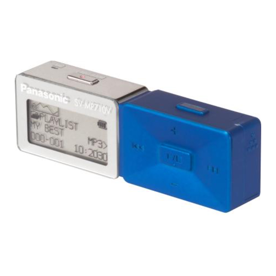
Location of Controls Microphone REC/STOP Skip/search DMODE Volume Battery lid Turn on, off (Press and hold)/ Display HOLD Play/Stop Example:MUSIC switch USB port Earphones jack (3.5 mm stereo) Rechargeable battery (included) Charge before initial use Insert the Charge the battery. rechargeable battery. - Page 32 TUNER P.C.B. (SIDE :A) TUNER P.C.B. (SIDE :B) HEADPHONE JACK JK301 C107 BATTERY TERMINAL( ) MAIN P.C.B. (SIDE :A) MEMORY P.C.B. (SIDE :B) MEMORY P.C.B. (SIDE :A) PLAY/STOP VOL+ MODE C103 MAIN P.C.B.(CN1) Note: This printed circuit board diagram may be modified at any time with the development of new technology.
-
Page 33: Main P.c.b. (Side :A)
MAIN P.C.B. (SIDE :A) MAIN P.C.B. (SIDE :B) MEMORY P.C.B. (CN5) ICP1 C204 C201 C105 HOLD IC10 R202 Jumper Wire C306 C305 R308 C113 C308 L305 R307 1 2 3 C126 C104 C127 C116 C304 C303 Q302 C205 R303 C313 C206 C315 R204... -
Page 34: Tuner Circuit
TUNER CIRCUIT Schematic diagram-1 TP47 TP48 C18 K0.22 K0.22 1.52 0.70 0.69 1.88 1.88 1.44 C23 K0.001 N.C. N.C. K0.022 0.54 LGAIN PILFIL 1.35 AGND PHASEFIL TP43 K0.022 2.59 VCCD XTAL2 13MHz K0.022 D10P 1.05 1.62 RFI 1 XTAL1 C1BB00000997 0.02 K100P FM TUNER... -
Page 35: Memory Circuit
MEMORY CIRCUIT Schematic diagram-2 B0JDDB000002 PLAY MA3J14700L 0.68 0.68 MA2Z74800L 2SA1774STL 1.04 CHARGEABLE 0.69 1.05 VOL+ 0.69 B1ADMD000012 K1KA30A00216 CHARGEABLE MODE 1.2 0 C3FBVC000001..512MB C3FBVC000002..1GB FLASH MEMORY N.C N.C N.C N.C N.C N.C R/B N.C N.C N.C N.C ALE WE WP N.C N.C N.C N.C N.C 2.97 2.94 0 SV-MP720V/MP730V(SG) CIRCUIT DIAGRAM... -
Page 36: Main Circuit
MAIN CIRCUIT Schematic diagram-3 S.S.G F=87.5MHz Mod=30% Mod f=400Hz 233.0mV P-P L201 L202 ICP2 V18 U18 J14 0 BATTERY IN 1.2V J5 0 100K TP10 K1KB24A00044 ICP1 BATTERY TP12 (1.2V) IC10 C0CBCAC00288 REGULATOR 2.8V 2.8V 3.02 VOUT 3.02 1.42 VOUT UMX1NTN Chargeable C0EBC0000204... - Page 37 MAIN CIRCUIT Schematic diagram-4 1.8V CN3 USB CON. K1FB108E0007 A B C D E F G H I J K L U16 U15 T16 R16 R17 P16 U14 T17 U17 T15 J17 V16 V11 H1 A6 A15 A7 A16 H18 F1 J18 V14 V5 E1 F3 C1 C3 D2 D1 D3 E2 E3 F2 G2 V18 U18...
- Page 38 MAIN CIRCUIT Schematic diagram-5 K1MN30B00124 LCD CON. /CS1 /RES WR (R/W) RD(E) C57 Z1.0 VOUT C90 Z1.0 CAP3+ E3 F2 G2 CAP1- C58 Z1.0 CAP1+ C59 K0.47 VDD 2.8V CAP2- CAP2+ C60 K0.1 C61 K0.1 C62 K0.1 C63 K0.1 C64 K0.1 R301 100K IC301...
-
Page 39: Overall Block Diagram
Overall Block Diagram IC10 REGULATOR 13MHz Clock LCD Display IC 1 FM Tuner FM Audio Signal EL Drive FM Signal FM Signal IC301 D-sound MP3 Decoder 12MHz Clock Headphone FM Demodulator Rec Signal IC Recoder Rec Signal IC2 Flash memory USB port DC-DC Conv. -
Page 40: Tuner Block
TUNER BLOCK (TO MAIN CIRCUIT CN2) Notes : Radio (analog) Signal Line. HEADPHONE REC Signal Line. MP3 and FM and IC REC Signal Line. FM RF Signal Line. Voltage from negative terminal of battery. ( )...MP3 position,[ ]...FM position. No mark...MP3 and FM position. S.S.G F=87.5MHz 2.8V... -
Page 41: Memory Block
MEMORY BLOCK (TO MAIN CIRCUIT CN1) MA3J14700L 0.68 0.68 1.04 2SA1774STL 0.69 CHARGEABLE Battery 1.05 0.69 B1ADMD000012 CHARGEABLE Chargeable Control Pin PIN DESCRIPTION I/O 0 ~ I/O7: DATA INPUTS/OUTPUTS The I/O pins are used to input command,address and data, and to output data during read operations. -
Page 42: Main Block
MAIN BLOCK Notes : Radio Signal Line. REC Signal Line. MP3/FM/IC REC Signal Line. 3.3V LCD1 Display (TO TUNER CIRCUIT CN6) 3.3V ADAPTOR USB PORT IN VCC 5V ICP2 U14 T17 C1 C3 D2 D1 D3 E2 E3 F2 G2 USB_VBUS: DC-DC USB Supply detection line... - Page 43 C2HBZG000008 Solid State Audio BLOCK DIAGRAM C2HBZG000008 Micro Processor Unit (MPU) Multi-Layer AHB (AHB=Advanced High-Performance Bus) ROMI 32kB SRAM RAMI 64kB AHB and AHB and AHB and VPB Bridge VPB Bridge VPB Bridge A12,A17,C9,E18, D16,D18,A14, (ASYNC) MPMC (ASYNC) (SYNC) B14,A13,B13, (Multi Purpose A1,A2,B2,A3, Memory Control)
- Page 44 TEA5767HN C2HBZG000008 C3FBVC000002 C0HBZ0000045 XC6367A333MR No.1 No.1 No.1 UN9115JTX XC6213B282NR B0CCAA000001 UMX1NTN B1CFMC000005 2SA1774STL XC61CN1602NR B1ADMB000012 Cathode Anode B0ACEM000008 B0ZBZ0000070 B0JDDB000002 MA2Z74800L Anode Cathode Cathode Anode Anode Anode Anode...
Need help?
Do you have a question about the SV-MP720VSG and is the answer not in the manual?
Questions and answers