Table of Contents
Advertisement
Quick Links
Caller ID Compatible
KX-TGA651BXT
(Handset)
Configuration for each model
Model No
Base Unit
Handset
KX-TG6561 1 (TG6561) 1 (TGA651)
KX-TG6561BXT
(Base Unit)
Charger Unit
Telephone Equipment
KX-TG6561BXT
Model No.
KX-TGA651BXT
Digital Cordless Answering System
T: Titanium Black Version
(for Middle Near East and Other Areas)
© Panasonic System Networks Co., Ltd. 2010
Unauthorized copying and distribution is a
violation of law.
ORDER NO. KM41009239CE
Advertisement
Table of Contents
Troubleshooting

Subscribe to Our Youtube Channel
Related Manuals for Panasonic KX-TG6561BXT


Summary of Contents for Panasonic KX-TG6561BXT
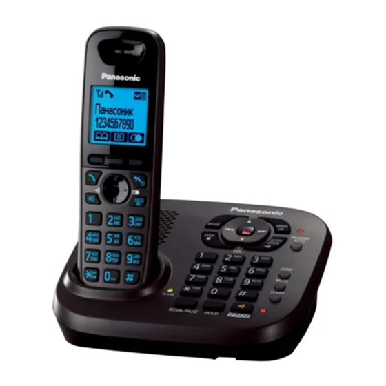
- Page 1 (for Middle Near East and Other Areas) KX-TGA651BXT KX-TG6561BXT (Base Unit) (Handset) Configuration for each model Model No Base Unit Handset Charger Unit KX-TG6561 1 (TG6561) 1 (TGA651) © Panasonic System Networks Co., Ltd. 2010 Unauthorized copying and distribution is a violation of law.
- Page 2 KX-TG6561BXT/KX-TGA651BXT WARNING This service information is designed for experienced repair technicians only and is not designed for use by the general public. It does not contain warnings or cautions to advise non-technical individuals of potential dangers in attempting to service a product. Products powered by electricity should be serviced or repaired only by experienced professional technicians.
-
Page 3: Table Of Contents
KX-TG6561BXT/KX-TGA651BXT TABLE OF CONTENTS PAGE PAGE 1 Safety Precautions----------------------------------------------- 4 15.1. Cabinet and Electrical Parts (Base Unit) ----------- 83 1.1. For Service Technicians --------------------------------- 4 15.2. Cabinet and Electrical Parts (Handset)------------- 84 2 Warning -------------------------------------------------------------- 4 15.3. Accessories------------------------------------------------ 85 2.1. Battery Caution--------------------------------------------- 4 15.4. -
Page 4: Safety Precautions
KX-TG6561BXT/KX-TGA651BXT 1 Safety Precautions 1.1. For Service Technicians • Repair service shall be provided in accordance with repair technology information such as service manual so as to prevent fires, injury or electric shock, which can be caused by improper repair work. -
Page 5: Discarding Of P.c. Board
KX-TG6561BXT/KX-TGA651BXT 2.2.1. Suggested PbF Solder There are several types of PbF solder available commercially. While this product is manufactured using Tin, Silver, and Copper (Sn+Ag+Cu), you can also use Tin and Copper (Sn+Cu) or Tin, Zinc, and Bismuth (Sn+Zn+Bi). Please check the manufacturer’s specific instructions for the melting points of their products and any precautions for using their product with other materials. -
Page 6: Specifications
KX-TG6561BXT/KX-TGA651BXT 3 Specifications Power source (AC Adaptor): Standard: DECT(Digital Enhanced Cordless 100–240 V AC, 50/60 Hz Telecommunications), Base unit: PQLV219BXY Power consumption GAP (Generic Access Profile) Base unit: Number of channels: 120 Duplex Channels Standby: Approx. 0.6 W Maximum: Approx. 4.0 W Frequency range: 1.88 GHz to 1.90 GHz... -
Page 7: Technical Descriptions
KX-TG6561BXT/KX-TGA651BXT 4 Technical Descriptions 4.1. Block Diagram (Base Unit_Main) -
Page 8: Block Diagram (Base Unit_Rf Part)
KX-TG6561BXT/KX-TGA651BXT 4.2. Block Diagram (Base Unit_RF Part) ANT2 ANT2 ANT1 DA801 TXON RXON ANT1 KX-TG6561 BLOCK DIAGRAM (Base Unit_RF Part) -
Page 9: Circuit Operation (Base Unit)
KX-TG6561BXT/KX-TGA651BXT 4.3. Circuit Operation (Base Unit) General Description: (BBIC, Flash Memory, EERROM) is a digital speech/signal processing system that implements all the functions of speech compression, record and playback, and memory management required in a digital telephone answering machine. The BBIC system is fully controlled by a host processor. The host processor provides activation and control of all that functions as follows. - Page 10 KX-TG6561BXT/KX-TGA651BXT 4.3.4. Power Supply Circuit/Reset Circuit The power supply voltage from AC adaptor is converted to VBAT (3.0V) in IC302. And +3.0V for peripherals and analog part is insulated from VBAT by Doubler of BBIC. Circuit Operation: +3.0V VBAT IC601...
- Page 11 KX-TG6561BXT/KX-TGA651BXT 4.3.4.1. Charge Circuit The voltage from the AC adaptor is supplied to the charge circuits. +6.5V F301 CHARGE+ CHARGE-...
- Page 12 KX-TG6561BXT/KX-TGA651BXT 4.3.5. Telephone Line Interface Telephone Line Interface Circuit: Function • Bell signal detection • ON/OFF hook and pulse dial circuit • Side tone circuit Bell signal detection and OFF HOOK circuit: In the idle mode, Q141 is open to cut the DC loop current and decrease the ring load. When ring voltage appears at the Tip (T) and Ring (R) leads (When the telephone rings), the AC ring voltage is transferred as follows: T →...
- Page 13 KX-TG6561BXT/KX-TGA651BXT 4.3.6. Parallel Connection Detect Circuit/Auto Disconnect Circuit Function: In order to disable call waiting and stutter tone functions when using telephones connected in parallel, it is necessary to have a circuit that judges whether a telephone connected in parallel is in use or not. This circuit determines whether the telephone connected in parallel is on hook or off hook by detecting changes in the T/R voltage.
- Page 14 KX-TG6561BXT/KX-TGA651BXT 4.3.7. Transmitter/Receiver • Audio Circuits and DTMF tone signal circuits. Base Unit and Handset mainly consist of RF Module and DECT BBIC. Base Unit and Handset transmit/receive voice signal and data signal through the antenna on carrier frequency. Signal Path: *Refer to Signal Route (P.17).
-
Page 15: Block Diagram (Handset)
KX-TG6561BXT/KX-TGA651BXT 4.4. Block Diagram (Handset) -
Page 16: Circuit Operation (Handset)
KX-TG6561BXT/KX-TGA651BXT 4.5. Circuit Operation (Handset) 4.5.1. Outline Handset consists of the following ICs as shown in Block Diagram (Handset) (P.15). • DECT BBIC (Base Band IC): IC1 - All data signals (forming/analyzing ACK or CMD signal) - All interfaces (ex: Key, Detector Circuit, Charge, DC/DC Converter, EEPROM, LCD, RF Power Amp.) -
Page 17: Signal Route
KX-TG6561BXT/KX-TGA651BXT 4.6. Signal Route ROUTE SIGNAL ROUTE HANDSET TX <HANDSET_RF_TX_ROUTE> - ANT. --- ---ANT. - <BASE_UNIT_RF_RX_ROUTE> - IC501(46/47 - 28) - R181 - C184 - Q161 - Q141 - D101 - L101/[L102 - P101] - T/R(TEL LINE) HANDSET RX T/R(TEL LINE) - L101/[P101 - L102] - D101 - Q141 - R165 - C173 - Q171 - C178 - R178 - IC501(16 - 44/45) - <BASE_UNIT_RF_TX_ROUTE>... - Page 18 KX-TG6561BXT/KX-TGA651BXT SIGNAL ROUTE ROUTE HANDSET RF IC1(44/45) - L809 - C812 - DA801 - C895 - ANT [ TX_ROUTE ] HANDSET RF ANT - C895 - DA801 - C826 - IC1(46/47) [ RX_ROUTE ] IC501(44/45) - C812 - L809 - DA801 - C895 - DA802 - C893/C894 - ANT1/ANT2...
-
Page 19: Location Of Controls And Components
KX-TG6561BXT/KX-TGA651BXT 5 Location of Controls and Components Refer to the Operating Instructions. Note: You can download and refer to the Operating Instructions (Instruction book) on TSN Server. 6 Installation Instructions Refer to the Operating Instructions. Note: You can download and refer to the Operating Instructions (Instruction book) on TSN Server. -
Page 20: Service Mode
KX-TG6561BXT/KX-TGA651BXT 8 Service Mode 8.1. Engineering Mode 8.1.1. Base Unit Important: Make sure the address on LCD is correct when entering new data. Otherwise, you may ruin the unit. Soft keys {ic} (Off/Power) Naviga tor key/ (Volume) key {ECO/R} ECO: Eco mode shortcut key... - Page 21 KX-TG6561BXT/KX-TGA651BXT Frequently Used Items (Base Unit) ex.) Items Address Default Data New Data Remarks Frequency 00 08/00 07 01/00 Use these items in a READ-ONLY mode to confirm the contents. Careless rewriting may 00 02~00 06 Given value cause serious damage to the computer system.
- Page 22 KX-TG6561BXT/KX-TGA651BXT 8.1.2. Handset Important: Make sure the address on LCD is correct when entering new data. Otherwise, you may ruin the unit. Soft keys {ic} (Off/Power) Naviga tor key/ (Volume) key {ECO/R} ECO: Eco mode shortcut key R: Recall/Flash Dial keypad...
- Page 23 KX-TG6561BXT/KX-TGA651BXT Frequently Used Items (Handset) ex.) Items Address Default Data New Data Possible Adjusted Possible Adjusted Remarks Value MAX (hex) Value MIN (hex) Sending level 03 17 Adjusted value Given value (*2) Receiving level 03 18 Adjusted value Given value...
-
Page 24: Copying Phonebook Items When Repairing
KX-TG6561BXT/KX-TGA651BXT 8.2. Copying Phonebook Items when Repairing You can copy the handset phonebook to another (compatible Panasonic) handset. This will help to save the original phonebook data which the customer has registered. Refer to the following procedures. Phonebook data is stored in a handset. - Page 25 KX-TG6561BXT/KX-TGA651BXT Case 3: A handset has a defect. (Radio transmission is functioning.) Service center has a normal HS (B). HS (A) HS (A) HS (B) BS (A) BS (A) 1. Cancel HS (A). 2. Register HS (B) as a handset no. 1.
-
Page 26: How To Clear User Setting
KX-TG6561BXT/KX-TGA651BXT 8.3. How to Clear User Setting Units are reset to the Factory settings by this operation (Erase recorded Voice messages*, stored Phone numbers, Caller list and etc.) Note: • Some menus are not reset. Refer to Operating Instructions (P.19). -
Page 27: Troubleshooting Guide
KX-TG6561BXT/KX-TGA651BXT 9 Troubleshooting Guide 9.1. Troubleshooting Flowchart Flow Chart FLOW CHART Not working Power ON Base Unit Check Power Not playback Playback Pre-Message Check Playback Not record Record Check Record Link No link No charge Battery Charge Check Battery Charge... - Page 28 KX-TG6561BXT/KX-TGA651BXT 9.1.1. Check Power 9.1.1.1. Base Unit Is the AC Adaptor inserted into AC outlet? (*1) Is the AC Adaptor inserted into AC outlet? (*1) AC Adaptor. Is output voltage of AC adaptor 6.5 V? Check Check Power Supply Circuit.
- Page 29 KX-TG6561BXT/KX-TGA651BXT 9.1.2. Check Record 9.1.2.1. Base Unit Not record Incoming Message Check Telephone Line Interface Check Bell signal. [Bell]. Check Telephone Line Interface Does the unit catch line? [OFF HOOK]. Check Line In: Pin 16 of BBIC. Check ICM Recording in Signal Route.
- Page 30 KX-TG6561BXT/KX-TGA651BXT 9.1.3. Check Playback 9.1.3.1. Base Unit Check VDDC (1.2 V): Test Point [VDDC] Check Power Supply Circuit. Check output of BBIC (Pin 29, 31). Check BBIC and Flash Memory. Check Speaker and its surroundings. Cross Reference: Note: Power Supply Circuit/Reset Circuit (P.10) Flash Memory is IC601.
- Page 31 KX-TG6561BXT/KX-TGA651BXT 9.1.5. Check Link 9.1.5.1. Base Unit Does Base Unit make link with normal working Base Unit is OK. Check Handset. Handset? Is the voltage of VBAT about 3.0 V? Check around Power Supply Circuit. Refer to Check Point...(A) Is the voltage of VDDC about 1.2 V? Refer to Check Point...(B)
- Page 32 KX-TG6561BXT/KX-TGA651BXT Is the Frequency Drift OK? Refer to Check Point...(M). Is the Sensitivity Receiver OK? Refer to Check Point...(N). Is the Timing OK? Replace with a new Circuit Board. Refer to Check Point...(O). Is the Power RAMP OK? Refer to Check Point...(P).
- Page 33 KX-TG6561BXT/KX-TGA651BXT 9.1.5.2. Handset Does Handset make link with Base Unit? Handset is OK. Check Base Unit. (Correct working unit) Is the voltage of "1.8V" about 1.8 V? Adjust C10 voltage to 1.8 V. Refer to Check Point...(A). Refer to Check Point...(A).
- Page 34 KX-TG6561BXT/KX-TGA651BXT Is the Frequency Drift OK? Refer to Check Point...(N). Is the Sensitivity Receiver OK? Refer to Check Point...(O). Is the Power RAMP OK? Replace with a new Circuit Board. Refer to Check Point...(P). Cross Reference: Check Point (Handset) (P.44)
- Page 35 KX-TG6561BXT/KX-TGA651BXT 9.1.6. Check the RF part 9.1.6.1. Finding out the Defective part 1. Prepare Regular HS(*1) and Regular BU(*2). 2. a. Re-register regular HS (Normal mode) to base unit (to be checked). If this operation fails in some ways, the base unit is defective.
- Page 36 KX-TG6561BXT/KX-TGA651BXT 9.1.6.2. RF Check Flowchart Each item (1 ~ 3) of RF Check Flowchart corresponds to Check Table for RF part (P.37). Please refer to the each item. Start Link Control Check DSP interface parts. confirmation signal (RF Block <->DSP on BU/HS P.C.B)
- Page 37 KX-TG6561BXT/KX-TGA651BXT 9.1.6.3. Check Table for RF part Item BU (Base Unit) Check HS (Handset) Check Link Confirmation Normal 1. Register Regular HS to BU (to be 1. Register HS (to be checked) to Regular checked). HS, BU Mode: [Normal mode] 2.
- Page 38 KX-TG6561BXT/KX-TGA651BXT 9.1.7. Registering a Handset to the Base Unit The supplied handset and base unit are pre-registered. If for some reason the handset is not registered to the base unit (for example, _ is displayed even when the handset is near the base unit), re-register the handset.
- Page 39 KX-TG6561BXT/KX-TGA651BXT 9.1.9. Check Handset Transmission Check MIC of Handset. Check CDL TX (HANDSET) in Signal Route. Cross Reference: Signal Route (P.17) 9.1.10. Check Handset Reception Check Handset Speaker in How to check the Handset Speaker or Receiver. Check CDL RX (HANDSET) in Signal Route.
- Page 40 KX-TG6561BXT/KX-TGA651BXT 9.1.12. Bell Reception 9.1.12.1. Base Unit Check around R111, R112, R113, R114, Q111, When bell signal is coming, is there bell sound D113, C111, C112, signal at BBIC (IC501: 59)? When bell signal is coming, is there bell sound Check around L474, L475.
-
Page 41: Troubleshooting By Symptom (Base Unit And Charger Unit)
KX-TG6561BXT/KX-TGA651BXT 9.2. Troubleshooting by Symptom (Base Unit and Charger Unit) If your unit has below symptoms, follow the instructions in remedy column. Remedies depend on whether you have DECT tester (*1) or not. Remedy (*2) Symptom You have DECT Tester. - Page 42 KX-TG6561BXT/KX-TGA651BXT Items Check Procedure Check or Point Replace Parts 1. Connect Telephone Socket to DTMF tester. (Load=600 Ω) (I) DTMF Generator Check R181, C184, 2. Link Handset and push dial key. Q161, D141 3. Confirm DTMF character. 4. Confirm that the high Group is -6.0 ± 2dBm.
- Page 43 KX-TG6561BXT/KX-TGA651BXT Items Check Procedure Check or Point Replace Parts (O)* Timing Confirmation Follow steps 1 to 6 of (J). IC501, C805, ANT 1 7.Confirm that the Timing accuracy is C806, C810, • ± 5.0 ppm (When adjust the frequency of CLK in item (G)).
-
Page 44: Troubleshooting By Symptom (Handset)
KX-TG6561BXT/KX-TGA651BXT 9.3. Troubleshooting by Symptom (Handset) If your unit has below symptoms, follow the instructions in remedy column. Remedies depend on whether you have DECT tester (*1) or not. Remedy (*2) Symptom You have DECT Tester. You don't have DECT Tester. - Page 45 KX-TG6561BXT/KX-TGA651BXT Items Check Procedure Check or Point Replace Parts (F)* Battery Monitor Check 1. Apply 2.25 V between BATT+ and BATT-. IC1, F1, C1, 2. Execute the command sendchar PAD sendchar LED 0 sendchar CRX 0 1 sendchar AD1 It assumes that the return value is XX.
- Page 46 KX-TG6561BXT/KX-TGA651BXT Items Check Procedure Check or Point Replace Parts (K)* Frequency Offset Follow steps 1 to 3 of (I). IC1, Confirmation 4.Confirm that the frequency Offset is < ± 50 kHz. C802~C806, C808~C814, C819~C820, C822, C825~C827, C834, C860~C864, L801~L804, DA801,...
- Page 47 KX-TG6561BXT/KX-TGA651BXT 9.3.2. Troubleshooting for Speakerphone When the customer’s telephone line corresponds to the following conditions, and the transmission signal of SP-Phone is interrupted, performing the next set up to a cordless handset will improve it to some extent. Conditions 1. When customer’s line has less line loss.
-
Page 48: Disassembly And Assembly Instructions
KX-TG6561BXT/KX-TGA651BXT 10 Disassembly and Assembly Instructions 10.1. Disassembly Instructions 10.1.1. Base Unit Remove the 5 screws to remove the cabinet cover. Remove the tapes and solders. Cabinet cover Remove the screw . Remove the parallel wires to remove Main P.C. board the main P.C. - Page 49 KX-TG6561BXT/KX-TGA651BXT Remove the 2 screws to remove 2 screws the jack holder. Remove the 4 screws to remove the operational P.C. board. 4 screws Jack holder Operational P.C. board...
- Page 50 KX-TG6561BXT/KX-TGA651BXT 10.1.2. Handset 2 screws Remove the 2 screws. Insert a JIG (PQDJ10006Y) between the cabinet body Cabinet body and the cabinet cover, then pull it along the gap to open the cabinet. Cabinet cover Likewise, open the other side of the cabinet.
-
Page 51: How To Replace The Handset Lcd
KX-TG6561BXT/KX-TGA651BXT 10.2. How to Replace the Handset LCD Note: The illustrations are simplified in this page. They may differ from the actual product. P. C. board Vertical Interval Tolerance Peel off the FFC (Flexible Flat Cable) from 0.2 mm the LCD, in the direction of the arrow. Take care to ensure that the foil on the P.C. -
Page 52: Measurements And Adjustments
KX-TG6561BXT/KX-TGA651BXT 11 Measurements and Adjustments This chapter explains the measuring equipment, the JIG connection, and the PC setting method necessary for the measurement in Troubleshooting Guide (P.27) 11.1. Equipment Required • Digital multi-meter (DMM): it must be able to measure voltage and current. - Page 53 KX-TG6561BXT/KX-TGA651BXT 11.2.2. How to install Batch file into P.C. Insert the Batch file CD-ROM into CD-ROM drive and copy PNZZTG**** folder to your PC (example: D drive). <Example for Windows> On your computer, click [Start], select Programs Open an MS-DOS mode window.
-
Page 54: Adjustment Standard (Base Unit)
KX-TG6561BXT/KX-TGA651BXT 11.3. Adjustment Standard (Base Unit) When connecting the simulator equipment for checking, please refer to below. 11.3.1. Bottom View C301 F301 3.0A +6.5V R116 C311 R301 R118 R302 C303 C310 C116 C104 D104 R122 IC301 R103 Q111 C103 C309... -
Page 55: The Setting Method Of Jig (Handset)
KX-TG6561BXT/KX-TGA651BXT 11.4. The Setting Method of JIG (Handset) This section explains the PC setting to use command required in Check Point (Handset)(P.44). <Preparation> (PQZZ1CD505E), change following values • Serial JIG cable: PQZZ1CD300E* resistance. Then you can use it as a JIG Cable for both •... - Page 56 KX-TG6561BXT/KX-TGA651BXT 11.4.2. How to install Batch file into P.C. Insert the Batch file CD-ROM into CD-ROM drive and copy PNZZTG***** folder to your PC (example: D drive). <Example for Windows> Open an MS-DOS mode window. On your computer, click [Start], select Programs...
-
Page 57: Adjustment Standard (Handset)
KX-TG6561BXT/KX-TGA651BXT 11.5. Adjustment Standard (Handset) When connecting the simulator equipments for checking, please refer to below. 11.5.1. Component View KX-TGA650XX KX-TGA651XX PNLB1734Y KX-TGA250XX KX-TGA251XX KX-TGA403XX TP_ANT1 TGA650XX TGA651XX C152 C175 R578 TGA250XX TGA251XX TGA403XX C106 C200 C201 R231 C104 C107... -
Page 58: Things To Do After Replacing Ic Or X'tal
KX-TG6561BXT/KX-TGA651BXT 11.6. Things to Do after Replacing IC or X'tal If repairing or replacing BBIC (FLASH type), EEPROM and X'tal, it is necessary to download the required data such as Programming data or adjustment data, etc in memory. The set doesn't operate if it is not executed. - Page 59 KX-TG6561BXT/KX-TGA651BXT 11.6.1.2. Handset First, operate the PC setting according to The Setting Method of JIG (Handset)(P.55). Then download the appropriate data according to the following procedures. Items How to download/Required adjustment BBIC (FLASH type) Programming data is stored in memory.
-
Page 60: Rf Specification
KX-TG6561BXT/KX-TGA651BXT 11.7. RF Specification 11.7.1. Base Unit Item Value Refer to -. * TX Power 19 dBm ~ 25 dBm Check Point (Base Unit) (J) Modulation -370±30/+370±30 kHz/div & Modulated Check Point (Base Unit) (K) width 690 kHz Frequency Offset... -
Page 61: How To Check The Handset Speaker Or Receiver
KX-TG6561BXT/KX-TGA651BXT 11.8. How to Check the Handset Speaker or Receiver 1. Prepare the digital voltmeter, and set the selector knob to ohm meter. 2. Put the probes at the speaker terminals as shown below. SPEAKER: Is the value between (+) terminal and (–) terminal about 8 Ω? -
Page 62: Miscellaneous
KX-TG6561BXT/KX-TGA651BXT 12 Miscellaneous 12.1. How to Replace the Flat Package IC Even if you do not have the special tools (for example, a spot heater) to remove the Flat IC, with some solder (large amount), a soldering iron and a cutter knife, you can easily remove the ICs that have more than 100 pins. - Page 63 KX-TG6561BXT/KX-TGA651BXT 12.1.3. How to Install the IC 1. Temporarily fix the FLAT PACKAGE IC, soldering the two marked pins. *Check the accuracy of the IC setting with the corresponding soldering foil. 2. Apply flux to all pins of the FLAT PACKAGE IC.
-
Page 64: How To Replace The Llp
KX-TG6561BXT/KX-TGA651BXT 12.2. How to Replace the LLP (Leadless Leadframe Package) IC Note: This description is only applied on the model with Shield case. 12.2.1. Preparation • PbF (: Pb free) Solder • Soldering Iron Tip Temperature of 700 °F ± 20 °F (370 °C ± 10 °C) Note: We recommend a 30 to 40 Watt soldering iron. - Page 65 KX-TG6561BXT/KX-TGA651BXT 12.2.4. How to Install the IC 1. Place the solder a little on the land where the radiation GND pad on IC bottom is to be attached. Soldering Iron Land Solder P.C.Board 2. Place the solder a little on the land where IC pins are to be attached, then place the IC.
-
Page 66: How To Replace The Shield Case
KX-TG6561BXT/KX-TGA651BXT 12.3. How to Replace the Shield Case 12.3.1. Preparation • PbF (: Pb free) Solder • Soldering Iron Tip Temperature of 700°F ± 20°F (370°C ± 10°C) Note: We recommend a 30 to 40 Watt soldering iron. An expert may be able to use a 60 to 80 Watt iron where someone with less experience could overheat and damage the PCB foil. - Page 67 KX-TG6561BXT/KX-TGA651BXT 12.3.4. How to Install the Shield Case Note: • If you don’t have special tools (ex. Hot air disordering tool), conduct the following operations. • Shield case’s No. : PNMC1013Z 1. Put the shield case. 2. Solder the surroundings.
-
Page 68: Terminal Guide Of The Ics, Transistors, Diodes And Electrolytic Capacitors
KX-TG6561BXT/KX-TGA651BXT 12.4. Terminal Guide of the ICs, Transistors, Diodes and Electrolytic Capacitors 12.4.1. Base Unit (Reverse View) 2SC6054JSL, PQVTBF822T7 PNWI2G6561EH UNR92A6J0L, UNR92A9J0L PNWITG6521EH 2SB1218A, UNR92A2J0L B1ZBZ0000065 B1GFCFEN0011 B1ABCE000009 C0DBAGZ00026 C2HBCY000059 Cathode Cathode Anode MA111 Anode PQVDRLZ20A B0BC3R4A0006 B1ACGP000007 2SD0874AS B0EDER000009... -
Page 69: Schematic Diagram
KX-TG6561BXT/KX-TGA651BXT 13 Schematic Diagram 13.1. For Schematic Diagram 13.1.1. Base Unit (Schematic Diagram (Base Unit)) Notes: 1. DC voltage measurements are taken with voltmeter from the negative voltage line. 2. The schematic diagrams may be modified at any time with the development of new technology. -
Page 70: Schematic Diagram (Base Unit)
KX-TG6561BXT/KX-TGA651BXT 13.2. Schematic Diagram (Base Unit) ANT2 R807 C892 RXON ANT1 C822 C827 W 0.2mm W 0.15mm R498 L 20mm 1st layer 3rd layer C894 C826 R499 W 0.2mm C820 L 10mm 1.5p 1st layer ANT2 DA801 C805 C895 C812 L809 2.7p... - Page 71 KX-TG6561BXT/KX-TGA651BXT VCCA *R160 Q143 Q141 +3.0V *Q161 R141 C101 680p C165 C163 100k D101 C173 *R164 R161 *R149 *Q140 R172 100k 0.22u 2.7k 100k Q142 C102 680p R151 *R145 C175 100k 2.2k 1000p P101 MIP MIN *Q171 C174 L474 *C178...
-
Page 72: Schematic Diagram (Base Unit_Operation)
KX-TG6561BXT/KX-TGA651BXT 13.3. Schematic Diagram (Base Unit_Operation) KEY5 KEY4 KEY3 KEY2 KEY1 KEY0 NEWMSG2 STOP NEWMSG ERASE ROW4 CN1-5 CN1-6 CN1-7 AUTO SP-PHONE MUTE CN1-8 ROW3 CN1-9 CN1-10 CN2-2 CN2-3 CN2-4 GREETING REDIAL CN2-5 ROW2 CN2-6 SKIP DOWN IN USE_LED LED1... - Page 73 KX-TG6561BXT/KX-TGA651BXT Memo...
-
Page 74: Schematic Diagram (Handset)
KX-TG6561BXT/KX-TGA651BXT 13.4. Schematic Diagram (Handset) Charge Current BATTERY BATT+ 5.6n C340 C341 C342 C1CP1 R406 J39p +1.8V 6.3V R407 BATTERY 330u (MAX500mA) +1.8V BATTERY R401 1.8V 1.8V BATT- D400 R330 R400 Q400 C400 C331 J56p 6.3V K2.2u R331 C332 330u... - Page 75 KX-TG6561BXT/KX-TGA651BXT R807 W 0.15mm RXON L 20+/-2mm 3rd layer C827 L801 TP_ANT1 *C826 RX_RF C803 RF_RXn 1.5p DA801 BATTERY RF_RXp W 0.125mm L 7.6mm Gap 0.125mm W 0.15mm W 0.15mm CP+3.0V 1st layer L 5.0mm L 5.0mm 1st layer 1st layer...
- Page 76 KX-TG6561BXT/KX-TGA651BXT Memo...
-
Page 77: Printed Circuit Board
KX-TG6561BXT/KX-TGA651BXT 14 Printed Circuit Board 14.1. Circuit Board (Base Unit_Main) 14.1.1. Component View PNLB1152Z ANT1 P101 ANT2 R112 R371 C306 R332 C331 D101 DA802 C341 C895 C892 C822 R123 C825 C814 DA801 C891 C827 R141 C898 C826 C517 C899 C863... - Page 78 KX-TG6561BXT/KX-TGA651BXT 14.1.2. Bottom View C301 F301 3.0A +6.5V R116 C311 R301 R118 R302 C303 C310 C116 C104 D104 R122 IC301 R103 Q111 C103 C309 DCDC_OUT VBAT Q302 D301 STM/CKM/P15 (13.824 MHz) R306 GND2 VDDC D133 (1.2V) C601 C530 C120 D132...
-
Page 79: Circuit Board (Base Unit_Operation)
KX-TG6561BXT/KX-TGA651BXT 14.2. Circuit Board (Base Unit_Operation) 14.2.1. Component View KX-TG7341H TG7331H LED4 LED3 ERASE SKIP DOWN PNLB1038Z PROGRAM MUTE LED1 RECALL LED2 SP-PHONE KX-TG6561 CIRCUIT BOARD (Base Unit_Operation (Component View)) - Page 80 KX-TG6561BXT/KX-TGA651BXT 14.2.2. Bottom View KX-TG7341H TG7331H PNLB1038Z PNWH01 PNWH02 KX-TG6561 CIRCUIT BOARD (Base Unit_Operation (Bottom View))
-
Page 81: Circuit Board (Handset)
KX-TG6561BXT/KX-TGA651BXT 14.3. Circuit Board (Handset) 14.3.1. Component View KX-TGA650XX KX-TGA651XX PNLB1734Y KX-TGA250XX KX-TGA251XX KX-TGA403XX TP_ANT1 RCV+ RCV- TGA650XX TGA651XX C152 C175 R578 TGA250XX TGA251XX TGA403XX C106 C200 R231 C201 C104 C107 C105 C103 C206 C203 R236 C863 C864 C814 C811... - Page 82 KX-TG6561BXT/KX-TGA651BXT 14.3.2. Bottom View LED12 PNLB1734Y KX-TGA650XX KX-TGA651XX KX-TGA250XX KX-TGA251XX KX-TGA403XX TGA650XX TGA651XX CN51 TGA250XX TGA251XX TGA403XX SOFT_A SOFT_B SOFT_C TALK LEFT RIGHT LED8 LED6 DOWN KX-TGA651 CIRCUIT BOARD (Handset_Main (Bottom View))
-
Page 83: Cabinet And Electrical Parts (Base Unit)
KX-TG6561BXT/KX-TGA651BXT 15 Exploded View and Replacement Parts List 15.1. Cabinet and Electrical Parts (Base Unit) PCB2 15 (*1) PCB1 MIC1 Ref.No. Figure 2.6 x 8 mm Note: (*1) The SPACERs (No.15) are cut from the excess parts of SPACER (No.107) of Cabinet and Electrical Parts (Handset) -
Page 84: Cabinet And Electrical Parts (Handset)
(*1) This cable is fixed by welding. Refer to How to Replace the Handset LCD (P.51). (*2) The rechargeable Ni-MH battery HHR-4DPA or HHR-4MRT is available through sales route of Panasonic. (*3) Attach the spacer (No. 119) to the exact location described above. -
Page 85: Accessories
KX-TG6561BXT/KX-TGA651BXT 15.3. Accessories... -
Page 86: Replacement Part List
KX-TG6561BXT/KX-TGA651BXT 15.4. Replacement Part List Safety Ref. Part No. Part Name & Description Remarks 1. RTL (Retention Time Limited) K2ECYZ000001 JACK, DC Note: PNLA1030Z ANTENNA The “RTL” marking indicates that its Retention Time is PNYE1029Z SPACER, ANTENNA PQMG10025W RUBBER PARTS, MIC Limited. - Page 87 KX-TG6561BXT/KX-TGA651BXT Safety Ref. Part No. Part Name & Description Remarks Safety Ref. Part No. Part Name & Description Remarks R112 PQ4R10XJ333 C111 F1J2A473A024 0.047 R113 ERJ3GEYJ183 C112 F1J2A473A024 0.047 R114 ERJ2GEJ683 C113 PQCUV1H103KB 0.01 R115 ERJ3GEYJ565 5.6M C114 F1J2A473A024 0.047...
- Page 88 KX-TG6561BXT/KX-TGA651BXT 15.4.2.2. Main P.C.Board Parts Safety Ref. Part No. Part Name & Description Remarks Note: C811 F1G1H1R0A480 1p (*1) Reconfirm the model No. written on the handset’s name C812 F1G1H100A723 10p plate when replacing PCB100. Because the model No. of...
- Page 89 KX-TG6561BXT/KX-TGA651BXT Safety Ref. Part No. Part Name & Description Remarks Safety Ref. Part No. Part Name & Description Remarks ERJ2GEJ100 C332 ECUE0J105KBQ 1 ERJ2GEJ102 C341 ECUE1H390JCQ 39p ERJ2GEJ821 C580 F1G1H100A723 10p ERJ2GEJ821 C802 F1G1H2R0A480 2.0p ERJ3GEYJ152 1.5k C803 F1G1H1R5A480 1.5p...
- Page 90 KX-TG6561BXT/KX-TGA651BXT KXTG6561BXT KXTGA651BXT...
Need help?
Do you have a question about the KX-TG6561BXT and is the answer not in the manual?
Questions and answers