Table of Contents
Advertisement
Quick Links
General Description
This document describes the SLA7070MPRT series,
which are unipolar 2-phase stepping motor driver ICs. The
SLA7070MPRT series employs a clock input method as
a control signal input method, enabling full control of the
device operation using only a few signal lines, instead of
the conventional phase input method that requires about 10
signal lines. This allows simplification of the circuit design
and a reduced workload on the control microprocessor.
In addition, the SLA7070MPRT series is improved in its
reliability by preventing the IC from damage due to abnor-
mal conditions. For example, it has a flag output terminal
to signal that a protection circuit has operated. The series
also has a built-in protection circuitry against motor coil
opens/shorts and thermal shutdown protection as well.
All the SLA7070MPRT series ICs are compatible in their
pin layouts and interface specifications, allowing custom-
ers the flexibility of choosing the IC that is optimal for the
target equipment characteristics.
Features and Benefits
• Power supply voltages, V
BB
normal operating range
• Logic supply voltages, V
DD
• Maximum output currents: 1 A, 1.5 A, 2 A, 3 A
• Built-in sequencer
• Full-, half-, and microstepping available (microstepping
options are capable of full-, half-, quarter-, eighth-, and
sixteenth-stepping
The SLA7070MPRT series product variants and optional features
Part Number
SLA7070MPRT
SLA7071MPRT
SLA7072MPRT
SLA7073MPRT
SLA7075MPRT
SLA7076MPRT
SLA7077MPRT
SLA7078MPRT
SLA7070MPRT-AN, Rev. 2.1
January 10, 2013
SLA7070MPRT Series Unipolar 2-Phase
: 46 V (max.), 10 to 44 V
: 3.0 to 5.5 V
Output Current
Stepping
Rate
Full and
half step
Microstep
SANKEN ELECTRIC CO., LTD.
http://www.sanken-ele.co.jp/en/
Application Information
Stepper Motor Driver ICs
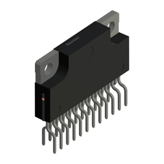
Figure 1. SLA7070MPRT packages are fully molded ZIPs with an
exposed pad for heatsink mounting.
• Built-in sense resistor, R
• All variants are pin-compatible for enhanced
design flexibility
• ZIP type 23-pin molded package (SLA package)
• Self-excitation PWM current control with fixed off-time
(microstepping options off-time adjusted automatically by
step reference current ratio; 3 levels)
• Built-in synchronous rectifying circuit reduces losses at
PWM-off
• Synchronous PWM chopping function prevents motor
noise in Hold mode
• Sleep mode for reducing the IC input current in
stand-by state
• Built-in protection circuitry against motor coil
opens/shorts and thermal shutdown protection options
Applications
• LBPs, PPCs, ATMs, industrial robots, and so forth
Input Clock
Edge Detection
(I
)
OUT
(A)
Standard
1
1.5
Rising (positive)
edge
2
3
1
1.5
Rising (positive)
edge
2
3
SInt
Blanking Time
(µs)
Standard
3.2
1.7
Advertisement
Table of Contents

Related Manuals for Sanken SLA7070MPRT Series

Summary of Contents for Sanken SLA7070MPRT Series
- Page 1 In addition, the SLA7070MPRT series is improved in its reliability by preventing the IC from damage due to abnor- mal conditions. For example, it has a flag output terminal •...
-
Page 2: Table Of Contents
) and Main Power Supply Voltage (V Internal Logic Circuits Reset Clock Input Chopping Synchronous Circuit Output Disable (Sleep1 and Sleep2) Circuits 31 Ref/Sleep1 Pin Logic Input Pins Thermal Design Information Characteristic Data SLA7070MPRT-AN, Rev. 2.1 SANKEN ELECTRIC CO., LTD. -
Page 3: Specifications
Output from protection circuits monitor SenseB Phase B current sensing ¯ O ¯ ¯ u ¯ ¯ t ¯ ¯ B ¯ Output of phase B ¯ 20, 21 22, 23 OutB Output of phase B SLA7070MPRT-AN, Rev. 2.1 SANKEN ELECTRIC CO., LTD. - Page 4 Output from protection circuits monitor SenseB Phase B current sensing ¯ O ¯ ¯ u ¯ ¯ t ¯ ¯ B ¯ Output of phase A ¯ 20, 21 22, 23 OutB Output of phase B SLA7070MPRT-AN, Rev. 2.1 SANKEN ELECTRIC CO., LTD.
-
Page 5: Package Outline Drawing
3rd and 4th are date of manufacture (01 to 31) Pin Plating: Solder plating (Pb free) Leadframe plating Pb-free. Device composition includes high-temperature solder (Pb >85%), which is exempted from the RoHS directive. SLA7070MPRT-AN, Rev. 2.1 SANKEN ELECTRIC CO., LTD. -
Page 6: Electrical Characteristics
Main Power Supply Voltage – Surge voltage at VDD pin should Logic Supply Voltage be less than ±0.5 V to avoid – malfunctioning in operation Measured at pin 12, without Case Temperature – – °C heatsink SLA7070MPRT-AN, Rev. 2.1 SANKEN ELECTRIC CO., LTD. - Page 7 Flag Output Current –1.25 – – FlagH In a state of: Sleep1, I , output off, and Sequencer enabled. In a condition of V ≥ V , the protection circuit will activate. SENSE SLA7070MPRT-AN, Rev. 2.1 SANKEN ELECTRIC CO., LTD.
- Page 8 Mode 8, 9, A, B, C, D, E, and F – – µs off1 PWM Off-Time Mode 4, 5, 6, and 7 – – µs off2 Mode 1, 2, and 3 – – µs off3 SLA7070MPRT-AN, Rev. 2.1 SANKEN ELECTRIC CO., LTD.
- Page 9 Ω DS(on) Body Diode Forward Voltage = 3 A – 0.95 Sense Resistor* ±3% tolerance 0.150 0.155 0.160 Ω REF Input Voltage Within specified current limit, I = 3.0 A 0.04 – 0.45 *Includes the inherent bulk resistance (approximately 5 mΩ) of the resistor itself. SLA7070MPRT-AN, Rev. 2.1 SANKEN ELECTRIC CO., LTD.
-
Page 10: Allowable Power Dissipation
"prohibition zone" threshold. If the change- over time is too slow, OCP operation will start when V > V SInt Rθj-a= 26. 6℃/W Ambient Temperature, T [℃] Figure 2. Allowable Power Dissipation SLA7070MPRT-AN, Rev. 2.1 SANKEN ELECTRIC CO., LTD. -
Page 11: Typical Application
SYNC) must be pulled up or down to VDD or ground. If 10 kΩ 0.1 μF those unused pins are left open, the device malfunctions. • Unused logic output pins (Mo, Flag) must be kept open. SLA7070MPRT-AN, Rev. 2.1 SANKEN ELECTRIC CO., LTD. -
Page 12: Device Logic
Truth Tables Monitor Output Pin The SLA7070MPRT series provides two device status monitor Common Input Pins Table 1 shows the truth table for input pins common to both outputs: half/full step and microstep variants of the SLA7070MPRT • Flag pin – Protection feature operation series. -
Page 13: Logic Input Pins
5 µs(min) 4 µs(min) 2 µs(min) Clock 2 µs(min) 2 µs(min) 1 µs(min) 1 µs(min) CW/CCW 2 µs(min) 1 µs(min) 1 µs(min) M1, M2, M3 Figure 4. Input Signal Timing. When awakening from Sleep1 or Sleep2 mode, a delay of 100 μs or longer before sending a Clock pulse is recommended. SLA7070MPRT-AN, Rev. 2.1 SANKEN ELECTRIC CO., LTD. -
Page 14: Stepping Sequence Diagrams
Figure 5. Full step; for microstep and full/half step products Sequence Selection Pin Logic Mode Full Step Shows the state to which the stepping sequence progresses at the rising (positive) edge of the Clock input. SLA7070MPRT-AN, Rev. 2.1 SANKEN ELECTRIC CO., LTD. - Page 15 Figure 6. Full step; for microstep and full/half step products Sequence Selection Pin Logic Mode Full Step High Shows the state to which the stepping sequence progresses at the rising (positive) edge of the Clock input. SLA7070MPRT-AN, Rev. 2.1 SANKEN ELECTRIC CO., LTD.
- Page 16 Figure 7. Half step; for microstep and full/half step products Sequence Selection Pin Logic Mode Half Step High 8, F Shows the state to which the stepping sequence progresses at the rising (positive) edge of the Clock input. SLA7070MPRT-AN, Rev. 2.1 SANKEN ELECTRIC CO., LTD.
- Page 17 Figure 8. Half step; for microstep and full/half step products Sequence Selection Pin Logic Mode Half Step High High Shows the state to which the stepping sequence progresses at the rising (positive) edge of the Clock input. SLA7070MPRT-AN, Rev. 2.1 SANKEN ELECTRIC CO., LTD.
- Page 18 RESET … CLOCK 8 38.2 70.7 92.4 Figure 9. Quarter step; for microstep products Sequence Selection Pin Logic Mode Quarter High Step SLA7070MPRT-AN, Rev. 2.1 SANKEN ELECTRIC CO., LTD.
- Page 19 Figure 10. Eighth step; for microstep products Sequence Selection Pin Logic Mode Eighth High High Step Shows the state to which the stepping sequence progresses at the rising (positive) edge of the Clock input. SLA7070MPRT-AN, Rev. 2.1 SANKEN ELECTRIC CO., LTD.
- Page 20 Figure 11. Sixteenth step; for microstep products Sequence Selection Pin Logic Mode Sixteenth High High Step Shows the state to which the stepping sequence progresses at the rising (positive) edge of the Clock input. SLA7070MPRT-AN, Rev. 2.1 SANKEN ELECTRIC CO., LTD.
-
Page 21: Motor Excitation Sequencing
B ¯ B ¯ B ¯ B ¯ B ¯ B ¯ B ¯ B ¯ B ¯ B ¯ B ¯ B ¯ B ¯ B ¯ B ¯ – – Clockwise ∗ Sequence state is Mode 8, but step reference current ratio is Mode F. Mode F has step reference current ratio of 100%, and PWM off-time of 12 μs. SLA7070MPRT-AN, Rev. 2.1 SANKEN ELECTRIC CO., LTD. -
Page 22: Individual Circuit Descriptions
The integrated regulator circuit is used in Regulator Circuit driving the output MOSFET gates and powering other internal Each resistance shown above includes the inherent resistance linear circuits. (approximately 5 mΩ) in the resistor itself. SLA7070MPRT-AN, Rev. 2.1 SANKEN ELECTRIC CO., LTD. -
Page 23: Functional Description
PWM turns on. 5 µs/div 500 ns/div TRIP TRIP Figure 12. Operating waveforms on the Sensex pins during PWM chopping (circled area of left panel is shown in expanded scale in right panel) SLA7070MPRT-AN, Rev. 2.1 SANKEN ELECTRIC CO., LTD. - Page 24 Maximize ringing noise suppression → Large Minimum coil current Small ← Coil current waveform distortion at a → Large high rotation (mainly microstep) Figure 14. Example of a Sensex terminal waveform during hunching phenomenon SLA7070MPRT-AN, Rev. 2.1 SANKEN ELECTRIC CO., LTD.
- Page 25 3.2 μs case has degenerated from an ideal sine wave. Blanking Time: 1.5 µs (typ) typ( Clock SenseA SenseB 500 µs /div Figure 15. Comparison of a Sense terminal waveform during high speed revolution SLA7070MPRT-AN, Rev. 2.1 SANKEN ELECTRIC CO., LTD.
-
Page 26: Pwm Off-Time
Figure 16 shows the difference in back EMF generation between the SLA7060M series and SLA7070MPRT series. The The PWM off-time for the SLA7070MPRT series is controlled SLA7060M series performs on–off operations using only the at a fixed time by an internal oscillator. It also is switched in... -
Page 27: Protection Functions
0.7 V. The output is disabled at the time the protection circuit starts, where V exceeds V . (See figure 17.) In the SLA7070MPRT series, in order to avoid detection mal- functions, when a state of motor disconnection is detected 3 times • (Patent acquired) Driver destruc- Motor Coil Open Protection continuously, the protection functions are enabled (figure 19). - Page 28 Figure 18. Motor coil short circuit protection circuit operation. Overcurrent that flows without passing the sense resistor is undetectable. To recover the circuit after protection operates, VDD must be cycled and started up again. SLA7070MPRT-AN, Rev. 2.1 SANKEN ELECTRIC CO., LTD.
-
Page 29: Application Information
The setting calculation of motor current, I , for the is the target current level, SLA7070MPRT series is determined by the ratios of the external is the motor winding resistance, components R1, R2, and current sense resistor, RS. The following... -
Page 30: On-Off Sequence Of Power Supply (Vbb And Vdd)
Figure 22. Waveform at avalanche breakdown SLA7073M and SLA7078M SLA7072M and SLA7077M SLA7071M and SLA7076M SLA7070M and SLA7075M Product Temperature, T c [°C] Figure 23. SLA7070MPRT iterated avalanche energy tolerated level, E (max) SLA7070MPRT-AN, Rev. 2.1 SANKEN ELECTRIC CO., LTD. -
Page 31: Motor Supply Voltage
Sync signal can be determined by the Clock input signal. When a logic high signal is received on the Clock pin, Because the SLA7070MPRT series has a structure that sepa- rates the control IC (MIC) and the power MOSFETs as shown... -
Page 32: Ref/Sleep1 Pin
(see figure 27). Therefore, let these pins float if they are not used. Thermal Design Information It is not practical to calculate the power dissipation of the SLA7070MPRT series accurately, because that would require ∆T = 26.6 x P factors that are variable during operation, such as time periods and excitation modes during motor rotation, input frequencies = 21.3 x P... - Page 33 CAUTION thermal resistance, R , is a variable used in calculating ΔT θJA The SLA7070MPRT series is designed as a multichip, with The value of R is calculated from the following formula: θFIN separate power elements (MOSFET), control IC (MIC), and ≈R...
-
Page 34: Characteristic Data
Product Temperature, T (°C) Product Temperature, T (°C) SLA7073MPRT/SLA7078MPRT SLA7072MPRT/SLA7077MPRT Io=3A Io=2A Io=2A Io=1A Io=1A 75 100 125 75 100 125 Product Temperature, T (°C) Product Temperature, T Product Temperature, T (°C) (°C) SLA7070MPRT-AN, Rev. 2.1 SANKEN ELECTRIC CO., LTD. - Page 35 75 100 125 Product Temperature, T (°C) Product Temperature, T (°C) SLA7073MPRT/SLA7078MP RT SLA7072MPRT/SLA7077MP RT Io=3A Io=2A Io=2A Io=1A Io=1A 75 100 125 100 125 Product Temperature, T (°C) Product Temperature, T (°C) SLA7070MPRT-AN, Rev. 2.1 SANKEN ELECTRIC CO., LTD.
- Page 36 (aerospace equipment, nuclear power control systems, life support systems, etc.) is strictly prohibited. • In the case that you use Sanken products or design your products by using Sanken products, the reliability largely depends on the degree of derating to be made to the rated values. Derating may be interpreted as a case that an operation range is set by derating the load from each rated value or surge voltage or noise is considered for derating in order to assure or improve the reliability.
Need help?
Do you have a question about the SLA7070MPRT Series and is the answer not in the manual?
Questions and answers