Table of Contents
Advertisement
Quick Links
Advertisement
Table of Contents

Related Manuals for ELTEC BAB 740

Summary of Contents for ELTEC BAB 740
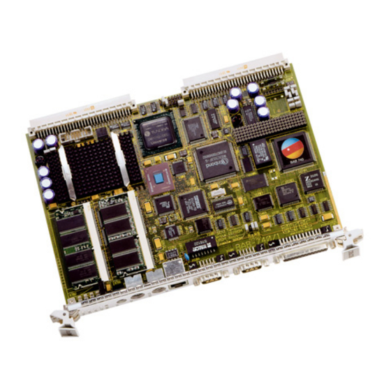
- Page 1 BAB 740 Basic Automation Board with PowerPC 740 manual Revision 2C...
- Page 2 Revision Revision Changes Date / Name First Edition, Valid for Hardware revision 1A 03.01.2000 AR Valid for Hardware revision 3A 24.04.2001 G.M. Valid for Hardware revision 3A 26.09.2001 rae Valid for Software revision W-O9B7-106C - I/O-Address-Map changed - Disclaimer new 08.11.06 hh...
- Page 3 The complete risk inherent in the utilization of this document or in the results of its utilization shall be with the user; to this end, ELTEC Elektronik AG shall not accept any liability. Regardless of the applicability of respective...
- Page 4 manufacturer’s instructions, may cause harmful interference to radio communications. However, there is no guarantee that interference will not occur in a particular installation. If this equipment does cause harmful interference to radio or television reception, which can be determined by turning the equipment off and on, the user is encouraged to try correct the interference by one or more of the following measures: Þ...
- Page 5 Þ When adding or removing devices to or from the system, ensure that the power cables for the devices are unplugged before the signal cables are connected. If possible, disconnect all power cables from the existing system before you add device. Þ...
- Page 6 IMPROTANT INFORMATION This product is not an end user product. It was developed and manufactured for further processing by trained personnel. RECYCLING Please recycle packaging environmentally friendly: Packaging materials are recyclable. Please do not dispose packaging into domestic waste but recycle it. Please recycle old or redundant devices environmentally friendly: Old devices contain valuable recyclable materials that should...
-
Page 7: Table Of Contents
1.2.7 Software ............... 1—4 1.2.8 Compatibility............1—4 1.2.9 Related Documents..........1—4 2 Installation................ 2—1 2.1 BAB 740 I/O ..............2—1 2.1.1 VMEbus Installation ..........2—2 2.1.2 What‘s needed for Installation......2—2 2.1.3 SODIMM Installation ..........2—3 2.1.4 Activity LEDs ............2—4... - Page 8 3.4 ADAP-740 Connectors..........3—9 3.4.1 Floppy Disk............3—9 3.4.2 EIDE ..............3—10 3.4.3 COM3 and COM4 ..........3—11 3.4.4 Speaker .............. 3—11 3.5 PMCE-740 Connectors ..........3—12 3.5.1 PMCE-740 VMEbus Connector P1 ....3—12 3.5.2 PMCE-740 PCI Mezzanine Card Connectors..3—13 BAB 740...
- Page 9 4.9 Parallel I/O ..............4—6 4.10 MTBF Values ............4—6 4.11 ESD Values............... 4—6 4.12 Environmental Conditions ......... 4—6 4.13 Maximum Operating Humidity: ......... 4—7 4.14 Power Requirements ..........4—7 5 Jumpers................5—1 5.1 On-board Jumpers ............5—1 BAB 740...
- Page 10 7.1.2 Enhanced Serial Communications Controller (ESCC) ..............7—3 7.1.3 Interrupt Controller ..........7—4 7.1.4 SRAM/RTC............7—5 7.1.5 GPIO Use ............. 7—6 7.1.6 Super-I/O Power-on Strappings ......7—6 7.1.7 I/O Address Map ..........7—7 7.1.8 Memory Address Map .......... 7—8 BAB 740...
- Page 11 User's Manual Table of Contents 7.1.9 PCI IDSEL ............7—9 7.2 Factory-settable Jumpers ........... 7—9 BAB 740...
- Page 12 Table 14: COM3 and COM4 Connectors X103 and X104 (on ADAP-740) ........... 3—11 Table 15: Speaker Connector X106 (on ADAP-740) ..3—11 Table 16: PMCE-740 VMEbus Connector P1 (X402) ..3—12 Table 17: PMCE-740 PCI Mezzanine Card Connectors (X101, X102, X201, X202)......... 3—13 BAB 740...
- Page 13 Table 30: SMI Status Register read/write......7—2 Table 31: ESCC Address Assignment: ........ 7—3 Table 32: Interrupt ..............7—5 Table 33: SRAM/RTC Address Assignment......7—5 Table 34: GPIO Usage ............7—6 Table 35: Super-I/O Wake Up Configuration:....... 7—6 Table 36: I/O Address MAP..........7—7 BAB 740...
- Page 14 Table 41: System Clock (J111, J112, J113)....... 7—10 Table 42: MPC106 PLL Configuration (J110...J107) ..7—11 Table 43: Cache Size (J601, J602, J603) ......7—11 Table 44: Hardware Debugger Configuration (J1301) ..7—12 Table 45: Revision EEPROM Write Protection (J1302) ..7—12 BAB 740 VIII...
- Page 15 Figure 1: Block Diagram ............1—5 Figure 2: Connection Diagram ..........2—1 Figure 3: Parts Side Jumpers ..........5—1 Figure 4: Solder Side Jumpers ..........5—2 Figure 5: PMCE-740 Jumpers ..........5—5 Figure 6: BAB 740 Interrupt Diagram ........7—4 BAB 740...
- Page 16 Table of Contents User's Manual BAB 740...
-
Page 17: Specification
· Serial asynchronous: 2 * RS232 with PC97307. · Real-time clock: MK48T59 · SCSI (optional): Symbios 860 · OS-9 operating system with FasTrak cross development system. - VxWorks operating system with Tornado cross development system. · I/O-compatible with BAB-40/60 where applicable. BAB 740 1—1... -
Page 18: Specification Details
Two single-size PMC slots allow for flexible interfacing, e.g. using a VGA display adapter PMC module and additionally a frame grabber interface. Due to the bus-master DMA capabilities of the PMC implementation of the PCI standard, frame grabber can be implemented efficiently without frame buffers. BAB 740 1—2... -
Page 19: Vmebus Interface
PCI bus and the external VMEbus. It supports 8-, 16-, and 32-bit data transfers in master and slave mode. Additionally, bus controller (arbiter) functionality is available. Use of the BAB 740 without VMEbus is possible; only power must be supplied through VME connectors. 1.2.5 Mechanical The board format is double Eurocard (6HU) using two VMEbus slots. -
Page 20: Software
OS-9/VxWorks. It also contains power- on self test routines and PCI device address setup. 1.2.8 Compatibility The BAB 740 has been designed to be software-compatible to the PowerPC reference platform (“Yellowknife”) as much as possible. 1.2.9 Related Documents... -
Page 21: Figure 1: Block Diagram
(W83C553) ISA Bus Enhanced Serial Serial #3/4 Comm Controller (Z85230) Serial #1/2 Parallel Real Time Clock Super I/O Controller PS2 Mouse, Keyboard (MK48T59) (PC97307) C Bus Flash EPROM EEPROM (512 KB Boot) (Config. Info) (* MB User) BAB 740 1—5... - Page 22 Specification User's Manual BAB 740 1—6...
-
Page 23: Installation
User's Manual Installation 2 Installation BAB 740 I/O Figure 2: Connection Diagram Status/ Control Keyboard Mouse Ethernet PMC Slot SCSI Serial #1 Serial #2 PMC I/O Serial #3 (syncron) PMC Slot Parallel I/O Serial #4 (syncron) BAB 740 2—1... -
Page 24: Vmebus Installation
CPU it is not recommended to operate the BAB 740 without forced air cooling. The BAB 740 needs two VMEbus slots, when used with the PMCE carrier board. Since the two boards (BAB 740 and PMCE) have an internal connection, be sure to install resp. remove the two-board package carefully and simultaneously! 2.1.2 What‘s needed for Installation... -
Page 25: Sodimm Installation
2.1.3 SODIMM Installation All 144-pin SO-DIMMs up to 64 MByte and some 128 Mbyte SO- DIMMs that fit into X701 and X702 can be used with the BAB 740. The firmware reads the type and size of the SO-DIMM from the SPD (Serial Presence Detect) EEPROM installed on the memory module. -
Page 26: Activity Leds
Installation User's Manual 2.1.4 Activity LEDs There are four activity LEDs on the front panel of the BAB 740. The LEDs have a pulse stretcher to make short pulses visible. Table 1: Activity LEDs Color Description Green CPU data bus in usage... -
Page 27: Connector Assignments
Signal 1 KBDATA Front View 2 nc 3 GND 4 +5V 5 KBCLK 6 nc Table 3: MOUSE (6-pin miniature circular connector) Signal 1 MDATA Front View 2 nc 3 GND 4 +5V 5 MCLK 6 nc BAB 740 3—1... -
Page 28: Ethernet Connector
3.1.3 Serial Ports 1 and 2 Connectors Table 5: COM1, COM2 (9-pin min-D connector) Signal 1 DCD 2 RXD Front View 3 TXD 4 DTR Pin 1 5 GND 6 DSR 7 RTS 8 CTS 9 RI BAB 740 3—2... -
Page 29: Parallel I/O Connector
3 D2 4 D3 5 D4 6 D5 7 D6 Pin 1 8 D7 9 D8 10 /ACK 11 BUSY 12 PE (Paper End) 13 SLCT 14 /AUTO FEED 15 /ERROR 16 /INIT 17 /SLCT IN 18-25 GND BAB 740 3—3... -
Page 30: Vmebus Connector P1
26 A05 /IRQ5 27 A04 /IRQ4 28 A03 /IRQ3 29 A02 /IRQ2 30 A01 /IRQ1 31 -12 V +5STDBY +12 V 32 + 5 V + 5 V + 5 V Signals in parentheses are not connected BAB 740 3—4... -
Page 31: Table 8: Pin Assignment Of Connector P2 (X2002)
+ 5 V /RDATA Lines on rows A and C are TTL-level, except Cx signals which have RS 232C level (SILC-200 used). Pin assignment changes for RS 422 configuration. Row B is reserved for 32-bit VMEbus extension BAB 740 3—5... -
Page 32: Adap-200 Connectors
8-bit SCSI connectors (a 50-pin flat cable connector) If the BAB 740 is located at either end of the SCSI bus. J1601 must be installed for signal termination, otherwise J1601 must be removed. -
Page 33: Additional I/O
(may be changed if a 37 O Serial Channel 3 non standard level- 38 O Serial Channel 3 converter board SILC is 39 I Serial Channel 3 installed) 40 - not connected 41 - not connected 42..50 - reserved BAB 740 3—7... -
Page 34: Conv-300 Connectors
(default) 1 DCD CTS- RCLK- 2 RXD RXD+ RXD+ 3 TXD TXD+ TXD+ 4 DTR RTS- TCLK- 5 GND TXD- TXD- 6 nc 7 RTS TCLK RTS+ TCLK+ 8 CTS RCLK CTS+ RCLK+ 9 nc RXD- RXD- BAB 740 3—8... -
Page 35: Adap-740 Connectors
/MTR0 11 Gnd /DS1 13 Gnd /DS0 15 Gnd MTR1 17 Gnd /DIR 19 Gnd /STEP 21 Gnd /WDATA 23 Gnd /WGATE 25 Gnd /TRK0 27 Gnd /WRTPRT 29 Gnd /RDATA 31 Gnd /HDSEL 33 Gnd /DSKCHG BAB 740 3—9... -
Page 36: Eide
Cable length should not exceed 40 cm to avoid instable operation. EIDE is only available on board versions with EIDE option. Table 13: Pinout EIDE Connector X105 (on ADAP-740) Name Name /RST Front View /IOW /IOR IORDY /ACK IRQ14 /CS1 /CS3 /ACT BAB 740 3—10... -
Page 37: Com3 And Com4
The pinout of X103 and X104 on ADAP-740 is such that a crimped cable with a 10 pin edge connector and a 9 pin Min-D male connector results in the same pinout as Table 11. 3.4.4 Speaker Table 15: Speaker Connector X106 (on ADAP-740) Front View Speaker BAB 740 3—11... -
Page 38: Pmce-740 Connectors
Connector Assignments User's Manual PMCE-740 Connectors Via the PMC Extension Board (PMCE-740) the BAB 740 can be expanded by two PMC Modules. 3.5.1 PMCE-740 VMEbus Connector P1 Only GND, +5V and +12V are routed from the VMEbus Connector P1 to the Power Connector X403. No VMEbus Signals are used. -
Page 39: Pmce-740 Pci Mezzanine Card Connectors
C/BE(0)# 51 AD(7) PMC-RSVD 53 AD(6) 53 +3,3V AD(5) PMC-RSVD 55 AD(4) 55 PMC-RSVD 57 V(I/O) AD(3) 57 PMC-RSVD PMC-RSVD 59 AD(2) 59 GND AD(1) PMC-RSVD 61 AD(0) 61 ACK64# +3,3V 63 GND REQ64# 63 GND PMC-RSVD BAB 740 3—13... -
Page 40: Pmce-740 Pci Mezzanine Card I/O Routing
Table 18 shows the routing of the PMC I/O Connectors to the VMEbus P2 Connector Table 18: PCI Mezzanine Card Back Plane I/O Routing (X203) (X103) (X401) (X103) (X401) Host Jn24 Host Jn14 VMEbus P2 Host Jn14 VMEbus P2 BAB 740 3—14... -
Page 41: Pmce-740 Power Connector
User's Manual Connector Assignments 3.5.4 PMCE-740 Power Connector Table 19: PMCE-740 Power Connector (X403) Description +5V out +12V out BAB 740 3—15... - Page 42 Connector Assignments User's Manual BAB 740 3—16...
-
Page 43: Board Parameters
4 Board Parameters Host Bus 66MHz VMEbus VMEbus interface according to specification ANSI/IEEE STD 1014- 1987 (Rev. D1.4) VMEbus Master/Slave Capabilities: Single cycle: A16/A24/A32/A64:D08(EO)/D16/D32/UAT A40:D08(EO)/D16/MD32 RMW (Master only): A16/A24/A32:D08(EO)/D16/D32 A40:D08(EO)/D16/MD32 BLT: A24/A32/A64:D08(EO)/D16/D32 A40:D08(EO)/D16/MD32 MBLT: A24/A32/A64:D64 ADO: A16/A24/A32/A40/A64/CR/CSR ADOH: A16/A24/A32/A40/A64 BAB 740 4—1... - Page 44 PRI, RRS, SGL BBSY filter Requester Options: Any one of BR(0-3) RWD, ROR, ROC Bus ownership timer 16 ms... 1024 ms, forever Interrupt Handler Options: IH(1-7) D08(O), D16, D32 Interrupter Options: I(1-7) D08(O), D16, D32 Auto Configuration: FSD, ASI BAB 740 4—2...
- Page 45 Four PCI target/VME master windows: base and size programmable, 64 KB to 4 GB window size, any of specified address capabilities or user-defined. Four slave/PCI initiator windows: base size programmable, 64 KB to 4 GB window size, any of specified address capabilities or user-defined. BAB 740 4—3...
-
Page 46: Pci Local Bus
Write post buffer Max. 120 MB/s (peak) PCI to Memory Transfer Options: Max. 120 MB/s (peak) Clock Speed: 33.3 MHz IRQs: Four PCI interrupts rerouted to selectable ISA interrupts Network 10BaseT/100BaseTx (twisted-pair) Transfer Speed: max. 10/100 Mbit/s BAB 740 4—4... -
Page 47: Scsi
2 Channels (PC97307): Full duplex, asynchronous 50 b/s - 115,2 KB/s RS232 level 2 Channels (Z85230 ESCC): Full duplex 50 b/s - 230,4 KB/s asynchronous up to 3 MB/s synchronous RS232 or RS422 level Keyboard: MF2/AT mode PS/2 mode BAB 740 4—5... -
Page 48: Mouse
253270 h (realistic value from industry stand experience) 4.11 ESD Values 2 kV (Human body method) 4.12 Environmental Conditions Storage Temperature: -40° C - +70° C (non condensing) Operating Temperature: 0° C - +50° C (1 m/s forced air cooling) BAB 740 4—6... -
Page 49: Maximum Operating Humidity
Total Power Requirements (without PCI extensions) 3,8 A max. 3.0 A typ. +5 VDC +/-5% 100 mA max. 30 mA typ. +12 VDC +/-10% 100 mA max. 10 mA typ. -12 VDC +/-10% Battery Type M4T28-BR12SH1 Approx. 8 years life time BAB 740 4—7... - Page 50 Board Parameters User's Manual BAB 740 4—8...
-
Page 51: Jumpers
User's Manual Jumpers 5 Jumpers On-board Jumpers Figure 3: Parts Side Jumpers X2001 X2001 X2201 X2202 J1901 X1301 J1902 J2203 J2201 J2204 J2202 X201 X202 X203 X204 X205 X702 X701 X2101 X1104 X1105 X1103 S1201 X1101 S1001 X1102 BAB 740 5—1... -
Page 52: User-Settable Jumpers
Figure 4: Solder Side Jumpers 5.1.1 User-settable Jumpers Table 20: Boot ROM Select (J114) J114 Description open Boot from Boot-ROM Short Boot from User-ROM (default) Table 21: SCSI Termination (J1601) J1601 Operation Open disable termination short enable termination (default) BAB 740 5—2... - Page 53 Universe INT6 to PCI IRQ D route Universe INT7 to PCI IRQ D (default) Table 24: VMEBus SYSRESET (J1706, J1902) J1706 J1902 Function no VMEbus SYSRESET short VMEbus SYSRESET is input short VMEbus SYSRESET is output (default) Short Short not allowed BAB 740 5—3...
- Page 54 SILC-200 RS232 async. (default) SILC-200 RS232 sync. SILC-300 RS422 async. SILC-300 RS422 sync. Table 27: COM4 Configuration (J2203, J2204, X2202) J2203 J2204 X2202 Configuration SILC-200 RS232 async. (default) SILC-200 RS232 sync. SILC-300 RS422 async. SILC-300 RS422 sync. BAB 740 5—4...
-
Page 55: Pmce-740 Jumpers
User's Manual Jumpers PMCE-740 Jumpers Figure 5: PMCE-740 Jumpers X402 X401 X203 X102 X103 X202 X101 X201 SLOT 0 SLOT 1 X403 BAB 740 5—5... -
Page 56: Pmce-740 User-Settable Jumpers
J202 Description Use PCIREQ, PCIGNT of PMC Slot 0 Use PCIREQ, PCIGNT of BAB 740 Onboard SCSI Controller Warning: PCIREQ and PCIGNT of PMC Slot 0 or SCSI Controller can only be used, if the corresponding device is not equipped! -
Page 57: Booting
User's Manual Booting 6 Booting Printout of Boot Screen This chapter shows how the terminal screen looks like on a BAB 740 after power-on. *** ELTEC Elektronik, Mainz *** BAB-PPC Monitor Version 1.2/2 Init MPU/MSR/FPU/Segment registers. Init SuperIO (polled output on COM1). -
Page 58: Entering Boot Parameters
Booting User's Manual Booting OS-9 6.2.1 Entering Boot Parameters The BAB 740 is prepared for booting over Ethernet using BOOTP protocol. 6.2.2 Printout of Boot Screen *** ELTEC Elektronik GmbH, Mainz *** BAB 740 Monitor Version 1.0/1 Init MPU/MSR/FPU/Segment registers. -
Page 59: Ethernet Boot Printout
6.2.3 Ethernet Boot Printout If a BOOTP server is available in the local network and the BAB 740 is known by this server, the BAB 740 will boot over Ethernet after entering ‚eb‘ at the boot menu prompt. Note: The BOOTP server must send the response directly to the BAB 740. - Page 60 Booting User's Manual BAB 740 6—4...
-
Page 61: Appendix
7-8. This can be used to generate a periodic interrupt with higher priority than normal interrupts. A negative edge of the PC- Speaker output triggers the SMI when enabled via bit 7 of I/O address $809. Writing to I/O address $808 clears the SMI. BAB 740 7—1... - Page 62 SMISR: I/O Address: $808 SMIPE = 0: no SMI pending SMIPE = 1: SMI pending Write: Clears pending SMI Register SMI Status register SMIPE Write: SMICR: I/O Address: $809 ENSMI = 0: disable SMI ENSMI = 1: enable SMI BAB 740 7—2...
-
Page 63: Enhanced Serial Communications Controller (Escc)
Controller (ESCC) In addition to the two serial controllers COM1 and COM2 that are incorporated in the PC97307 Super-I/O the BAB 740 features another two serial lines that are realized with a Z85230 ESCC. The ESCC is clocked with 12 MHz or 14.7456 MHz. This allows transfer rates up to 3 MBaud synchronous and 230.4 KBaud asynchronous. -
Page 64: Interrupt Controller
Appendix User's Manual 7.1.3 Interrupt Controller Figure 6: BAB 740 Interrupt Diagram PowerPC Timer #2 INT OUT Timer #1 Timer #0 INT 0 IDE #1 W83C553 IDE #0 INT A INT B INT C INT D INT 9 INT 5 INT 1;... -
Page 65: Sram/Rtc
INT5 input of the interrupt controller. It may be used to generate periodic interrupts or watchdog interrupts. Table 33: SRAM/RTC Address Assignment I/O Address Description $070 SRAM/RTC LSB Address $071 SRAM/RTC MSB Address $076 SRAM/RTC Data BAB 740 7—5... -
Page 66: Gpio Use
I2C Data for SPD of 2nd SODIMM GPIO14 I2C Clock for SPD of 2nd SODIMM GPIO15 I2C Data for SPD of 1st SODIMM, ELTEC Revision EEPROM GPIO16 I2C Clock for SPD of 1st SODIMM, ELTEC Revision EEPROM GPIO17 not used... -
Page 67: I/O Address Map
W83C553F Interrupt Mode $808 MACH210 SMI Status Register $809 MACH210 SMI Control Register $800 Z85230 ESCC Channel B Control $801 Z85230 ESCC Channel A Control $802 Z85230 ESCC Channel B Data $803 Z85230 ESCC Channel A Data BAB 740 7—7... -
Page 68: Memory Address Map
Appendix User's Manual 7.1.8 Memory Address Map The BAB 740 uses address map B (CHRP) of the MPC106. After initialization the following address map becomes effective: Table 37: Memory Address Map (default used by VxWorks) CPU Address PCI Address Device $0000.0000-$07FF.FFFF... - Page 69 The IDSEL input of each PCI device is connected to one of the PCI address/data lines for individual addressing in configuration space. Table XX shows the connection of the IDSEL signal for the various devices on the BAB 740 and the PMC carrier board. Table 38: IDSEL Connection Device...
- Page 70 J111 J112 J113 CPU Bus Clock PCI Bus Clock short short short short short short short 62,5 short 33 (default) short short 37,5 short SMD jumper for factory use only! Note: Implementation specific settings; do not change! BAB 740 7—10...
- Page 71 Note: Implementation specific settings; do not change! Table 43: Cache Size (J601, J602, J603) J601 J602 J603 PCI Bus Clock open 512 Cache (default) short 256 Cache SMD jumper for factory use only! Note: Implementation specific settings; do not change! BAB 740 7—11...
- Page 72 User's Manual Table 44: Hardware Debugger Configuration (J1301) J1301 Operation normal operation (default) enable COP Note: Implementation specific settings; do not change! Table 45: Revision EEPROM Write Protection (J1302) J1302 Operation open write protect short write enable (default) BAB 740 7—12...
- Page 73 BAB 740 version: Memory size: Hardware revision: Serial number: BSP revision: System monitor revision: BAB 740 Configuration BAB 740 IP address: Host IP address: User name: Ftp password: Boot file: Boot configuration (ftp, bootp, ...) Host Configuration Ethernet IP address: Development tool revision (VxWorks, OS-9, ...)
- Page 74 NOTES:...
Need help?
Do you have a question about the BAB 740 and is the answer not in the manual?
Questions and answers