Table of Contents
Advertisement
Quick Links
Advertisement
Table of Contents

Related Manuals for BBK ABS551T


Summary of Contents for BBK ABS551T
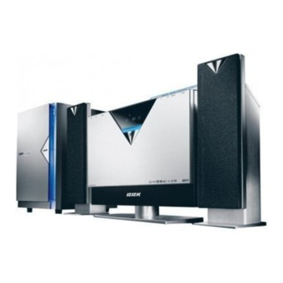
- Page 1 SERVICE MANUAL ABS551T...
-
Page 2: Table Of Contents
CONTENTS SAFETY PRECAUTIONS PREVENTION OF ELECTRO STATIC DISCHARGE(ESD)TO ELECTROSTATICALLY SENSITIVE(ES)DEVICES CONTROL BUTTON LOCATIONS AND EXPLANATIONS PREVERTION OF STATIC ELECTRICITY DISCHARGE ASSEMBLING AND DISASSEMBLING THE MECHANISM UNIT OPTICAL PICKUP UNIT EXPLOSED VIEW AND PART LIST MISCELLANEOUS ELECTRICAL CONFIRMATION VIDEO OUTPUT (LUMINANCE SIGNAL) CONFIRMATION VIDEO OUTPUT(CHROMINANCE SIGNAL) CONFIRMATION MPEG BOARD CHECK WAVEFORM MT1389... -
Page 3: Safety Precautions
1. SAFETY PREAUTIONS 1.1 GENERAL GUIDELINES 1. When servicing, observe the original lead dress. if a short circuit is found, replace all parts which have been overheated or damaged by the short circuit. 2. After servicing, see to it that all the protective devices such as insulation barrier, insulation papers shields are properly installed. -
Page 4: Control Button Locations And Explanations
Front panel illustration POWER button Channel Switch Button 10 11 12 VOL- button VOL+ button Display window IR sensor OPEN/CLOSE button FUNCTION button PLAY/STOP button BAND button PREV button TUNING<< button NEXT button TUNING>> button Glass Rear panel illustration Video out terminal Coaxial out terminal for digital audio External audio in terminal 1 S-video... -
Page 5: Prevertion Of Static Electricity Discharge
4.PREVENTION OF STATIC ELECTRICITY DISCHARGE The laser diode in the traverse unit (optical pickup)may brake down due to static electricity of clothes or human body. Use due caution to electrostatic breakdown when servicing and handling the laser diode. 4.1.Grounding for electrostatic breakdown prevention Some devices such as the DVD player use the optical pickup(laser diode)and the optical pickup will be damaged by static electricity in the working environment.Proceed servicing works under the working environment where grounding works is completed. -
Page 6: Assembling And Disassembling The Mechanism Unit
5. Assembling and disassembling the mechanism unit... -
Page 7: Optical Pickup Unit Explosed View And Part List
OPTICAL PICKUP UNIT EXPLOSED VIEW AND PART LIST... -
Page 10: Miscellaneous
5.2 MISCELLANEOUS 5.2.1 Protection of the LD(Laser diode) Short the parts of LD circuit pattern by soldering. 5.2.2 Cautions on assembly and adjustment Make sure that the workbenches,jigs,tips,tips of soldering irons and measuring instruments are grounded,and that personnel wear wrist straps for ground. Open the LD short lands quickly with a soldering iron after a circuit is connected. -
Page 11: Electrical Confirmation
6.Electrical Confirmation 6.1. Video Output (Luminance Signal) Confirmation DO this confirmation after replacing a P.C.B. Measurement point Mode Disc Color bar 75% DVDT-S15 Video output terminal PLAY(Title 46):DVDT-S15 PLAY(Title 12):DVDT-S01 DVDT-S01 Measuring equipment,tools Confirmation value 200mV/dir,10 sec/dir 1000mVp-p±30mV Purpose:To maintain video signal output compatibility. 1.Connect the oscilloscope to the video output terminal and terminate at 75 ohms. -
Page 12: Video Output(Chrominance Signal) Confirmation
6.2 Video Output(Chrominance Signal) Confirmation Do the confirmation after replacing P.C.B. Measurement point Mode Disc Color bar 75% DVDT-S15 Video output terminal PLAY(Title 46):DVDT-S15 PLAY(Title 12):DVDT-S01 DVDT-S01 Measuring equipment,tools Confirmation value Screwdriver,Oscilloscope 200mV/dir,10 sec/dir 621mVp-p±30mV Purpose:To maintain video signal output compatibility. 1.Connect the oscilloscope to the video output terminal and terminate at 75 ohme. -
Page 13: Mpeg Board Check Waveform
7.MPEG BOARD CHECK WAVEFORM 7.1 27MHz WAVEFORM DIAGRAM 7.2 IC TEA1523 PIN.8 WAVEFORM DIAGRAM... -
Page 14: Mt1389
8.2 MT1389 MT1389 Progressive-Scan DVD Player SOC Specifications are subject to change without notice MediaTek MT1389 is a DVD player system-on-chip (SOC) which incorporates advanced features like high quality TV encoder and state-of-art de-interlace processing. The MT1389 enables consumer electronics manufacturers to build high quality, cost-effective DVD players, portable DVD players or any other home entertainment audio/video devices. - Page 15 MT1389 PRELIMINARY, SUBJECT TO CHANGE WITHOUT NOTICE MTK CONFIDENTIAL, NO DISCLOSURE General Feature List 1024-bytes on-chip RAM Super Integration DVD player single chip Up to 4M bytes FLASH-programming interface High performance analog RF amplifier Supports 5/3.3-Volt. FLASH interface Servo controller and data channel processing Supports power-down mode MPEG-1/MPEG-2/JPEG video Supports additional serial port...
- Page 16 MT1389 PRELIMINARY, SUBJECT TO CHANGE WITHOUT NOTICE MTK CONFIDENTIAL, NO DISCLOSURE Audio Effect Processing TV Encoder Dolby Digital (AC-3)/EX decoding Six 108MHz/12bit DACs DTS/DTS-ES decoding Support NTSC, PAL-BDGHINM, PAL-60 MLP decoding for DVD-Audio Support 525p, 625p progressive TV format MPEG-1 layer 1/layer 2 audio decoding Automatically turn off unconnected channels MPEG-2 layer1/layer2 2-channel audio Support PC monitor (VGA)
-
Page 17: Am29Lv160D
8.3 Am29LV160D 16 Megabit (2 M x 8-Bit/1 M x 16-Bit) CMOS 3.0 Volt-only Boot Sector Flash Memory DISTINCTIVE CHARACTERISTICS Single power supply operation Embedded Algorithms — Full voltage range: 2.7 to 3.6 volt read and write — Embedded Erase algorithm automatically operations for battery-powered applications preprograms and erases the entire chip or any combination of designated sectors... - Page 18 PRODUCT SELECTOR GUIDE Family Part Number Am29LV160D Speed Option Voltage Range: V = 2.7–3.6 V -120 Max access time, ns (t Max CE# access time, ns (t Max OE# access time, ns (t Note: See “AC Characteristics” for full specifications. BLOCK DIAGRAM –...
- Page 19 CONNECTION DIAGRAMS BYTE# DQ15/A-1 DQ14 DQ13 DQ12 Standard TSOP RESET# DQ11 RY/BY# DQ10 BYTE# DQ15/A-1 DQ14 DQ13 DQ12 RESET# Reverse TSOP DQ11 RY/BY# DQ10...
- Page 20 CONNECTION DIAGRAMS RESET# BYTE# DQ15/A-1 DQ14 DQ13 DQ10 DQ12 DQ11 FBGA Top View, Balls Facing Down BYTE# DQ15/A-1 DQ14 DQ13 RESET# DQ12 RY/BY# DQ10 DQ11 Special Handling Instructions Flash memory devices in FBGA packages may be damaged if exposed to ultrasonic cleaning methods. Special handling is required for Flash Memory products The package and/or data integrity may be compromised in FBGA packages.
- Page 21 PIN CONFIGURATION LOGIC SYMBOL A0–A19 = 20 addresses DQ0–DQ14 = 15 data inputs/outputs A0–A19 16 or 8 DQ15/A-1 = DQ15 (data input/output, word mode), DQ0–DQ15 A-1 (LSB address input, byte mode) (A-1) BYTE# = Selects 8-bit or 16-bit mode = Chip enable = Output enable = Write enable RESET#...
-
Page 22: Hy57V641620Hg
HY57V641620HG 4 Banks x 1M x 16Bit Synchronous DRAM 8.4 HY57V641620HG DESCRIPTION The Hyundai HY57V641620HG is a 67,108,864-bit CMOS Synchronous DRAM, ideally suited for the main memory applications which require large memory density and high bandwidth. HY57V641620HG is organized as 4banks of 1,048,576x16. HY57V641620HG is offering fully synchronous operation referenced to a positive edge of the clock. - Page 23 HY57V641620HG PIN CONFIGURATION DQ15 DQ14 DQ13 DQ12 DQ11 DQ10 54pin TSOP II 400mil x 875mil 0.8mm pin pitch LDQM UDQM /CAS /RAS A10/AP PIN DESCRIPTION PIN NAME DESCRIPTION The system clock input. All other inputs are registered to the SDRAM on the Clock rising edge of CLK Controls internal clock signal and when deactivated, the SDRAM will be one...
- Page 24 HY57V641620HG FUNCTIONAL BLOCK DIAGRAM 1Mbit x 4banks x 16 I/O Synchronous DRAM Self refresh logic Internal Row & timer counter 1Mx16 Bank 3 1Mx16 Bank 2 Row active Decoders 1Mx16 Bank 1 1Mx16 Bank 0 Memory refresh Cell Array Column Column Active UDQM...
-
Page 25: Schematic & Pcb Wiring Diagram
9. SCHEMATIC & PCB WIRING DIAGRAM SCHEMATIC & PCB WIRING DIAGRAM FRONT SCHEMATIC DIAGRAM... - Page 26 FRONT SCHEMATIC DIAGRAM...
- Page 27 SUBSIDIARY OUTPUT BOARD...
- Page 28 SUBSIDIARY OUTPUT BOARD...
- Page 29 OUTPUT BOARD SCHEMATIC DIAGRAM...
- Page 30 OUTPUT BOARD SCHEMATIC DIAGRAM...
- Page 31 MIAN SCHEMATIC DIAGRAM...
- Page 34 MIAN SCHEMATIC DIAGRAM...
-
Page 42: Spare Parts List
10. SPARE PARTS LIST ABS551T MATERIAL LIST 1. AV BOARD MATERIAL CODE MATERIAL NAME SPECIFICATIONS UNIT QUANTIT LOCATION 90001 SMD RESISTOR R707~R712 1/16W 0Ω ±5% 0603 0090002 SMD RESISTOR 1/16W 2.2Ω ±5% 0603 R706 0310044 SMD CAPACITOR 50V 33P ±5% NPO 0603... - Page 43 0260198 CD11C 50V10U±20%5×7 2 TC402 0260196 CD11C 16V10U±20%4×7 1.5 TC405,TC406 0700007 SMD DIODE 1N4148 VD401~VD403 0700001 SMD DIODE LS4148 VD401~VD403 700002 SMD DIODE LL4148 VD401~VD403 0700056 SMD DUAL DIODE MMBD4148SE SOT-23 D401~D416 0700148 SMD VOLTAGE REGULATOR DIODE 3.3V ±5% 1/2W ZD401 0700004 SMD VOLTAGE REGULATOR DIODE 5.1V ±5% 1/2W...
- Page 44 6. AI OF POWER AMPLIFIER BOARD MATERIAL CODE MATERIAL NAME SPECIFICATIONS UNIT QUANTIT LOCATION 01564002 4SW1000B-1 R410,R411,R418,R422,R423, 00000229 CARBON FILM RESISTOR 1/6W1K±5% R425 5800099 VOLTAGE REGULATOR DIODE 9.1V ±5% 1/2W VD411 00000269 CARBON FILM RESISTOR 1/6W2K±5% R400,R401,R445 00003609 CARBON FILM RESISTOR 1/6W 7.5K±5% R416,R438 R405,R429,R440,R442,R402,...
- Page 45 2100003 CONNECTION CORDS W1,W2 Φ0.6 SHAPED 7.5mm 6P180 2.5 2PLUG 5P SCREEN- 2150233 FLAT CABLE XS200 SHIELDED WITH L NEEDLE 1563697 2SW1000K-0 9. POWER INDICATOR LIGHT BOARD OF SUBWOOFER MATERIAL CODE MATERIAL NAME SPECIFICATIONS UNIT QUANTIT LOCATION 3P500 2.5 2PLUG WITH L NEEDLE 2121746 FLAT CABLE XP01...
- Page 46 R206,R207,R208,R252,R286, R309,R311,R313,R314,R339, R342,R343,R2109,R2142,R2 143,R2160,R2161,R2163,R21 0090023 SMD RESISTOR 1/16W 10K ±5% 0603 64,R2167,R2187,R2188,R219 9,R259,R260,R2190~R2193, R2198,R2194~R2197,R2107, R2108,R2113 R220,R221,R282,R2185,R22 0090187 SMD RESISTOR 1/16W 12K ±5% 0603 5,R226,R253,R2225 0090024 SMD RESISTOR 1/16W 15K ±5% 0603 R209,R223 0090188 SMD RESISTOR 1/16W 18K ±5% 0603 R210 R211,R312,R315,R316,R212 90025 SMD RESISTOR...
- Page 47 C207,C211,C214,C216,C217, C224,C226~C230,C232,C234 ~C239,C241~C254,C256~C2 59,C267,C268,C270,C271,C2 73,C274,C279,C281~C283,C 289,C291,C294,C297,C301~ 310207 SMD CAPACITOR 50V 104 ±20% X7R 0603 C303,C305,C309,C311~C316 ,C2104,C2119,C2121,C2127, C2138,C2145,C2146,C2152, C2153,C2160,C2162~C2176, C2178,C2140,C2109,C2110, C287,C288 0310362 SMD CAPACITOR 16V 474 +80%-20% Y5V 0603 C218 C201~C204,C221,C240,C217 9,C208,C209,C277,C280,C31 0310234 SMD CAPACITOR 16V 105 +80%-20% Y5V 0603 7,C318,C2154,C319,C320,C2 85,C286,C333,C334,TC242 390355 SMD INDUCTOR...
- Page 48 0881456 SAA6588 SO20 U204 881263 PCM1801U SOP U210 0960226 CRYSTAL OSCILLATOR 4.332MHz 49-s X202 0960020 CRYSTAL OSCILLATOR 27.00MHz 49-S X201 0960019 CRYSTAL OSCILLATOR 12.00MHz 49-S X203 14P 1.0mm STRAIGHT DUAL LINE 1940140 CABLE SOCKET XS204 PLUG 13P 1.0mm STRAIGHT DUAL LINE 1940120 CABLE SOCKET XS206...
Need help?
Do you have a question about the ABS551T and is the answer not in the manual?
Questions and answers