Table of Contents
Advertisement
Quick Links
SERVICE
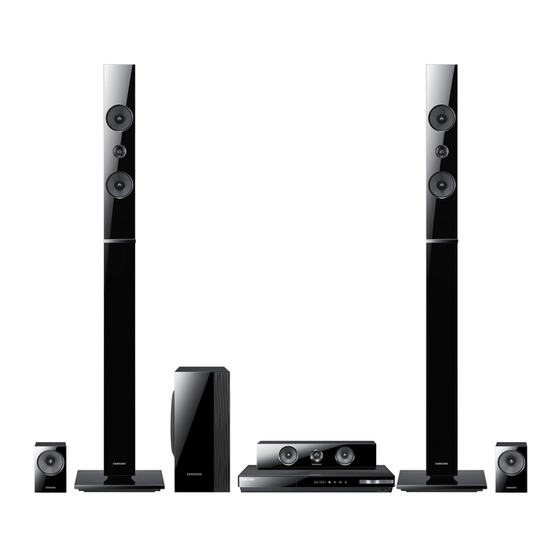
Blu-ray Home Theater System
HT-E5530K
Refer to the service manual in the GSPN (see the rear cover) for more information.
Blu-ray Home Theater
System
Model Name
Model Code
MANUAL
1. Precaution
2. Product Specification
3. Disassembly and Reassembly
4. Troubleshooting
5. PCB Diagram
6. Schematic Diagram
HT-E5530K
HT-E5530K/RU
Contents
Advertisement
Table of Contents

Related Manuals for Samsung HT-E5530K


Summary of Contents for Samsung HT-E5530K
- Page 1 Blu-ray Home Theater System Model Name HT-E5530K Model Code HT-E5530K/RU SERVICE MANUAL Blu-ray Home Theater System Contents 1. Precaution 2. Product Specification 3. Disassembly and Reassembly 4. Troubleshooting 5. PCB Diagram 6. Schematic Diagram HT-E5530K Refer to the service manual in the GSPN (see the rear cover) for more information.
-
Page 2: Table Of Contents
How to update firmware....................4 − 26 4.2.3. Cold Start Method (Initialize Setup) ................4 − 29 4.3. Buyer-Region Code Setting Method .................... 4 − 30 4.3.1. Inserting the Region Code after replacing the Main PCB ............. 4 − 30 Copyright© 1995-2012 SAMSUNG. All rights reserved. - Page 3 6.14. FLASH MEMORY ........................6 − 17 6.15. FIRENCE POWER JTAG DEBUG ..................... 6 − 18 6.16. F_END_MORTOR DRIVER ..................... 6 − 19 6.17. F_END_SC7300........................6 − 20 6.18. SMPS ............................ 6 − 21 Copyright© 1995-2012 SAMSUNG. All rights reserved.
-
Page 4: Precaution
TES T ALL EXPO S ED METAL SU RFACES 2-WIRE CORD ALSO TES T WITH PLUG REVER S ED (US ING AC EARTH ADAPTER P LUG GROUND AS R EQ UIRED) Figure 1.1 AC Leakage Test Copyright© 1995-2012 SAMSUNG. All rights reserved. - Page 5 A replacement part that does not have the same safety characteristics as the original might create shock, fire or other hazards. Copyright© 1995-2012 SAMSUNG. All rights reserved.
-
Page 6: Servicing Precautions
CAUTION First read the “Safety Precautions” section of this manual. If some unforeseen circumstance creates a conflict between the servicing and safety precautions, always follow the safety precautions. Copyright© 1995-2012 SAMSUNG. All rights reserved. -
Page 7: Precautions For Electrostatically Sensitive Devices (Esds)
8) Minimize body motions when handling unpackaged replacement ESDs. Motions such as brushing clothes together, or lifting a foot from a carpeted floor can generate enough static electricity to damage an ESD. Copyright© 1995-2012 SAMSUNG. All rights reserved. -
Page 8: Product Specification
Still Mode BD Wise Picture Control • 3D Sound • HDMI 1.4 with ARC (support HDMI 2 In ) • 2 HDMI In • DLNA • Smart Hub • Allshare • Disc to Digital Copyright© 1995-2012 SAMSUNG. All rights reserved. -
Page 9: Specifications
20 Hz ~ 20 kHz (± 3 dB) Frequency response Digital input 20 Hz ~ 40 kHz (± 4 dB) Amplifier 70 dB S/N Ratio Channel separation 60 dB Input sensitivity (AUX) 500 mV Copyright© 1995-2012 SAMSUNG. All rights reserved. - Page 10 NOTE • Network speeds equal to or below 10 Mbps are not supported. • Samsung Electronics Co., Ltd reserves the right to change the specifications without notice. • Weight and dimensions are approximate. • Design and specifications are subject to change without prior notice.
-
Page 11: Ht-E5Xxx Specifications
20 Hz ~ 20 kHz (± 3 dB) Amplifier Frequency response Digital input 20 Hz ~ 40 kHz (± 4 dB) S/N Ratio 70 dB Channel separation 60 dB Input sensitivity (AUX) 500 mV Copyright© 1995-2012 SAMSUNG. All rights reserved. - Page 12 Subwoofer : 200 x 390 x 350 mm / 6.61 x 13.78 x 11.22 inches Front : 10.4 kg/ 8.59 Ibs Surround : 6.1 kg / 1.37 Ibs Weights Center : 8.8 kg / 1.98 Ibs Subwoofer : 5.5 kg / 8.06 Ibs Copyright© 1995-2012 SAMSUNG. All rights reserved.
- Page 13 NOTE • Network speeds equal to or below 10 Mbps are not supported. • Samsung Electronics Co., Ltd reserves the right to change the specifications without notice. • Weight and dimensions are approximate. • Design and specifications are subject to change without prior notice.
-
Page 14: Specifications Analysis
Ready (EU) / Built-In (Others) Wi-Fi LAN Dongle 2 Inputs 2 Inputs (Exclude U.S., Canada) HDMI IN BACKEND Firenze BACKEND Firenche Main ↔ Loader + Frontend Sunext + Frontend Raptor O : Feature Included X : Not Included Copyright© 1995-2012 SAMSUNG. All rights reserved. -
Page 15: Disk And Format Compatibility
Information about the discs is written in detail on the disc box. Please refer to this if necessary. • When you play a BD-J title, loading may take longer than a normal title or some functions may perform slowly. Copyright© 1995-2012 SAMSUNG. All rights reserved. -
Page 16: Disc Types Your Product Cannot Play
• Samsung cannot guarantee that this product will play every disc bearing the Blu-ray Disc, DVD or CD logo because disc formats evolve, and problems and errors may occur during the creation of Blu-ray Disc, DVD, and CD software and/or the manufacture of discs. -
Page 17: Region Code
Russia, Eastern Europe, India, most of Africa, North Korea, Mongolia China NOTE • If the Region number of a Blu-ray Disc/DVDs does not correspond to the Region number of this product, the product cannot play the disc. Copyright© 1995-2012 SAMSUNG. All rights reserved. 2-10... -
Page 18: Logos Of Discs The Product Can Play
2.5. Logos of Discs the product can play Blu-ray Disc 3D Blu-ray Disc BD-LIVE Dolby DivX NTSC broadcast system in PAL broadcast system in U.S.A, Canada, Korea, Japan U.K, France, Germany, etc. Java 2-11 Copyright© 1995-2012 SAMSUNG. All rights reserved. -
Page 19: Supported Formats
6 ~ 30 SP/ASP H.264 1920 x 1080 6 ~ 30 BP/MP/HP *.3gp 3GPP MPEG4 1920 x 1080 6 ~ 30 SP/ASP MPEG2 1920 x 1080 24/25/30 *.vro MPEG MPEG1 1920 x 1080 24/25/30 LPCM Copyright© 1995-2012 SAMSUNG. All rights reserved. 2-12... - Page 20 Normal playback is not guaranteed if the file’s container information is wrong or the file itself is corrupted. • Files having higher bit or frame rates than standard may stutter when played back. 2-13 Copyright© 1995-2012 SAMSUNG. All rights reserved.
-
Page 21: Accessories
2. Product Specification 2.6. Accessories 2.6.1. Supplied Accessories Accessories Item Item code Remark Remote Control AH59-02407A Ferrite Core 3301-000144 Batteries (AAA size) 4301-000116 Local Samsung Dealer Video Cable AH39-40001V FM Antenna AH42-00021A User Manual AH68-02438H Copyright© 1995-2012 SAMSUNG. All rights reserved. 2-14... -
Page 22: Disassembly And Reassembly
Slide the COVER-TOP back to remove. Pull and lift up COVER-TOP rear side. CAUTION Be careful not to make any scratches as you remove them. Disconnect the FPC cable between the COVER-FRONT ASSY and the MAIN PCB. Copyright© 1995-2012 SAMSUNG. All rights reserved. - Page 23 Description Description Photo 1) Loosen the bottom and side clips and tilt up. 2) Lift the COVER-FRONT at a 45 degree angle upward. then the hooks on the top side can be automatically removed. Copyright© 1995-2012 SAMSUNG. All rights reserved.
- Page 24 Disconnect the DECK cable from the MAIN-PCB. Unfasten the screws of 4 points around the. : BH,+,-,B,M3,L6,ZPC(WHT),SWRCH18A,RF Remove the DECK from the COVER-BOTTOM. For WiI-Fi, unfasten 1 connector to MAIN ASSY and 1 screw. : BH,+,-,B,M3,L6,ZPC(WHT),SWRCH18A,RF Copyright© 1995-2012 SAMSUNG. All rights reserved.
- Page 25 Unplug the FAN cable connected to the main board and then remove the main board from the case. Before pull out the SMPS PCB, Unplug the connector. For SMPS, PCB unfasten 4 screws on bottom-side. : BH,+,-,B,M3,L6,ZPC(WHT),SWRCH18A,RF Copyright© 1995-2012 SAMSUNG. All rights reserved.
-
Page 26: Troubleshooting
4. Troubleshooting 4. Troubleshooting 4.1. Checkpoints by Error Mode Oscilloscope Setting Values Normal Voltage 24 MHz 32.768 KHz Voltage/DIV 1 V/div 200 mV/div 500 mV/div TIME/DIV 100 ms/div 100 ns/div 100 us/div Copyright© 1995-2012 SAMSUNG. All rights reserved. -
Page 27: No Power
1, 2, 4, 5 → OK or S MP S P CB. (means not sh ort)? Re fe r to wa ve pa tter n ima ge of Fig. 4-4. Re place S MP S P CB. Copyright© 1995-2012 SAMSUNG. All rights reserved. - Page 28 VSEN SE CM828 CM828 VSNS VSNS CM829 CM829 GND_01_S GND_01_S 22 NF 22 NF 50 V 50 V RM833 RM833 * 6.18. S MP S * 5.6. S MP S P CB Top <Fig. 4-1> Copyright© 1995-2012 SAMSUNG. All rights reserved.
- Page 29 GND_0 1_S 22NF 22NF RM833 RM833 CM831 CM831 RM840 RM840 30KOHM 30KOHM CM830 CM830 62KOHM 62KOHM 1/10W 1/10W 1/10W 1/10W * 6.18. S MP S * 5.7. S MP S P CB Bottom <Fig. 4-2> Copyright© 1995-2012 SAMSUNG. All rights reserved.
- Page 30 1N4148 WS 1N4148 WS 18V_VC C_03_P 18V_VC C_03_P 220P F 220P F GND_P GND_P TRA801 TRA801 KTC3875S S-BL KTC3875S S-BL * 6.18. S MP S * 5.6. S MP S P CB Top <Fig. 4-3> Copyright© 1995-2012 SAMSUNG. All rights reserved.
- Page 31 3.3 KOHM 3.3 KOHM TP 6 TP 6 EY82 8 EY82 8 1/1 0W 1/1 0W EY82 6 EY82 6 * 6.18. S MP S * 5.6. S MP S P CB Top <Fig. 4-4> Copyright© 1995-2012 SAMSUNG. All rights reserved.
-
Page 32: No Sound
Cha nge s pe a ke r ja ck. Cha nge MAIN P CB. No so und in a ll ch a nne ls ? Che ck wire less co nne ction o r mico m option. Copyright© 1995-2012 SAMSUNG. All rights reserved. -
Page 33: Disc Loading Error
Fig. 4-5 . Is th e Deck cabl e (be tween MAIN & DECK) Re ins e rt DECK ca ble corre ctly. inserted correct ly? Cha nge the DEC K. Copyright© 1995-2012 SAMSUNG. All rights reserved. - Page 34 R12V_ 2 P_O N P_O N 8E8> 8E8> CN2001 CN2001 127301123K2 127301123K2 * 6.5. DC-DC P OWER C2 00 2 IC2 0 01 IC9 1 * 5.6. S MP S P CB Top <Fig. 4-5> Copyright© 1995-2012 SAMSUNG. All rights reserved.
-
Page 35: Remote Doesn't Work
FRONT PANEL P CB. Re fe r to wa ve pa ttern Ye s ima ge of Fig. 4-6 . Cha nge the powe r of IC23 Pin 7, ch a nge the MAIN P CB. Copyright© 1995-2012 SAMSUNG. All rights reserved. 4-10... - Page 36 V_GND USB5V USB5V ST3 .4 ST3 .4 V_5V V_5V USB- USB- ST3.4V ST3.4V FCON1 FCON1 TDA TCLK TCLK * 6.2. FRONT <Re mote Eye Da ta > * 5.2. FRONT Top <Fig. 4-6> 4-11 Copyright© 1995-2012 SAMSUNG. All rights reserved.
-
Page 37: No Picture (Hdmi)
Fig. 4-9 . Che ck HIC1 pre phe ra l circuit. Che ck HO1 S olde ring sta tus . If a ll is ok, cha nge HIC1. Ye s HDMI ca ble Erro r. Copyright© 1995-2012 SAMSUNG. All rights reserved. 4-12... - Page 38 10D8< 10D8< H0_PWR5 H0_PWR5 HR209 HR20 9 P0_5V P0_5V * 6.11. HDMI OUT_RX HCN 1 HCN 2 HCN 2 <HDMI EYE S IGNAL> HIC1 * 5.4 . MAIN P CB Top <Fig. 4-7> 4-13 Copyright© 1995-2012 SAMSUNG. All rights reserved.
- Page 39 SELDECTED RPT'S 1KOHM 1KOHM H1_PWR5 H1_PWR5 HR145 HR145 * 6.11. HDMI OUT_RX HCN 1 HCN 2 HCN 2 <HDMI EYE S IGNAL> H IC 1 * 5.4 . MAIN P CB Top <Fig. 4-8> Copyright© 1995-2012 SAMSUNG. All rights reserved. 4-14...
- Page 40 CEC_ A CEC_A 10C7< 10C7< RCLAMP0504F RCLAMP0504F TX5V TX5V * 6.11. HDMI OUT_RX HCN 1 <AC Le ve l 300 ~ 500 mV> HIC1 * 5.4 . MAIN P CB Top <Fig. 4-9> 4-15 Copyright© 1995-2012 SAMSUNG. All rights reserved.
-
Page 41: No Logo (Hdmi)
Ch an ge MAIN PCB o r Check IC29’s crystal(X2) Syst em MICOM. signal is OK? Re fe r to wa ve pa ttern ima ge of Fig. 4-1 1. HDMI Cable Error. Copyright© 1995-2012 SAMSUNG. All rights reserved. 4-16... - Page 42 10F11<> 10F11<> 10C3< 10C3< CEC_ A CEC_A 10C7< 10C7< RCLAMP0504F RCLAMP0504F TX5V TX5V * 6.11. HDMI OUT_RX HCN 1 <HDMI EYE S IGNAL> HIC1 * 5.4 . MAIN P CB Top <Fig. 4-10> 4-17 Copyright© 1995-2012 SAMSUNG. All rights reserved.
- Page 43 VSSA3 VSSA3 o_AY_HDMITX_TX0P o_AY_HDMITX_TX0P * 6.11. HDMI OUT_RX CN7 0 3 <X2 Must be 24 MHz> IC29 CN9 5 C N 1 * 5.4 . MAIN P CB Top <Fig. 4-11> Copyright© 1995-2012 SAMSUNG. All rights reserved. 4-18...
-
Page 44: No Logo (Composite)
Vide o output from IC19 P in 4? proble m, cha nge the MAIN P CB. Re fe r to wa ve pa ttern ima ge of Fig. 4-1 3. Compone nt Ca ble Error. 4-19 Copyright© 1995-2012 SAMSUNG. All rights reserved. - Page 45 DGND * 6.6. AUDIO/VIDEO/IP OD OUT CEC TEST TEST C847 CN7 0 3 <C847 Compos it Color Ba r> IC29 CN9 5 C N 1 * 5.4. MAIN P CB Top <Fig. 4-12> Copyright© 1995-2012 SAMSUNG. All rights reserved. 4-20...
- Page 46 BIAS BIAS 220NH 220NH DGND DGND OP TION OP TION UNDEFINED UNDEFINED DGND DGND * 6.6. AUDIO/VIDEO/IP OD OUT CEC <Composit Color Ba r> IC29 * 5.4. MAIN P CB Top <Fig. 4-13> 4-21 Copyright© 1995-2012 SAMSUNG. All rights reserved.
-
Page 47: Disc Skips Or Freezing
BD : ov e r 400 mV Cha nge the DECK. DVD : ove r 200 mV CD : ove r 200 mV Cha nge the MAIN P CB. Cha nge the MAIN P CB. Copyright© 1995-2012 SAMSUNG. All rights reserved. 4-22... -
Page 48: No Disc Reading Error
Samsu ng Ele ctronics . which is av a ila ble on the S a m- su ng We b S ite Ye s Update with the new version and try again. 4-23 Copyright© 1995-2012 SAMSUNG. All rights reserved. -
Page 49: Network Error
The connection between LAN and SET is direct. So there is no need to check H/W if there is network problem. If it is, the problem is MAIN CHIP (IC1)'s BGA soldering problem. It must be changed to a new board. Copyright© 1995-2012 SAMSUNG. All rights reserved. 4-24... -
Page 50: Initialization & Upgrade Methods
Region : BD region code / DVD region code Macrovision : Macrovision version Model : Model name Main Touch IC : touch key firmware HDMI RX : HDMI Firmware (Only for HT-E5500 series) 4-25 Copyright© 1995-2012 SAMSUNG. All rights reserved. -
Page 51: How To Update Firmware
The upgrade is complete when the product turns off, and then turns on again by itself. Never turn the product off or back on manually during the update process. Samsung Electronics shall take no legal responsibility for product malfunction caused by an unstable Internet connection or consumer negligence during a software upgrade. - Page 52 8) Select By Disc. NOTE When the system upgrade is done, check the software details in the software Upgrade menu. Do not turn off the product during the Software Upgrade. It may cause the product malfunction. 4-27 Copyright© 1995-2012 SAMSUNG. All rights reserved.
- Page 53 If it downloads new upgrade software, the product will ask you if you want to install it when you turn the product on. NOTE To use the Download in Standby Mode function, your product must be connected to the Internet. Copyright© 1995-2012 SAMSUNG. All rights reserved. 4-28...
-
Page 54: Cold Start Method (Initialize Setup)
3) Then, VFD sign : “INIT” → Power will be turned off automatically. 4) System Micom Cold Start : During Stand-By, just press the Stop Button "■” of remote-controller for over 5 seconds. Then, VFD sign : "RESET". 4-29 Copyright© 1995-2012 SAMSUNG. All rights reserved. -
Page 55: Buyer-Region Code Setting Method
NOTE The “T-MODE” indicator on the VFD only appears for a very short time. 3) You can see “TEST − −” on the VFD. Insert the number “46” to select the Region Code. Copyright© 1995-2012 SAMSUNG. All rights reserved. 4-30... - Page 56 “000” and the region is USA which supports 5.1CH Audio output. If it is “047EU2”, it means that you inserted region code “047” and the region is Europe which supports 2.1ch Audio output. 4-31 Copyright© 1995-2012 SAMSUNG. All rights reserved.
- Page 57 SINGPORE, VIETNAM(XS), INDONESIA(XD), MALAYSIA(XM), THAILAND(XT), INDIA(XL) RUSSIA, UKRAINE, KAZAKHSTAN(RU) AUSTRALIA, NEWZILAND(XY) ARAB, PAKISTAN, EGYPT, IRAQ, LEBANON, SYLBIA, MOROCCO, TUNIS(ZN), SAUDI(UM), ALGERIA(SH), S.AFRICA(XA), ISRAEL(SQ), NIGERIA(SW), SUDAN(SJ), ETIOPIA, KENYA(KE) CHINA(XZ), HONGKONG(ZK) BRAZIL(ZD) CANADA(ZC) IRAN(HC) ETC1 ETC2 ETC3 Copyright© 1995-2012 SAMSUNG. All rights reserved. 4-32...
- Page 58 SINGPORE, VIETNAM(XS), INDONESIA(XD), MALAYSIA(XM), THAILAND(XT), INDIA(XL) RUSSIA, UKRAINE, KAZAKHSTAN(RU) AUSTRALIA, NEWZILAND(XY) ARAB, PAKISTAN, EGYPT, IRAQ, LEBANON, SYLBIA, MOROCCO, TUNIS(ZN), SAUDI(UM), ALGERIA(SH), S.AFRICA(XA), ISRAEL(SQ), NIGERIA(SW), SUDAN(SJ), ETIOPIA, KENYA(KE) CHINA(XZ), HONGKONG(ZK) BRAZIL(ZD) CANADA(ZC) IRAN(HC) ETC1 ETC2 ETC3 4-33 Copyright© 1995-2012 SAMSUNG. All rights reserved.
-
Page 59: Pcb Diagram
T_RESET T_RES ET MIC IN MIC SIG G ND AVG ND MIC SEN MIC SEN MIC DATA MIC DATA MIC CLK MIC CLK G ND AVG ND TACT TACT 28 G ND DG ND Copyright© 1995-2012 SAMSUNG. All rights reserved. -
Page 60: Front Pcb Top
5. PCB Diagram 5.2. FRONT PCB Top KIC1 VC N 5 TP 1 FCON1 KC N 1 KC N 2 US C N1 Copyright© 1995-2012 SAMSUNG. All rights reserved. -
Page 61: Pin Connection
MIC DATA MIC SEN AVGND MIC SIG T_RESET VFD CLK VFD DATA VFD CE VGND VFD12V_PW VFD12V_PW VGND DGND ST3.4V REMOT BUZZER DGND Touch Key DATA Touch Key CLK USB+ USB - USB5V USB5V Copyright© 1995-2012 SAMSUNG. All rights reserved. -
Page 62: Test Point Wave Form
5. PCB Diagram 5.2.2. Test Point Wave Form Copyright© 1995-2012 SAMSUNG. All rights reserved. -
Page 63: Front Pcb Bottom
5. PCB Diagram 5.3. FRONT PCB Bottom VIC 1 Copyright© 1995-2012 SAMSUNG. All rights reserved. -
Page 64: Main Pcb Top
IC2 9 ZIC 20 03 IC2002 IC2001 IC23 CN95 IC17 CN 1 C N 4 C N 2 5 IC 9 1 IC801 B C N 1 C N 2 C N 2 2 Copyright© 1995-2012 SAMSUNG. All rights reserved. -
Page 65: Pin Connection
VFD CE SLO2+ VFD DATA SLO2- VFD CLK BD RF- T_RESET BD RF+ MIC IN VREF_1.65V VCC_5V MIC SEN VREF_2.1V MIC DATA DVD_PD_FSW MIC CLK BD_PD_FSW PU_SEL TACT BD MPD DVD_VR DVD_MPD CD_VR DVD LD Copyright© 1995-2012 SAMSUNG. All rights reserved. - Page 66 5. PCB Diagram 6) CN2001 MAIN Power Connector Pin No. Signal DGND R12V P_ON DGND D12V_PW D12V_PW D12V_PW DGND DGND ST3.4V ST3.4V VARI_SMPS R12V PGND PGND PGND PGND PGND +35V +35V +35V +35V +35V Copyright© 1995-2012 SAMSUNG. All rights reserved.
-
Page 67: Test Point Wave Form
5. PCB Diagram 5.4.2. Test Point Wave Form Copyright© 1995-2012 SAMSUNG. All rights reserved. -
Page 68: Main Pcb Bottom
5. PCB Diagram 5.5. MAIN PCB Bottom 5-10 Copyright© 1995-2012 SAMSUNG. All rights reserved. -
Page 69: Smps Pcb Top
5. PCB Diagram 5.6. SMPS PCB Top CN801 CN802 Copyright© 1995-2012 SAMSUNG. All rights reserved. 5-11... -
Page 70: Smps Pcb Bottom
5. PCB Diagram 5.7. SMPS PCB Bottom 5-12 Copyright© 1995-2012 SAMSUNG. All rights reserved. -
Page 71: Schematic Diagram
RX Mod u le ITO FILM 2Gb (128 M x 16) (128 M x 16 ) 2Gb (128 M x 16 ) (768) G Byte Tu n er CS53 46 MIC/AS C SMP S TION) POW ER Copyright© 1995-2012 SAMSUNG. All rights reserved. -
Page 72: Front
MICIN2 MICIN2 KCN2 KCN2 40000O HM 40000O HM DGND DGND 40000OHM 40000OHM 40000OHM 40000OHM KBD4 KBD4 1/10W 1/10W UGND UGND DGND DGND 1KOHM 1KOHM AVGND AVGND KR17 KR17 KBD5 KBD5 AVGND AVGND V_GND V_GND Copyright© 1995-2012 SAMSUNG. All rights reserved. -
Page 73: Test Point Wave Form
6. Schematic Diagram 6.2.1. Test Point Wave Form Copyright© 1995-2012 SAMSUNG. All rights reserved. -
Page 74: Pwm_Variable_Fan
Q20 1 0.01OHM 0.01OHM TP12 02 TP12 02 0.01OHM 0.01OHM 5000MA 5000MA PGND PGND 5000MA 5000MA FGND FGND KRC106S- RTK KRC106S- RTK 12C4> 12C4> VARI_PC_A VARI_PC_A Q20 2 Q20 2 FGND FGND DGND DGND Copyright© 1995-2012 SAMSUNG. All rights reserved. -
Page 75: Power_Amp
PGND DGND DGND PGND PGND 3F10< 3F10< SP K_FL- SP K_FL- 0.01OHM 0.01OHM 1/10W 1/10W 5000MA 5000MA 3.3OHM 3.3OHM BD200 4 BD200 R202 3 R202 3 R202 4 R202 4 3.3OHM 3.3OHM 1/10W 1/10W Copyright© 1995-2012 SAMSUNG. All rights reserved. -
Page 76: Dc-Dc Power
40 V 40 V DGND DGND DGND DGND DGND DGND DGND DGND DGND DGND DGND DGND FE5. 0V_P W FE5. 0V_P W DGND DGND FE5.0V_PW FE5.0V_PW DGND DGND RB05 0LA-40TR RB05 0LA-40TR DGND DGND Copyright© 1995-2012 SAMSUNG. All rights reserved. -
Page 77: Audio/Video/Ipod Out Cec
_AVSS33A 2 p_DAC3CH _AVSS3 3A2 o_D AC3C H_IO2 o_D AC3C H_IO2 220N H 220N H DGND DGND OPTION OPTION UNDEFINED UNDEFINED DGND DGND DGND DGND DGND DGND DGND DGND TEST O PTION TEST O PTION Copyright© 1995-2012 SAMSUNG. All rights reserved. -
Page 78: Test Point Wave Form
6. Schematic Diagram 6.6.1. Test Point Wave Form Copyright© 1995-2012 SAMSUNG. All rights reserved. -
Page 79: Usb/Ethernet
R433 4.7KOHM 4.7KOHM 1/16W 1/16W R434 R434 R428 R428 LED1_AD1 LED1_AD1 R436 R436 4.7KOHM 4.7KOHM 1/16W 1/16W R429 R429 LED0_AD0 LED0_AD0 4.7KOHM 4.7KOHM 1/16 W 1/16W R435 R435 R430 R430 I_MAC_RX_DV I_MAC_RX_DV DGND DGND Copyright© 1995-2012 SAMSUNG. All rights reserved. -
Page 80: Usb Hub_Ipod Certi
1/16W 150MA 150MA MGND1 MGND1 DGND DGND MGND3 MGND3 NEW CP CHIP IS OPT ION NEW CP CHIP IS OPT ION OPTIO N OPTIO N DGND DGND DGND DGND DGND DGND DGND DGND 6-10 Copyright© 1995-2012 SAMSUNG. All rights reserved. -
Page 81: Front Micom
100NF DGND DGND 16 V DGND DGND DGND DGND OPEN OPEN DGND DGND 10022H S- 28C 00 10022H S- 28C 00 DGND DGND FRONT FULL DOWN CHECK FRONT FULL DOWN CHECK DGND DGND Copyright© 1995-2012 SAMSUNG. All rights reserved. 6-11... -
Page 82: Dir/Adc/Rx Switching/D.in
12KOHM OR27 OR27 OR28 OR28 DIG.IN DIG.IN E4500 E4500 ARC IN ARC IN E5300 E5300 DGND DGND DIG.IN DIG.IN E5500 E5500 ARC IN ARC IN HDMI.IN HDMI.IN (HDMI IC SWITCH) (HDMI IC SWITCH) 6-12 Copyright© 1995-2012 SAMSUNG. All rights reserved. -
Page 83: Hdmi Out_Rx
0.01OHM DGND DGND 5000MA 5000MA DGND DGND PLACE ALL DECOUPLING CAPACITORS PLACE ALL DECOUPLING CAPACITORS AS CLOSE TO THE PIN AS P OSSIBLE AS CLOSE TO THE PIN AS P OSSIBLE DGND DGND Copyright© 1995-2012 SAMSUNG. All rights reserved. 6-13... -
Page 84: Test Point Wave Form
6. Schematic Diagram 6.11.1. Test Point Wave Form 6-14 Copyright© 1995-2012 SAMSUNG. All rights reserved. -
Page 85: Ddr3 Interface
VSSQ DDRB_CLK+ DDRB_CLK+ R810 R810 VSSQ VSSQ DDRA_CLK1+ DDRA_CLK1+ VSSQ VSSQ VSSQ VSSQ DGND DGND DDRB_CLK- DDRB_CLK- VSSQ VSSQ DDRA_CLK1- DDRA_CLK1- DGND DGND VSSQ VSSQ VSSQ VSSQ VSSQ VSSQ DGND DGND DGND DGND Copyright© 1995-2012 SAMSUNG. All rights reserved. 6-15... -
Page 86: Interface/Sata Block
R257 4.7 KOHM 4.7 KOHM I_EXTINT1 I_EXTINT1 R259 R259 4.7 KOHM 4.7 KOHM DGND DGND DGND DGND DRM_WP DRM_WP 12C3> 12C3> DRM_SCL DRM_SCL 12B3> 12B3> DGND DGND DRM_SDA DRM_SDA 12 B3<> 12 B3<> 6-16 Copyright© 1995-2012 SAMSUNG. All rights reserved. -
Page 87: Flash Memory
R817 10K OPEN NAND3.3V_PW NAND3.3V_PW R725 OPEN 0 OHM R725 OPEN 0 OHM DGND DGND EMMC_D0 EMMC_D0 EMMC_D1 EMMC_D1 EMMC_D2 EMMC_D2 EMMC_D3 EMMC_D3 EMMC_D4 EMMC_D4 EMMC_D5 EMMC_D5 EMMC_D6 EMMC_D6 EMMC_D7 EMMC_D7 EMMC_CMD EMMC_CMD Copyright© 1995-2012 SAMSUNG. All rights reserved. 6-17... -
Page 88: Firence Power Jtag Debug
6. Schematic Diagram 6.15. FIRENCE POWER JTAG DEBUG 6-18 Copyright© 1995-2012 SAMSUNG. All rights reserved. -
Page 89: F_End_Mortor Driver
LOAD_P P5 V_1 P5 V_1 P5 V12L P5 V12L DRV_DMO DRV_DMO FCS_P FCS_P TRK_N TRK_N FCS_N FCS_N TRK_P TRK_P DRV_LDIN DRV_LDIN DRV_TRO DRV_TRO DRV_FLO DRV_FLO DRV_FRO DRV_FRO DRV_LDIN DRV_LDIN DRV_DMO DRV_DMO DGND DGND Copyright© 1995-2012 SAMSUNG. All rights reserved. 6-19... -
Page 90: F_End_Sc7300
F_EJEC T F_EJEC T OP USE L OP USE L DISC _IN DISC _IN 15E 7> 15E 7> 8A5< 8A5< OP TION OP TION 0OHM 0OHM DGND DGND MIO3 MIO3 DGND DGND DGND DGND 6-20 Copyright© 1995-2012 SAMSUNG. All rights reserved. -
Page 91: Smps
RX801S RX801S 1.5MOHM 1.5MOHM1/2W 1/2W EY803 EY803 LI_AC_P LI_AC_P GND_S GND_S VX801S VX801S INR10D5 61K-TK INR10D5 61K-TK NE_IN_P NE_IN_P FP801S FP801S S R-5-5A S R-5-5A LI_IN_P LI_IN_P EY801 EY801 EY802 EY802 CN801 CN801 Copyright© 1995-2012 SAMSUNG. All rights reserved. 6-21... - Page 92 E.Asia, W.Asia, https://gspn2.samsungcsportal.com China, Japan N.America, S.America https://gspn3.samsungcsportal.com This Service Manual is a property of Samsung Electronics Co.,Ltd. © 2012 Samsung Electronics Co.,Ltd. Any unauthorized use of Manual can be punished under All rights reserved. applicable International and/or domestic law.
Need help?
Do you have a question about the HT-E5530K and is the answer not in the manual?
Questions and answers