Daewoo DQD-2100D Service Manual
Hide thumbs
Also See for DQD-2100D:
- Service manual (63 pages) ,
- Owner's manual (50 pages) ,
- Owner's manual (17 pages)
Table of Contents
Advertisement
Quick Links
S/M No. : VD6100NET0
Service Manual
MODEL :DQD-6100D
DQD-2100D
Caution
: In this Manual, some parts can be changed for improving, their
performance without notice in the parts list. So, if you need the
latest parts information,please refer to PPL(Parts Price List) in
Service Information Center (http://svc.dwe.co.kr).
DAEWOO ELECTRONICS CO., LTD.
http : //svc.dwe.co.kr
Jun. 2002
Advertisement
Table of Contents

Related Manuals for Daewoo DQD-2100D


Summary of Contents for Daewoo DQD-2100D
- Page 1 : In this Manual, some parts can be changed for improving, their performance without notice in the parts list. So, if you need the latest parts information,please refer to PPL(Parts Price List) in Service Information Center (http://svc.dwe.co.kr). DAEWOO ELECTRONICS CO., LTD. http : //svc.dwe.co.kr Jun. 2002...
-
Page 2: Table Of Contents
CONTENTS EXTERNAL VIEWS ......................2 1. FRONT VIEWS ........................2 2. REAR VIEWS..........................2 SPECIFICATIONS ......................3 CIRCUIT DIAGRAM........................4 CIRCUIT OPERATIONAL DESCRIPTION ................13 TROUBLE SHOOTING ......................26 WAVEFORMS..........................36 COMPONENTS LOCATION GUIDE ON PCB BOTTOM VIEW ..........45 DISASSEMBLY .........................47 ELECTRICAL PARTSLIST......................51... -
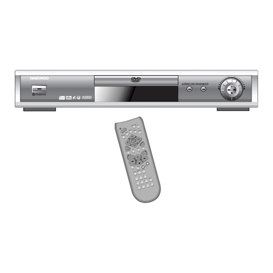
Page 3: External Views
EXTERNAL VIEWS 1. FORNT VIEWS 1)DQD-2100D 2) DQD-6100D 2. REAR VIEWS 1) DQD-2100D AUDIO OUT (2 CH)VIDEO OUT DIGITAL AUDIO OUT EURO AV 2) DQD-6100D AUDIO OUT (5.1 CH) AUDIO OUT (2 CH)VIDEO OUT DIGITAL AUDIO OUT EURO AV... -
Page 4: Specifications
SPECIFICATIONS 1. Prodcut features - Over 500 resolution of horizontal frequency - Disc playback of DVD, VCD, CD, CD-R, CR-RW - Dolby Digital decoding - 5.1ch Analog signal output(6100, 6101) - DTS output - Screen zoom function - Special playback function(slow playback/fast playback) - Component output(Y, Cr, Cb) 2. -
Page 5: Circuit Diagram
CIRCUIT DIAGRAM POWER SUPPLY SCHEMATIC DIAGRAM(DQD-6100,220V) - Page 6 CIRCUIT DIAGRAM VIDEO...
- Page 7 CIRCUIT DIAGRAM AUDIO...
- Page 8 CIRCUIT DIAGRAM VFD/JOG...
- Page 9 CIRCUIT DIAGRAM...
- Page 10 CIRCUIT DIAGRAM VCR_INT(DVD)
- Page 11 CIRCUIT DIAGRAM ATAPI(DVD)
- Page 12 CIRCUIT DIAGRAM CPU-ZR36703(DVD)
- Page 13 CIRCUIT DIAGRAM MPEG DECODER...
-
Page 14: Circuit Operational Description
CIRCUIT OPERATIONAL DESCRIPTION POWER SECTION 1. POWER SUPPLY OPERATION 1) AC input and EMI FILTER AC inlet consists of Line Filter, X-Cap, Y-Cap, Varister. Line Filter(L801, L802), X-Cap(C803, C888), Y-Cap(C801) belong to EMI Filter section. They decrease noise to get into and out of AC Line. - Page 15 CIRCUIT OPERATIONAL DESCRIPTION 3) Sunbber circuit Sunbber circuit protects speedy voltage rising between Collector and Emitter when Main Switching TR is turned off. So Collector and Emitter voltage enter into safety operation and noise is decreased. When TR is turnd off, because high reverse voltage is generated between Collector and Emitter, it is rectified to D802, smoothed to C807 and consumed to R809.
- Page 16 CIRCUIT OPERATIONAL DESCRIPTION 5) Costant-voltage Circuit This circuit maintains constant voltage. When voltage is lower or higher than reference voltage(2.5V) of IC801 pin1, this circuit compensates for a loss. Base voltage of Switching TR is controlled and final voltage is regulated by increasing or decreasing Internal Diode Current of IC801. Picture Costant-voltage Circuit 6) Secondary rectification circuit...
- Page 17 CIRCUIT OPERATIONAL DESCRIPTION 7) Output terminal When power is turned off at power applied status, +3.3V is applied to Q822 Base terminal and Q824 MOS FET outputs MVCC(+5V) to Drain terminal. When power is turned on, low signal(0V) is applied to Q822 Base terminal. At this time, Q824 MOS FET outputs MVCC(+5V) to Drain terminal and +5V to Source terminal.
- Page 18 CIRCUIT OPERATIONAL DESCRIPTION FRONT SECTION 1. VFD DRIVER 1) Overview IC710 implements following functions by serial communication with MICOM depending on the software. * CMOS Technology * Internal Pull-Low Resistance * 4-step Dimming circuitry * Output from 8 to 18 Segment * Output from 7 to 10 Grid * Built-in Noise filter in Serial clock and serial Input Pins with 2MHz sampling * 8-bit x 6 channels Analog-to-Digital Converter with +-3LSB Accuracy...
- Page 19 CIRCUIT OPERATIONAL DESCRIPTION 2. Front Part Operational Description 1) KEY SCAN & FLD Driver Interface 2) Operation Description * If user presses KEY while IC500(ZR36705) implements KEY SCAN using VFD DRIVER(PT6355), the KEY input DATA go to IC500 by SERIAL Communication, then IC500 analyzes and processes the input DATA.
- Page 20 CIRCUIT OPERATIONAL DESCRIPTION AUDIO SECTION 1. 5.1 CH AUDIO DAC IC 1) Overview 24-BIT, 192-kHZ SAMPLING 6-CHANNEL ENHANCED MULTILEVEL DELTA-SIGMA DIGITAL-TO-ANALOG CONVERTER 2) Functions It, as a 5.1CH D/A converter IC, transforms Digital signals to Analog signals by receiving 3 CLOCK (System CLOCK, Shift CLOCK, Left and Right CLOCK) and 3 DATA from MPEG DECODER.
- Page 21 CIRCUIT OPERATIONAL DESCRIPTION 2. 2CH AUDIO DAC IC(IC300) : PCM1748KE 1) Overview 24-BIT, 96-Khz sampling Enhanced multilevel Delta-sigma Digital-to-Analog Converter 2) Functions It, as a 2CH D/A CONVERTER IC, receives 3 CLOCK and 1 DATA from MPEG DECODER and 3 MODE control signal from MICOM, and then outputs Analog signal of L/R Channel.
- Page 22 CIRCUIT OPERATIONAL DESCRIPTION 3. OP-AMP IC (IC303, IC304, IC305) : NJM4580M 1) Overview Dual operational amplifier 2) Functions It amplifies Analog audio signal from D/A Converter IC. Each associates to and amplifies 2 channels, and then outputs 5.1 Channel to JK300. cf) 2CH Audio DAC IC (IC300) model outputs 2 Channels to JK301 using only OP-AMP IC (IC 303).
- Page 23 CIRCUIT OPERATIONAL DESCRIPTION 5. General Audio Operation for 5.1CH 1) Overview It receives CLOCK and DATA from MPEG DECODER(IC405) and transforms Digital signal to Analog signal at AUDIO D/A CONVERTER(IC350) then, amplifies Analog signal (IC303, IC304, IC305)and outputs to 5.1 CH Jack (JK300) and 2CH Jack (JK301). After Noise Filtering Digital signal from MPEG DECODER(IC405) at HEX Inverting Gates IC(IC306), it outputs Digital signal to Coaxial Jack (JK302).
- Page 24 CIRCUIT OPERATIONAL DESCRIPTION MPEG B/D SECTION 1. Operational Description of MPEG B/D 1) General Operation of B/D (1) Initial power supply operation When the power cord is plugged in, only EVER power is outputted to use minimum power supply such as u-COM and Flash Memory and MAIN power input is on standby status.
- Page 25 CIRCUIT OPERATIONAL DESCRIPTION 2. MPEG Decoder : ZR36732(IC 405) 1) Overview Because IC 405(ZR36732) includes Video Encoder function as well as MPEG Decoding function, it outputs Analog Video signal directly from IC. Output signal could be selected as either Composite/S-VHS composition or Composite/Component (Y, Cr, Cb) composition.
- Page 26 CIRCUIT OPERATIONAL DESCRIPTION 3. U-COM: ZR36703(IC 500) 1) Overview IC500 (ZR36703) controls the overall MPEG B/D, and receives DATA from Flash Memory and displays Logo screen, and controls MPEG Decoder to output Video/Audio signal by decoding MPEG format. It also controls OSD display such as Setup related to DVD. 2) Input/Output terminal * Input:It receives DVD MPEG Data inputted from Loader, Data inputted from Memory and interface Data from IC (MPEG Decoder etc.).
-
Page 27: Troubleshooting
TROUBLESHOOTING 1. POWER circuit Caution You must use insulated trance during the first part test of POWER circuit. No POWER POWER cord/fuse is OK? Exchange POWER code/fuse Voltage connected at D801? Check L801,L802 Voltage connected at L804? Check Q801 Switching wave at T801 pin #6,7,8? Check D803,D804,D805 D821, D822, D823, D824, D825,... - Page 28 TROUBLESHOOTING 2. Front Circuits No VFD Letter Display or Broken Letter -15V obtained at F(+), -19.5V at F(-)? Check POWER circuit +5V obtained at IC710 pin #1, #44? Check POWER circuit -24V obtained at IC710 pin #16, #17? Check POWER circuit Input signal obtained at IC710 pin Check communication line with #12, #13, #15?
- Page 29 TROUBLESHOOTING 3. AUDIO circuit Caution Before the AUDIO circuit test, check SETUP MENU setting first by remote controller. A. Analog OUT No AUDIO output from 5.1CH JACK(JK300) In case of 5.1CH setting In case of 2CH setting Is “Digital Output” item in Audio menu in SETUP screen set properly to “Bitstream”...
- Page 30 TROUBLESHOOTING Caution In case of COAXIAL and OPTICAL, check connection with receiver first before the circuit test. B. Digital OUT No AUDIO output from COAXIAL JACK(JK302) RECEIVER is on COAXIAL Change RECEIVER setting MODE? AUDIO DIGITAL signal at P205 Check FFC CABLE connected to P205 and pin #1? MPEG Decoder IC pin #133 Check POWER circuit and +5V...
- Page 31 TROUBLESHOOTING 4. VIDEO circuit Caution Before the VIDEO circuit test, check SETUP MENU setting first by remote controller. No VIDEO output from JK301 yellow TV setting on SETUP MENU is PAL Change setting to PAL mode mode? Check FFC CABLE connected to P205 Is there Video signal from P205 pin #20? and MPEG Decoder IC pin #100-#106 Is there Video signal from...
- Page 32 TROUBLESHOOTING No S-Video output from JK102 TV setting on SETUP MENU is PAL Change setting to PAL mode mode? VIDEO output of SETUP MENU is set on S- Change setting to S-Video Video? Is there Video signal from P205 pin Check FFC CABLE connected to P205 #18,19? and MPEG Decoder IC pin #100-#106...
- Page 33 TROUBLESHOOTING 5. MPEG B/D No LOGO display After checking Power_On_L Signal at Is Power supplied? P505 pin#8, check CPU IC Does Oscillation Device oscillate? Check OS500,OS401 Is Digital Data transmitted from CPU Check Flash Memory and CPU IC and Flash? Is Digital Data transmitted to SDRAM Check MPEG Decoder IC from MPEG Decoder IC?
- Page 34 TROUBLESHOOTING No Digital Audio output Is Digital Data transmitted from CPU and Check Flash Memory and CPU Flash? Is Digital Audio Data transmitted to MPEG Check MPEG Decoder IC Decoder IC pin #133? Is there Audio signal from P481 pin Check FFC CABLE connected to P481 Check Analog B/D...
- Page 35 TROUBLESHOOTING 6. SCART No Audio with SCART Jack (JK103) Is there Audio signal in JK103 Check JK103 and SCART #1 and #3 pin? Cable. Check it with the same method of 2CH Setting of AUDIO circuit(1). No Video with SCART Jack (JK103) Is “TV Type”...
- Page 36 TROUBLESHOOTING No conversion to MODE by pressing SCART button on remote control. Is there voltage change in Q111, Q112 Base like below each time you press SCART button on remote control (Mode Conversion)? (Only when H:3.3V, L:0V) Mode Terminal AV AV Wide TV Q111 Base(TV-CON) Check CABLE connecting with P202 and check Q112 Base(16/9-CON)
-
Page 37: Waveforms
WAVEFORMS 1. MICOM/MPEG KDV-N TEST DVD VIDEO (TITLE1/CHAPTER4) Color Bar 100% • MICOM Serial waveform(IC500, ZR36703) 1) (IC500-7PIN) 0.1s/2V 2) (IC500-22PIN) 0.5 /2V 3) (IC500-23PIN) 0.1s/2V 3.42V , 1.73V/OFF SET 3.42V , 1.73V/OFF SET 3.42V ,1.73V/OFF SET 4) (IC500-87PIN) 20ms/2V 5) (IC500-95PIN) 10ms/2V 3.42V , 1.73V/OFF SET... - Page 38 WAVEFORMS 2. MICOM/MPEG IC, LOADER and Serial SIGNAL(P455) KDV-N TEST DVD VIDEO(TITLE1/CHAPTER4) Color Bar100% 9) (P455-3PIN) 0.5 /2V 10) (P455-4PIN) 0.5 /2V 11) (P455-5PIN) 0.5 /2V 3.19V P, 1.36V/OFF SET 3.19V , 1.36V/OFF SET 3.19V , 1.36V/OFF SET 12) (P455-6PIN) 0.5 /2V 13) (P455-7PIN) 0.5 /2V 14) (P455-8PIN) 0.5 /2V 3.19V...
- Page 39 WAVEFORMS 21) (P455-15PIN) 0.5 /2V 22) (P455-16PIN) 0.5 /2V 23) (P455-17PIN) 0.5 /2V 3.19V , 1.36V/OFF SET 3.19V , 1.36V/OFF SET 3.19V , 1.36V/OFF SET 25) (P455-23PIN) 5ms/1V 24) (P455-18PIN) 0.5 /2V 26) (P455-25PIN) 0.5 /1V 3.19V , 1.36V/OFF SET 2.64V , 2V/OFF SET 3.19V...
- Page 40 WAVEFORMS 3. Serial signal( P205) between DVD B/D and MAIN B/D Optical signal which is output in MPEG • 32) (P205-1PIN) 0.5 /2V 3.28V , 1.66V/OFF SET IC405 - 133PIN (SPDIF-145) • 2CH AUDIO DAC-Mode Contal Signal 33) (P205-2PIN) 20ms/2V 34) (P205-3PIN) 20ms/2V 35) (P205-4PIN) 10ms/2V 3.42...
- Page 41 WAVEFORMS • 2CH/6CH-INPUT DATA SIGNAL • 6CH-INPUT DATA SIGNAL 39) (P205-10PIN) 5 /2V 40) (P205-11PIN) 5 /2V 41) (P205-13PIN) 5 /2V 3.42V/p-p, 1.65V/OFF SET 3.42V/p-p, 1.65V/OFF SET 3.42V/p-p, 1.65V/OFF SET IC405 - 136PIN (ASDAT0) IC405 - 137PIN (ASDAT1) IC405 - 138PIN (ASDAT2) •...
- Page 42 WAVEFORMS • Signal which is OUTPUT from MICOM and INPUT at VFD DRIVE IC 48) (P205-24PIN) 10ms/2V 49) (P205-25PIN) 0.2ms/2V 50) (P205-27PIN) 1ms/2V 3.37V/p-p,1.73V/OFF SET 3.37V/p-p, 1.73V/OFF SET 5.38V/p-p, 2.68V/OFF SET IC500-83PIN (FPSEL) IC500-84PIN (FPCLK) IC500-100PIN (FPDOUT) 4. VFD • VFD DRIVE IC OUTPUT WAVEFORM 51) (IC710-14PIN) 20ms/2V 53) (IC710-18PIN) 2ms/5V 52) (IC710-2,4PIN) 0.5 /0.5V...
- Page 43 WAVEFORMS • OP AMP OUTPUT WAVEFORM 56) (IC303-1PIN)0.5ms/0.5V 57) (IC305-7PIN)0.5ms/200mV 58) (C382 Terminal )0.2ms/50mV 813mV , 5.89V/OFF SET 175mV , 5.89V/OFF SET 34mV , 0V/OFF SET IC303-7PIN -> Noise is almost caught BNC CABLE use IC304-1PIN , 7PIN IC305-1 PIN •...
- Page 44 WAVEFORMS 6. VIDEO OUTPUT KDV-N TEST DVD VIDEO(TITLE2/CHAPTER4) Color Bar 100% • Composite OUTPUT 64) (JK301-yellowPIN) 10 /1V 2.3V/p-p, 0V/OFF SET (CVBS-C) • Component OUTPUT 65) (JK501-blue PIN)10 /0.5V 66) (JK501-red PIN) 10 /0.5V 67) (JK501-green PIN )10 /0.5V 1.72V/p-p, 1.27V/OFF SET 1.72V/p-p, 1.27V/OFF SET 1.95V/p-p, 1.63V/OFF SET (CVBS-G-Y)
- Page 45 WAVEFORMS 6. SCART OUTPUT KDV-N TEST DVD VIDEO(TITLE1/CHAPTER4) Color Bar 100% 1KHz 1KHz -20dB -20dB • AUDIO OUTPUT 70) (JK301-1PIN ) 0.5 /0.2V 71) (JK301-3 PIN) 0.5 /0.2V 292mV/p-p, 0V/OFF SET (AOR) 292mV/p-p, 0V/OFF SET (AOL) • VIDEO OUTPUT 72) (JK103-19 PIN)10 /1V 2V/p-p, 0V/OFF SET •...
-
Page 46: Components Location Guide On Pcb Bottom View
COMPONENTS LOCATION GUIDE ON PCB BOTTOM VIEW... - Page 47 COMPONENTS LOCATION GUIDE ON PCB BOTTOM VIEW J O G M P E G...
-
Page 48: Disassembly
DISASSEMBLY... - Page 49 DISASSEMBLY...
- Page 50 DISASSEMBLY...
- Page 51 DISASSEMBLY...
-
Page 52: Electrical Partslist
ELECTRICAL PARTSLIST C A U T I O N : In this Service Manual, some parts can be changed for improving their performance without notice in the parts list. So, if you need the latest parts information, please refer to PPL(Parts Price List)in Service information Center(http://svc.dwe.co.kr) 1. - Page 53 ELECTRICAL PARTSLIST PATRT-CODE PART-NAME PART-DESC PATRT-CODE PART-NAME PART-DESC C348 HCQK201JBA C CHIP CERA 50V CH 200PF J 1608 R100 HRFS750JBA R CHIP 1/16 75 OHM J 1608 C349 HCBK182KBA C CHIP CERA X7R 50V 1800PF K 1608 R112 HRFS750JBA R CHIP 1/16 75 OHM J 1608 C351 HCQK221JBA...
- Page 54 ELECTRICAL PARTSLIST PATRT-CODE PART-NAME PART-DESC PATRT-CODE PART-NAME PART-DESC C343 CEXF1C220A C ELECTRO 16V RSM 22MF (5X7) AM31B 2TM1106200 TAPE MASKING SI-600N C347 CEXF1C220A C ELECTRO 16V RSM 22MF (5X7) D100 DZUZ5R6BSB DIODE ZENER UZ-5.6BSB(5.46-5.70V) C350 CEXF1C220A C ELECTRO 16V RSM 22MF (5X7) D101 DZUZ5R6BSB DIODE ZENER...
- Page 55 ELECTRICAL PARTSLIST PATRT-CODE PART-NAME PART-DESC PATRT-CODE PART-NAME PART-DESC JP022 85801065GY WIRE COPPER AWG22 1/0.65 TIN COATING R117 RD-4Z101JS R CARBON FILM 1/4 100 OHM J SMALL JP023 85801065GY WIRE COPPER AWG22 1/0.65 TIN COATING R118 RD-AZ750J- R CARBON FILM 1/6 75 OHM J JP024 85801065GY WIRE COPPER...
- Page 56 ELECTRICAL PARTSLIST PATRT-CODE PART-NAME PART-DESC PATRT-CODE PART-NAME PART-DESC R390 RD-AZ303J- R CARBON FILM 1/6 30K OHM J C430 HCFH104ZBA C CHIP CERA 25V Y5V 0.1MF Z 1608 R701 RD-AZ472J- R CARBON FILM 1/6 4.7K OHM J C431 HCFH104ZBA C CHIP CERA 25V Y5V 0.1MF Z 1608 R705 RD-AZ472J-...
- Page 57 ELECTRICAL PARTSLIST PATRT-CODE PART-NAME PART-DESC PATRT-CODE PART-NAME PART-DESC R407 HRFS103JBA R CHIP 1/16 10K OHM J 1608 R511 HRFS103JBA R CHIP 1/16 10K OHM J 1608 R408 HRFS103JBA R CHIP 1/16 10K OHM J 1608 R512 HRFS472JBA R CHIP 1/16 4.7K OHM J 1608 R409 HRFS103JBA R CHIP...
- Page 58 1/6 5.6K OHM J P900 97P62A10A5 CONN WAFER 440053-5 PLUG 5P 2.5 US01 97Q65288JA PCB SHUTTLE 247*199*1.6T/15 P900A 97P885X152 CONN ASSY 5H-5H, CORE 150MM 2. DQD-2100D PATRT-CODE PART-NAME PART-DESC PATRT-CODE PART-NAME PART-DESC PVACPSL143 ACCESSROY AS DQD-6100D-D AM03 2291050305 FLUX LIQUID...
- Page 59 VA801 DSVC471D14 VARISTOR SVC471D14A L101 HLM189MD3B L CHIP MULTI 1.8UH 20% 2012 Z0011 PVMPJ1L144 MAIN CHIP MOUNT A DQD-2100D-D L112 HLM189MD3B L CHIP MULTI 1.8UH 20% 2012 C102 HCQK220JBA C CHIP CERA 50V CH 22PF J 1608 L113 HLM189MD3B L CHIP MULTI 1.8UH 20% 2012...
- Page 60 AWG22 1/0.65 TIN COATING SW704 5S50101090 SW TACT THVH472GCA JP032 85801065GY WIRE COPPER AWG22 1/0.65 TIN COATING Z0013 PVMPJAL144 MAIN AXIAL AUTO AS DQD-2100D-D JP033 85801065GY WIRE COPPER AWG22 1/0.65 TIN COATING AM31 2TM1456000 TAPE MASKING SI-602 JP034 85801065GY WIRE COPPER AWG22 1/0.65 TIN COATING...
- Page 61 BI3857(AXIAL) UM01 97Q65260MA PCB MAIN 330*246*1.6T L804 5PB13857 COIL BEAD BI3857(AXIAL) Z002 PVM2MSL144 PCB DVD MANUAL AS DQD-2100D-D L806 5PB13857 COIL BEAD BI3857(AXIAL) AD01 2193100801 SOLDER WIRE SN:PB=63:37 3PI(NO FLUX) R101 RD-4Z101JS R CARBON FILM 1/4 100 OHM J SMALL...
- Page 62 ELECTRICAL PARTSLIST PATRT-CODE PART-NAME PART-DESC PATRT-CODE PART-NAME PART-DESC C453 HRFS102JBA R CHIP 1/16 1K OHM J 1608 R417 HRFS330JBA R CHIP 1/16 33 OHM J 1608 C454 HRFS102JBA R CHIP 1/16 1K OHM J 1608 R418 HRFS330JBA R CHIP 1/16 33 OHM J 1608 C455 HRFS102JBA R CHIP...
- Page 63 CEXF1C470A C ELECTRO 16V RSM 47MF (5X7) TP R558 HRFS472JBA R CHIP 1/16 4.7K OHM J 1608 Z003 PVSTMSL144 STUTTLE MANUAL AS DQD-2100D-D R559 HRFS000-BA R CHIP 1/16 0 OHM 1608 P900 97P62A10A5 CONN WAFER 440053-5 PLUG 5P 2.5 R560...
Need help?
Do you have a question about the DQD-2100D and is the answer not in the manual?
Questions and answers