
Related Manuals for b&t BW16-Kit

Summary of Contents for b&t BW16-Kit
- Page 1 Specification 802.11 a/b/g/n Wi-Fi + BLE 5.0 Kit BW16-Kit Version: V1.0 Page 1 of 14...
- Page 2 Disclaimer and copyright notice The information in this article, including the URL address for reference, is subject to change without notice.The Documentation is provided “as is” without any warranty, including any warranties of merchantability, fitness for a particular purpose, or non-infringement, and any warranties mentioned in the proposal, specification or sample.
- Page 3 Document development / revision / revocation resume Version Date Development/revision Development Approval Xu Hong V1.0 2021.08.10 First Edition Xiaochen Li Page 3 of 14...
-
Page 4: Table Of Contents
CONTENT 1.Product Overview................................5 Characteristics................................6 Application Solution..............................6 Main parameters................................. 6 Block diagram................................7 2.Electrical characteristics..............................7 RF performance................................8 3.Appearance dimensions..............................9 4.Pin definition................................... 9 5.Schematic diagram................................ 12 6.Design guidance................................12 Power supply................................12 GPIO port................................. 12 7.Reflow welding curve diagram............................. 13 8. -
Page 5: Product Overview
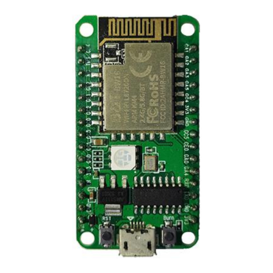
1.Product Overview The BW16-Kit development board is a core development board designed by B&T for the BW16 module, which continues the classic design of the NodeMCU development board, leading all I/O to the pin headers on both sides, on board RGB light, developers can also connect peripherals according to their own needs.Standard pin headers on both sides make operation easier when using bread boards for... -
Page 6: Characteristics
Bluetooth supports high-power mode (7dBm, shares the same PA as Wi-Fi) The Wi-Fi and the BT share the same antenna Application Solution Machine to machine interconnection(M2M) Remote control Main parameters Model BW16-Kit Module package SMD-16 Module size 24*16*3(±0.2)MM Antenna PCB antenna or IPEX Frequency range 2400-2483.5MHz or 5180-5825MHz... -
Page 7: Block Diagram
Block diagram 2.Electrical characteristics Tips: The BW16 module are electrostatic sensitive devices (ESD) and require special ESD precautions typically applied to ESD sensitive components. Proper ESD handling and packaging procedures must be applied throughout the processing, handling, transportation and operation of any application that incorporates the BW18 module. -
Page 8: Rf Performance
深圳市博安通科技股份有限公司 中山市博安通通信技术有限公司 SHENZHEN B&T TECHNOLOGY Co., Ltd ZHONGSHAN B&T TECHNOLOGYCo., Ltd Parameter condition Typical Unit DC3.3V(With an internal pressure regulator and integrate CMOSPA) 1.76 1.8-3.3 Digital I/O power supply voltage DC_IO_33 ( 3.3V I / O rated electric current) 2000 Electrostatic protection(VESD)... -
Page 9: Appearance Dimensions
SHENZHEN B&T TECHNOLOGY Co., Ltd ZHONGSHAN B&T TECHNOLOGYCo., Ltd 3.Appearance dimensions 4.Pin definition The BW16-Kit development board lead out 30 interfaces, refer to below the pin schematic diagram, and the pin function definition table is the interface definition. Page 9 of 14... - Page 10 深圳市博安通科技股份有限公司 中山市博安通通信技术有限公司 SHENZHEN B&T TECHNOLOGY Co., Ltd ZHONGSHAN B&T TECHNOLOGYCo., Ltd Pin function definition table Name Function PA15 SPI1_CS PA27 SWD_DATA Not connect PA26 LP_I2C_SDA/LP_PWM5 PA8/LOG_RX UART_LOG_RXD PA13 LP_PWM1/SPI1_MISO PA14 SPI1_CLK PA30 LP_PWM1 PA12 SPI1_MOSI/LP_PWM0 Ground 3.3V power supply(VDD);recommended greater than 500mA Chip enabling terminal Not connect Ground...
- Page 11 深圳市博安通科技股份有限公司 中山市博安通通信技术有限公司 SHENZHEN B&T TECHNOLOGY Co., Ltd ZHONGSHAN B&T TECHNOLOGYCo., Ltd Ground LP_UART_TXD LP_UART_RXD PA7/LOG_TX UART_LOG_TXD Not connect PA25 LP_I2C_SCL/LP_PWM4 ADC/SWD_CLK Ground 3.3V power supply(VDD);recommended greater than 500mA Not connect Not connect Not connect Not connect Not connect Page 11 of 14...
-
Page 12: Schematic Diagram
深圳市博安通科技股份有限公司 中山市博安通通信技术有限公司 SHENZHEN B&T TECHNOLOGY Co., Ltd ZHONGSHAN B&T TECHNOLOGYCo., Ltd 5.Schematic diagram 6.Design guidance Power supply The development board supports 3.3V or 5V voltage with peak current above 500mA GPIO port Some GPIO ports are lead out from the periphery of the module, if using the proposed resistance of 10-100 ohms in series on the corresponding IO port. -
Page 13: Reflow Welding Curve Diagram
深圳市博安通科技股份有限公司 中山市博安通通信技术有限公司 SHENZHEN B&T TECHNOLOGY Co., Ltd ZHONGSHAN B&T TECHNOLOGYCo., Ltd The IO port of the module is 3.3V, if the master control does not match the IO level of the module, additional level conversion circuit is required If the IO port is directly connected to the peripheral interface, or pin header, it is recommended to reserve the ESD device at the IO line near the IPEX. -
Page 14: Package Information
ZHONGSHAN B&T TECHNOLOGYCo., Ltd Drop speed =2~6 °C / sec, to 183 °C, approximately 15sec Total time = is about 300sec 8. Package information The BW16-Kit development board is packaged for inserted pearl cotton with electrostatic bags. 9. Contact us Official website:https://www.ai-thinker.com http://www.tech-now.com...
Need help?
Do you have a question about the BW16-Kit and is the answer not in the manual?
Questions and answers