
Related Manuals for Opal Kelly XEM6310

Summary of Contents for Opal Kelly XEM6310
- Page 1 (217) 352-9330 | Click HERE Find the Opal Kelly XEM6310-LX45 at our website:...
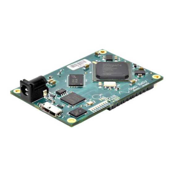
- Page 2 3.0, on-board DDR2 memory, and two 16 MiB Flash memories. The XEM6310 is a compact USB 3.0 (SuperSpeed) FPGA integration module featuring the Xilinx Spar- tan-6 FPGA, 1 Gib (64 Mx16-bit) DDR2 SDRAM, two 128 Mib SPI Flash devices, high-efficiency switch- ing power supplies, and two high-density 0.8-mm expansion connectors.
- Page 3 All rights reserved. Unauthorized duplication, in whole or part, of this document by any means except for brief excerpts in published reviews is prohibited without the express written permission of Opal Kelly Incorporated. Opal Kelly, the Opal Kelly Logo, and FrontPanel are trademarks of Opal Kelly Incorporated.
-
Page 4: Table Of Contents
Applying the XEM6310 ......9 Powering the XEM6310 ......9 Power Budget . - Page 5 BRK6110 Mechanical Drawing ....23 XEM6310 Quick Reference ..... 24 XEM6310 Quick Reference .
-
Page 6: Introducing The Xem6310
FPGA designs with a wide variety of external interface requirements. PCB Footprint A mechanical drawing of the XEM6310 is shown at the end of this manual. The PCB is 75mm x 50mm with four mounting holes (M2 metric screws) spaced as shown in the figure. These mounting holes are electrically isolated from all signals on the XEM6310. -
Page 7: Functional Block Diagram
Samtec Expansion Connector FPGA The XEM6310 is offered in two variants. These two variants are identical except for the FPGA provided. The table below lists some of the differences between the two devices. Please consult the Xilinx documentation for a more thorough comparison. -
Page 8: Dc Power Connector
DC Power Connector The DC power connector on the XEM6310 is part number PJ-102AH from CUI, Inc. It is a stan- dard “canon-style” 2.1mm / 5.5mm jack. The outer ring is connected to DGND. The center pin is connected to +VDC. -
Page 9: Expansion Connectors
PC-based virtual instruments such as LEDs, hex displays, pushbuttons, toggle buttons, and so on. Essentially, this makes your PC a reconfigu- rable I/O board and adds tremendous value to the XEM6310 as an experimentation or prototyp- ing system. -
Page 10: Applying The Xem6310
Applying the XEM6310 Powering the XEM6310 The XEM6310 requires that this supply be clean, filtered, and within the range of 4.5v to 5.5v. This supply must be delivered through the +VDC pins on the two device’s two expansion connec- tors or the DC power connector. -
Page 11: Example Xem6310-Lx150 Fpga Power Consumption
Available: 2,400 mW Supply Heat Dissipation (IMPORTANT!!) Due to the limited area available on the small form-factor of the XEM6310 and the density of logic provided, heat dissipation may be a concern. This depends entirely on the end application and cannot be predicted in advance by Opal Kelly. -
Page 12: Host Interface
XEM6310 User’s Manual Host Interface There are 41 signals that connect the on-board USB microcontroller to the FPGA. These signals comprise the host interface on the FPGA and are used for configuration downloads. After con- figuration, these signals are used to allow FrontPanel communication with the FPGA. -
Page 13: Fpga Flash
DQ3 / HOLD LEDs There are eight LEDs on the XEM6310 in addition to the power LED. Each is wired directly to the FPGA according to the pin mapping tables at the end of this document. The LED anodes are connected to a pull-up resistor to +3.3VDD and the cathodes wired directly to the FPGA on Bank 2 with a bank I/O voltage of 1.8v. -
Page 14: Clock Configuration (Source Synchronous)
Spartan-6 has integrated memory control blocks to communicate with the external DDR2 mem- ory on the XEM6310. This is instantiated using the Xilinx Core Generator (memory interface generator, or MIG) to create a suitable memory controller for your design. You should read and become familiar with the DDR2 SDRAM datasheet as well as MIG and the core datasheet. -
Page 15: Jtag
The JTAG connections on the FPGA are wired directly to the expansion connector JP2 on the XEM6310 to facilitate FPGA configuration and ChipScope usage using a Xilinx JTAG cable. The BRK6110 has these signals connected to a 2-mm header compatible with the Xilinx JTAG cable. -
Page 16: Non-Volatile Encryption Key Storage (Efuse)
Fuse Expansion Connectors Opal Kelly Pins is an interactive online reference for the expansion connectors on all Opal Kelly FPGA integration modules. It provides additional information on pin capabilities, pin character- istics, and PCB routing. Additionally, Pins provides a tool for generating constraint files for place and route tools. -
Page 17: Jp2
The Spartan-6 FPGA allows users to set I/O bank voltages in order to support several different I/O signalling standards. This functionality is supported by the XEM6310 by allowing the user to connect independent supplies to the FPGA VCCO pins on two of the FPGA banks. -
Page 18: Brk6110 Breakout Board
XEM6310. It provides standard 2-mm thru-hole connections to the 0.8-mm high-density connectors on the XEM6310 and a DC power connector (2.1mm/5.5mm, center positive) for pro- viding +VDC to the XEM6310. Please visit the Pins reference for the XEM6310 for pin mapping details. -
Page 19: Pin Lists
XEM6310 User’s Manual Pin Lists As the primary reference for Opal Kelly integration module expansion connectors, Pin Lists con- tain a comprehensive table of the FPGA-to-Connector data including connector pin, FPGA pin, signal description, routed length (when applicable), breakout board pin mapping, FPGA I/O bank, and other properties. -
Page 20: Peripherals
XEM6310 User’s Manual The constraints files include additional mapping information for other peripherals on the module such as memory, clock oscillators, and LEDs. Peripherals A Pins Peripheral is a project definition where you can enter your top-level HDL design nets to have Pins generate a complete constraint file for you. -
Page 21: Migrating Hardware From The Xem6010 To The Xem6310
XEM6310 User’s Manual Migrating Hardware from the XEM6010 to the XEM6310 The XEM6310 was designed to be as compatible as possible with our XEM6010 in order to facili- tate customer design migration with minimal changes. The physical dimentions and connector footprints are identical. -
Page 22: Pcb Version History
XEM6310 User’s Manual PCB Version History 20120517 First production PCB. www.opalkelly.com... -
Page 23: Xem6310 Mechanical Drawing
XEM6310 User’s Manual XEM6310 Mechanical Drawing 50.00 47.00 42.33 40.50 31.50 24.08 17.66 11.23 3.00 2.33 50.00 45.00 5.00 12.78 8.28 4.57 1.75 1.55 All dimensions in mm www.opalkelly.com... -
Page 24: Brk6110 Mechanical Drawing
XEM6310 User’s Manual BRK6110 Mechanical Drawing All dimensions in mm. 120.00 117.00 112.71 111.00 108.56 106.41 98.00 92.73 73.00 65.00 58.26 29.00 27.00 3.00 www.opalkelly.com... -
Page 25: Xem6310 Quick Reference
XEM6310 User’s Manual XEM6310 Quick Reference Length Length FPGA Pin Connection FPGA Pin (mm) Connection FPGA Pin (mm) DGND +3.3VDD VBATT +3.3VDD batt JTAG_TCK +3.3VDD AB14 JTAG_TMS JTAG_TDO AB19 JTAG_TDI VREF_1 Bank 1 VREF AB17 L22N_2 27.043 RFUSE Fuse AB16... -
Page 26: Xem6310 Quick Reference
XEM6310 User’s Manual XEM6310 Quick Reference Length Length Connection FPGA Pin (mm) Connection FPGA Pin (mm) +VDC DGND +VDC +1.2VDD +VDC +1.2VDD +1.8VDD L23P_2 51.413 +3.3VDD L43P_2 40.650 +3.3VDD L43N_2 49.296 +3.3VDD DGND L60P_1 56.675 L74P_1 48.345 L60N_1 56.761 L74N_1 48.805...
Need help?
Do you have a question about the XEM6310 and is the answer not in the manual?
Questions and answers