Sony CMT-SP55TC Service Manual
Hide thumbs
Also See for CMT-SP55TC:
- Operating instructions manual (44 pages) ,
- Service manual (58 pages)
Table of Contents
Advertisement
Quick Links
SERVICE MANUAL
Ver.1.1 2001.03
CMT-SP55TC
PARTS LIST(ACCESSORIES & PACKING MATERIALS)
Part No.
1-476-136-11 REMOTE COMMANDER (RM-SSP55)
1-501-374-11 ANTENNA, LOOP (AM)
1-501-804-11 ANTENNA (FM)(EXCEPT MY, SP)
1-501-659-41 ANTENNA (FM) (MY, SP)
1-792-924-11 CORD (WITH CONNECTOR)(20P)(30cm)
1-792-954-11 CORD, CONNECTION (19P)(40cm)
4-230-235-11 MANUAL, INSTRUCTION (ENGLISH)(AEP, UK, MY, SP)
4-230-235-21 MANUAL, INSTRUCTION (FRENCH, SPANISH)(AEP, MY, SP)
4-230-235-31 MANUAL, INSTRUCTION (GERMAN, DUTCH)(AEP)
4-230-235-41 MANUAL, INSTRUCTION (ITALIAN, PORTUGUESE)(AEP)
4-230-235-51 MANUAL, INSTRUCTION (DANISH, FINNISH, SWEDISH)(AED)
4-230-235-61 MANUAL, INSTRUCTION (CHINESE)(MY, SP)
4-230-235-71 MANUAL, INSTRUCTION (KOREAN)(KR)
4-981-643-21 COVER, BATTERY (FOR RM-SSP55)
•Abbreviation
AED : North European
MY : Malaysia
SP
KR : Korea
Sony Corporation
9-929-541-12
Audio Entertainment Group
2001C0900-1
© 2001. 3
General Engineering Dept.
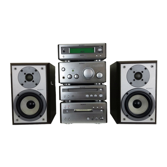
CMT-SP55TC
• CMT-SP55TC is composed of following models.
As for the service manual, it is issued for each
component model, then, please refer to it.
COMPONENT MODEL NAME FOR CMT-SP55TC
AMPLIFIER CD PLAYER TAPE DECK
TA-SP55
CDP-SP55
Description
: Singapore
TUNER
TC-SP55
ST-SP55
MICRO HI-FI COMPONENT SYSTEM
AEP Model
UK Model
E Model
SPEAKER SYSTEM
SS-CSP55
Advertisement
Chapters
Table of Contents

Related Manuals for Sony CMT-SP55TC


Summary of Contents for Sony CMT-SP55TC
- Page 1 AEP Model UK Model Ver.1.1 2001.03 E Model • CMT-SP55TC is composed of following models. As for the service manual, it is issued for each component model, then, please refer to it. COMPONENT MODEL NAME FOR CMT-SP55TC AMPLIFIER CD PLAYER TAPE DECK...
- Page 2 CDP-SP55 SERVICE MANUAL AEP Model UK Model E Model CDP-SP55 is the CD section in CMT-SP55MD or CMT-SP55TC. Model Name Using Similar Mechanism CD Mechanism Type CDM55C-K6BD38 Base Unit Type BU-K6BD38 Optical Pick-up Type KSM-213DCP/Z-NP SPECIFICATIONS General System Compact disc and digital audio system Approx.
-
Page 3: Table Of Contents
TABLE OF CONTENTS 1. SERVICING NOTE ·························································· 4 2. GENERAL ·········································································· 6 3. DISASSEMBLY 3-1. Case ···················································································· 7 3-2. Front Panel Assy ································································· 7 3-3. CD Mechanism Deck (CDM55C-K6BD38) ······················ 8 3-4. Main Board ········································································· 8 3-5. CAM, GEAR ······································································ 9 3-6. - Page 4 COMPONENTS IDENTIFIED BY MARK 0 OR DOTTED LINE WITH MARK 0 ON THE SCHEMATIC DIAGRAMS AND IN THE PARTS LIST ARE CRITICAL TO SAFE OPERATION. REPLACE THESE COMPONENTS WITH SONY PARTS WHOSE PART NUMBERS APPEAR AS SHOWN IN THIS MANUAL OR IN SUPPLEMENTS PUBLISHED BY SONY.
-
Page 5: Servicing Note
SECTION 1 SERVICING NOTE This unit cannot be repaired by itself. When repairing, connect the whole system except for the speaker. CD Text Display • This unit displays CD text. Text is displayed for the first 50 track only and will not be displayed from the 51st track onwards. Do not suspect a fault in this case. In some cases, some special characters will not be displayed and may be replaced by other characters. - Page 6 Aging Mode • Mode for repeating operations of the CD player and TC deck automatically. When errors occur: Aging stops and a message indicating that an error has occurred such as “CD MEC ERR” is displayed. (For details of errors, refer to “Error History Display Mode”.) When no errors occur: Aging is repeatedly performed.
-
Page 7: General
SECTION 2 This section is extracted from instruction manual. GENERAL PLAY MODE button lm button REPEAT button ML button H button A button S button S indicator s button H indicator... -
Page 8: Disassembly
SECTION 3 DISASSEMBLY Case Front Panel Assy Main Board (Page 8) CD Mechanism Deck (CDM55C-K6BD38) Cam, Gear (Page 8) (Page 9) Holder Assy Optical pick-up BD Board (Page 9) (Page 10) (Page 10) 3-1. CASE 4 case 1 two screws (case 3 TP2) 1 two screws (case 3 TP2) -
Page 9: Main Board
3-3. CD MECHANISM DECK (CDM55C-K6BD38) 5 CD mechanism deck 3 screw (BVTP 3x8) two claws 2 connector (CN112) 1 flat type wire (19 core) (CN713) 3-4. MAIN BOARD 2 main board 1 screw (BVTP 3x8) -
Page 10: Cam, Gear
3-5. CAM, GEAR 4 belt (CDM55) 5 bushing 6 pulley (LDG) 8 gear (B) 9 gear (A) 7 roller 0 cam (CDM55) 2 Push the claw in tne direction of arrow C. 1 Pull out the tray in the arrow direction A, and release the lock while pressing this claw in the arrow direction B. -
Page 11: Optical Pick-Up
3-7. OPTICAL PICK-UP 3 Optical pick-up 1 Release the lever in the 4 flat type wire arrow direction B. (16 core) 2 sled shaft 3-8. BD BOARD 2 Remove the four solders. M101 IC102 M102 IC103 IC101 3 BD board 1 screw (BVTP 2.6x8) -
Page 12: Electrical Adjustment
SECTION 4 ELECTRICAL ADJUSTMENT Note : Note: Clear RF signal waveform means that the shape “◊” can be 1. CD Block is basically designed to operate without adjustment. clearly distinguished at the center of the waveform. Therefore, check each item in order given. 2. - Page 13 Adjustment Location: [BD BOARD] (Conductor Side) (XPCK) (AGCCON) IC103 (TEO) IC101 (FEO) (FEI) (VC) (RF) (DGND)
-
Page 14: Diagrams
SECTIOIN 5 DIAGRAMS THIS NOTE IS COMMON FOR PRINTED WIRING • Indication of transistor BOARDS AND SCHEMATIC DIAGRAMS. (In addition to this, the necessary note is printed in each block.) These are omitted. For schematic diagrams. Note: • All capacitors are in µF unless otherwise noted. pF: µµF 50 WV or less are not indicated except for electrolytics and tantalums. -
Page 15: Circuit Boards Location
• WAVEFORMS – BD BOARD – IC101 yj (XTAO) IC101 ra (TE) PLAY MODE PLAY MODE approx 300mVp-p 6.4Vp-p 59nsec IC101 ta (RFAC) IC101 el (FE) PLAY MODE PLAY MODE approx 400mVp-p 1.2Vp-p 1µsec/div 5-1. CIRCUIT BOARDS LOCATION BD board LOADING board MAIN board PANEL 2 board... -
Page 16: Block Diagram
CDP-SP55 5-2. BLOCK DIAGRAM IC701 DIGITAL OPTICAL PICK-UP BLOCK (KSM-213DCP/Z-NP) IC101 OPTICAL DIGITAL SERVO DETECTOR IC103 DIGITAL SIGNAL PRCESSOR RF AMP DIGITAL D OUT DOUT ERROR CORRECTOR CN701 S771-778 RF AC RF EQ CD KEY SUMMING MATRIX OVER SAMPLING DEMODULATOR SERIAL IN DIGITAL Q741... -
Page 17: Printed Wiring Board - Bd Section
CDP-SP55 5-3. PRINTED WIRING BOARD – BD SECTION – • See page 14 for Circuit Boards Location. There are a few cases that the part isn't mounted in model is printed on diagram. -
Page 18: Schematic Diagram - Bd Section
CDP-SP55 5-4. SCHEMATIC DIAGRAM – BD SECTION – • See page 14 for Waveforms. • See page 20 for IC Block Diagrams. - Page 19 CDP-SP55 5-5. PRINTED WIRING BOARD – MAIN SECTION – • See page 14 for Circuit Boards Location. • Semiconductor Location Ref. No. Location D711 D712 D713 D714 D731 D741 IC701 IC721 IC731 IC741 Q741 Q742 There are a few cases that the part isn't mounted in model is printed on diagram.
-
Page 20: Schematic Diagram - Main Section
CDP-SP55 5-6. SCHEMATIC DIAGRAM – MAIN SECTION – • See page 21 for IC Block Diagrams. -
Page 21: Printed Wiring Board - Loading Section
CDP-SP55 5-9. IC BLOCK DIAGRAM 5-7. PRINTED WIRING BOARD – LOADING SECTION – IC101 CXD2587Q (BD BOARD) (Page 18) ERROR ASYMMETRY DIGITAL DIGITAL CORRECTOR CORRECTION LRCK OPERATIONAL AMPLIFIER PCMD INTERFACE DEMODULATOR ANALOG SWITCH CONVERTER EMPH XVDD CLOCK XTSL GENERATOR (OPEN/CLOSE SW) XTAI TIMING TES1... - Page 22 IC103 CXA2568M-T6 (BD BOARD) APC PD AMP LC/PD LD_ON HOLD AGCVTH VREF APC LD AMP HOLD_SW AGCCONT (50%/30% OFF) RF_BOT RFTC RF SUMMING AMP RF_EQ_AMP RF_1 ERROR AMP FOCUS TRACKING ERROR AMP VC BUFFER IC731 LB1641 (MAIN BOARD) T.S.D O.C.P MOTOR MOTOR DRIVE...
-
Page 23: Exploded Views
SECTION 6 EXPLODED VIEWS NOTE: • -XX, -X mean standardized parts, so they may • Hardware (# mark) list and accessories and The components identified by mark 0 or have some differences from the original one. packing materials are given in the last of this dotted line with mark 0 are critical for safety. -
Page 24: Cd Mechanism Deck Section (Cdm55C-K6Bd38)
6-2. CD MECHANISM DECK SECTION (CDM55C-K6BD38) not supplied M103 BU-K6BD38 not supplied Ref. No. Part No. Description Remarks Ref. No. Part No. Description Remarks 1-674-336-21 LOADING BOARD 4-220-238-01 GEAR (B) 4-224-894-11 TRAY (CDM55D) 1-452-925-21 MAGNET ASSY 4-220-229-01 LEVER (SW) X-4953-195-1 PULLEY (AT) ASSY 4-220-239-11 SPRING, TORSION 4-985-672-01 SCREW (+PTPWHM2.6), FLOATING 4-227-679-01 INSULATOR (213) -
Page 25: Base Unit Section (Bu-6Bd38)
6-3. BASE UNIT SECTION (BU-K6BD38) The components identified by mark 0 or dotted line with mark 0 are critical for safety. Replace only with part number specified. Ref. No. Part No. Description Remarks A-4724-934-A BD BOARD, COMPLETE 0 552 8-820-116-01 OPTICAL PICK-UP KSM-213DCP/Z-NP 1-792-024-11 WIRE (FLAT TYPE) (16 CORE) 4-951-620-01 SCREW (2.6X8), +BVTP... -
Page 26: Electrical Parts List
SECTION 7 ELECTRICAL PARTS LIST NOTE: • Due to standardization, replacements in the • COILS Ref. No. Part No. Description Remarks Ref. No. Part No. Description Remarks When indicating parts by reference number, parts list may be different from the parts uH: µH please include the board name. - Page 27 LOADING MAIN PANEL 1 Ref. No. Part No. Description Remarks Ref. No. Part No. Description Remarks R147 1-216-069-00 METAL CHIP 6.8K 1/10W < CONNECTOR > R148 1-216-001-00 METAL CHIP 1/10W R149 1-216-001-00 METAL CHIP 1/10W * CN112 1-568-954-11 PIN, CONNECTOR 5P CN701 1-794-498-11 SOCKET, CONNECTOR 20P R158...
- Page 28 PANEL 1 PANEL 2 Ref. No. Part No. Description Remarks Ref. No. Part No. Description Remarks < SWITCH > S771 1-771-410-21 SWITCH, TACTILE (lm) S772 1-771-410-21 SWITCH, TACTILE (ML) S773 1-771-410-21 SWITCH, TACTILE (A) S774 1-771-410-21 SWITCH, TACTILE (s) S775 1-771-410-21 SWITCH, TACTILE (S) S776 1-771-410-21 SWITCH, TACTILE (H)
- Page 29 SERVICE MANUAL AEP Model UK Model Ver 1.1 2001.03 E Model TC-SP55 is the deck section in CMT-SP55TC, and TC-SP55 is sold in the option as a tape deck of CMT-SP55MD. Model Name Using Similar Mechanism Tape Transport Mechanism Type...
- Page 30 COMPONENTS IDENTIFIED BY MARK 0 OR DOTTED LINE WITH MARK 0 ON THE SCHEMATIC DIAGRAMS AND IN THE PARTS LIST ARE CRITICAL TO SAFE OPERATION. REPLACE THESE COMPONENTS WITH SONY PARTS WHOSE PART NUMBERS APPEAR AS SHOWN IN THIS MANUAL OR IN SUPPLEMENTS PUBLISHED BY SONY.
-
Page 31: Servicing Note
SECTION 1 SERVICING NOTE This unit cannot be repaired by itself. When repairing, connect the whole system except for the speaker. Cold Reset • When the AC cord is removed, COLD RESET is done with TC-SP55. ST Test Mode Procedure : 1. - Page 32 Aging Mode • Mode for repeating operations of the CD player and TC deck automatically. When errors occur: Aging stops and a message indicating that an error has occurred such as “CD MEC ERR” is displayed. (For details of errors, refer to “Error History Display Mode”.) When no errors occur: Aging is repeatedly performed.
-
Page 33: General
SECTION 2 GENERAL CD SYNC REC button M L button CD SYNC REC indicator l m button z REC button s button z REC indicator S button h indicator H button H indicator h button S indicator DIRECTION button A button DOLBY NR button... -
Page 34: Disassembly
SECTION 3 DISASSEMBLY Case Front Panel Assy Mechanism Assy (Page 7) Main Board (Page 7) Pinch Roller BLK Assy, Belt (Page 8) Note: Follow the disassembly procedure in the numerical order given. 4 case 3-1. CASE 1 two screws (case 3 TP2) 1 two screws (case 3 TP2) 3-2. -
Page 35: Mechanism Assy
3-3. MECHANISM ASSY 3 mechanism assy 2 two screws 2 two screws (BVTP 3x10) (BVTP 3x10) 1 connector (CN101) 1 connector (CN601) 1 connector (CN602) 3-4. MAIN BOARD 4 three screws (BVTP 3x8) 5 main board 1 three screws (BVTP 3x8) 2 claw 2 claw... -
Page 36: Pinch Roller Blk Assy, Belt
3-5. PINCH ROLLER BLK ASSY, BELT 6 pinch roller BLK L assy belt main 4 pinch roller BLK R assy 2 mechanism deck 5 claw 3 claw 1 two screws 7 belt main 1 two screws F/R belt 8 F/R belt... -
Page 37: Test Mode
SECTION 4 TEST MODE 4-1. TEST MODE FOR NOT CONNECTING THE WHOLE SYSTEM (When connecting TA-SP55,ST-SP55,TC-SP55) 4-1-1. SETTING THE TEST MODE Procedure: 1. When the power ON, press the ?/1 button (TA) while pressing the s button (TC) and CD SYNC REC buttons (TC) together. 2. - Page 38 4-2. TEST MODE FOR CONNECTING THE WHOLE SYSTEM 4-2-1. TC Aging Mode (Connecting The Whole System) • Mode for repeating operations of the CD player and TC deck automatically. When errors occur: Aging stops and a message indicating that an error has occurred such as “CD MEC ERR” is displayed. (For details of errors, refer to “Error History Display Mode”.) When no errors occur: Aging is repeatedly performed.
-
Page 39: Mechanical Adjustments
SECTION 5 SECTION 6 MECHANICAL ADJUSTMENTS ELECTRICAL ADJUSTMENTS Precaution 0 DB=0.775V 1. Clean the following parts with a denatured alcohol-moistened swab: Note: Before starting the adjustment, measure performance of the record/playback heads pinch rollers machine. Perform adjustment only when the measured erase head rubber belts performances do not satisfy the specifications. - Page 40 3. Phase check Playback Level Adjustment Model: FWD playback Procedure: test tape Mode: FWD playback P-4-A100 oscilloscope (10kHz, –10dB) test tape 47kW L-CH P-4-L300 (315Hz, 0dB) level meter R-CH 47kW AUX OUT AUX OUT (on ST-SP55) (on ST-SP55) 4. Perform steps 1 to 3 in the FWD playback mode. Adjust RV211 (L-CH) and RV261 (R-CH), so that adjustment within 5.
- Page 41 Record Level Adjustment Procedure: 1. Record mode. AUX IN (on ST-SP55) 315Hz 50 mV (–23.8 dB) AF OSC blank tape 600 Ω CS-123 attenuator 2. Playback mode. recorded level meter position AUX OUT (on ST-SP55) 3. Confirm playback the signal recorded in step 1 become adjust- ment level as follows.
-
Page 42: Diagrams
SECTION 7 DIAGRAMS THIS NOTE IS COMMON FOR PRINTED WIRING • Indication of transistor BOARDS AND SCHEMATIC DIAGRAMS. (In addition to this, the necessary note is printed in each block.) These are omitted. For schematic diagrams. Note: • All capacitors are in µF unless otherwise noted. pF: µµF 50 WV or less are not indicated except for electrolytics and tantalums. -
Page 43: Block Diagram
TC-SP55 7-1. BLOCK DIAGRAM IC401 DDOLBY NR 28 27 PB-A/B CN701 PB OUT TC-L LM ON/ TC.M R-CH TC-R TAPE MECHANISM ASSY DOLBY NR CMAL2Z720A NORM/ HIGH RV211 DOLBY NR ON/ IC201 PLAYBACK REC.PB.P RV401 LEVEL REC LEVEL REC OUT DOLBY TYPE B REC-L... -
Page 44: Schematic Diagram - Main Section
TC-SP55 7-2. SCHEMATIC DIAGRAM – MAIN SECTION – • See page 14 for Waveforms. • See page 19 for IC Pin Functions. • See page 20 for IC Block Diagrams. FUNCTION... - Page 45 TC-SP55 7-3. PRINTED WIRING BOARD – MAIN SECTION – • Semiconductor Location Ref. No. Location D601 D602 D603 D604 D611 D621 D622 D623 D624 D701 IC101 IC201 IC401 IC601 IC602 IC603 IC604 IC605 IC701 IC702 Q501 Q502 Q503 Q601 Q602 Q603 Q604 Q701...
-
Page 46: Schematic Diagram - Panel Section
TC-SP55 7-4. SCHEMATIC DIAGRAM – PANEL SECTION – 7-5. PRINTED WIRING BOARD – PANEL SECTION – • Semiconductor Location Ref. No. Location D911 D912 D913 D914 D915 There are a few cases that the part isn’t mounted in model is printed on diagram. -
Page 47: Ic Pin Functions
7-6. IC PIN FUNCTIONS • IC701 M38513M4-C59FP SYSTEM CONTROL (MAIN BOARD) Pin No. Pin Name Function — Power supply.(+5V) VREF — Analog Reference Voltage. AVSS — Ground. — Not used. — Not used. P.DOWN POWER DOWN signal control signal input. H: Normal L: STANDBY mode DOLBY DOLBY B NR control signal output. -
Page 48: Ic Block Diagrams
7-7. IC BLOCK DIAGRAMS IC101 µPC1330HA (MAIN BOARD) INVERTER COMPARATER SW R1 SW P1 CONT SW P2 SW R2 IC601 LB1641 (MAIN BOARD) T.S.D O.C.P MOTOR MOTOR DRIVE DRIVE FWD/REV/STOP CONTROL LOGIC... -
Page 49: Exploded View
Ver 1.1 2001.03 SECTION 8 EXPLODED VIEW NOTE: • Hardware (# mark) list is given in the last of • -XX and -X mean standardized parts, so they The components identified by mark 0 or dotted line with mark may have some difference from the original the electrical parts list. -
Page 50: Electrical Parts List
SECTION 9 MAIN ELECTRICAL PARTS LIST NOTE: • Due to standardization, replacements in the • Items marked “*” are not stocked since they The components identified by mark 0 or dotted line with mark parts list may be different from the parts speci- are seldom required for routine service. - Page 51 MAIN Ref. No. Part No. Description Remark Ref. No. Part No. Description Remark D603 8-719-911-19 DIODE 1SS133T-72 R312 1-249-433-11 CARBON 1/4W D604 8-719-210-21 DIODE 11EQS04-NTA2B R361 1-249-430-11 CARBON 1/4W D611 8-719-947-16 DIODE MTZJ-T-72-5.1A R362 1-249-433-11 CARBON 1/4W D621 8-719-024-99 DIODE 11ES2-NTA2B R401 1-249-435-11 CARBON 1/4W...
- Page 52 MAIN PANEL Ref. No. Ref. No. Part No. Part No. Description Description Remark Remark Ref. No. Ref. No. Part No. Part No. Description Description Remark Remark < VARIABLE RESISTOR > ACCESSORIES & PACKING MATERIALS ******************************** RV211 1-241-762-11 RES, ADJ, CARBON 2.2K RV261 1-241-762-11 RES, ADJ, CARBON 2.2K 1-792-923-11 CORD (WITH CONNECTOR) (AEP,UK,AED)
- Page 53 SS-CSP55 SERVICE MANUAL AEP Model UK Model E Model This set is the speaker system in CMT-SP55MD/SP55TC. SPECIFICATIONS Speaker system : 2-way, bass-reflex type Speaker units Woofer: 12 cm dia., glass-fiber cone type Tweeter: 2.5 cm dia., soft dome type Nominal impedance 8 ohms Dimensions (w/h/d) incl.
- Page 54 4-874-614-51 SCREW (4) (3.5X20), TAPPING 1-757-422-11 CORD SPEAKER (1.5 m) 4-228-872-01 RING. ORNAMENTAL SP101 1-529-748-11 SPEAKER (12 cm) SP201 1-529-749-11 SPEAKER (2.5 cm) ************************************************************** Sony Corporation 9-929-534-11 2000H091661-1 Audio Entertainment Group Printed in Japan © 2000. 08 Published by HA Quality Assurance Dept.
- Page 55 ST-SP55 SERVICE MANUAL AEP Model UK Model E Model ST-SP55 is the tuner section in CMT-SP55MD or CMT-SP55TC. SPECIFICATIONS General FM stereo, FM/AM superheterodyne tuner Input Dimensions (w/h/d) incl. projecting parts and controls AUX IN (phono jacks): voltage 250 mV, impedance Approx.
- Page 56 COMPONENTS IDENTIFIED BY MARK 0 OR DOTTED LINE WITH MARK 0 ON THE SCHEMATIC DIAGRAMS AND IN THE PARTS LIST ARE CRITICAL TO SAFE OPERATION. REPLACE THESE COMPONENTS WITH SONY PARTS WHOSE PART NUMBERS APPEAR AS SHOWN IN THIS MANUAL OR IN SUPPLEMENTS PUBLISHED BY SONY.
-
Page 57: Service Note
SECTION 1 SERVICE NOTE This unit cannot be repaired by itself. When repairing, connect the whole system except for the speaker. CD Text Display • This unit displays CD text. Text is displayed for the first 50 track only and will not be displayed from the 51st track onwards. Do not suspect a fault in this case. In some cases, some special characters will not be displayed and may be replaced by other characters. -
Page 58: Diagrams
SECTION 3 DIAGRAMS • WAVEFORMS THIS NOTE IS COMMON FOR PRINTED WIRING BOARDS AND SCHEMATIC DIAGRAMS. – MAIN BOARD – (In addition to this, the necessary note is printed in each block.) IC701 qa XCOUT For schematic diagrams. Note: 2.7Vp-p •... -
Page 59: Block Diagram
ST-SP55 3-2. BLOCK DIAGRAM J210(2/2) AUX OUT IC401 INPUT SELECT/EVR Q221 R-CH IC231 MUTE LSELO BUFFER CN201 LOUT ST-L MD-L ST MUTE R-CH CD-L FM 75Ω RDS INT SEL-L TUNER RDS DATA UNIT STEREO S923 Q201 TUNED TUNING ST CE MODE CONTROL ST DOUT... -
Page 60: Schematic Diagram - Main Section
ST-SP55 3-3. SCHEMATIC DIAGRAM – MAIN SECTION – (Page 8) PIN FUNCTION (Page 8) (Page 8) - Page 61 ST-SP55 3-4. PRINTED WIRING BOARD – MAIN SECTION – (Page 9) • Semiconductor Location Ref. No. Location D201 D282 D283 D291 D301 D701 D702 D731 D733 IC202 IC231 IC281 IC282 IC283 IC401 IC701 IC702 Q201 Q221 Q271 Q281 Q282 Q291 Q301 Q701 Q702...
-
Page 62: Schematic Diagram - Panel Section
ST-SP55 3-5. SCHEMATIC DIAGRAM – PANEL SECTION – LCD BACK LIGHT (Page 6) (Page 6) (Page 6) -
Page 63: Printed Wiring Board - Panel Section
ST-SP55 3-6. PRINTED WIRING BOARD – PANEL SECTION – (Page 7) (Page 7) (Page 7) There are a few cases that the part isn't mounted in model is printed on diagram. -
Page 64: Ic Pin Functions
ST-SP55 3-7. IC PIN FUNCTIONS • IC701 M30620MCA-A67FP MASTER CONTROL (MAIN BOARD) Pin No. Pin Name Function Pin No. Pin Name Function DP_DATA LCD data output. — Ground. DP_CLK LCD clock output. — Not used. DP_CS LCD chip STB signal output. —... -
Page 65: Ic Block Diagram
3-8. IC BLOCK DIAGRAM IC401 LC75342 LOUT RROUT LBASS2 RBASS2 LBASS1 RBASS1 LTRE RTRE LSELO RSELO... -
Page 66: Exploded View
SECTION 4 EXPLODED VIEW NOTE: • Abbreviation • Items marked “*” are not stocked since they are The components identified by AED : North European model seldom required for routine service. Some delay mark 0 or dotted line with mark should be anticipated when ordering these items. -
Page 67: Electrical Parts List
SECTION 5 MAIN ELECTRICAL PARTS LIST Ref. No. Part No. Description Remarks Ref. No. Part No. Description Remarks Note: • SEMICONDUCTORS • Due to standardization, replacements in the parts The components identified by In each case, u: µ , for example: list may be different from the parts specified in the mark 0 or dotted line with mark uA...: µ... - Page 68 MAIN Ref. No. Part No. Description Remarks Ref. No. Part No. Description Remarks C732 1-126-925-11 ELECT 470uF R213 1-249-418-11 CARBON 1.2K 1/4W F C733 1-104-664-11 ELECT 47uF R214 1-249-429-11 CARBON 1/4W C734 1-104-664-11 ELECT 47uF C735 1-164-159-11 CERAMIC 0.1uF R215 1-249-421-11 CARBON 2.2K 1/4W F...
- Page 69 PIN JACK MAIN PANEL Ref. No. Part No. Description Remarks Ref. No. Part No. Description Remarks R717 1-249-429-11 CARBON 1/4W < CONNECTOR > R718 1-249-429-11 CARBON 1/4W R719 1-247-807-31 CARBON 1/4W CN901 1-784-731-11 CONNECTOR, FFC 9P R720 1-249-429-11 CARBON 1/4W CN902 1-580-471-11 SOCKET, CONNECTOR 6P R721...
- Page 70 ST-SP55 Ref. No. Part No. Description Remarks Ref. No. Part No. Description Remarks Sony Corporation 9-929-536-11 2000I097551-1 Audio Entertainment Group Printed in Hungary ©2000.9 Published by General Engineering Dept.
- Page 71 SERVICE MANUAL AEP Model UK Model Ver 1.1 2001.03 E Model TC-SP55 is the deck section in CMT-SP55TC, and TC-SP55 is sold in the option as a tape deck of CMT-SP55MD. Model Name Using Similar Mechanism Tape Transport Mechanism Type...
- Page 72 COMPONENTS IDENTIFIED BY MARK 0 OR DOTTED LINE WITH MARK 0 ON THE SCHEMATIC DIAGRAMS AND IN THE PARTS LIST ARE CRITICAL TO SAFE OPERATION. REPLACE THESE COMPONENTS WITH SONY PARTS WHOSE PART NUMBERS APPEAR AS SHOWN IN THIS MANUAL OR IN SUPPLEMENTS PUBLISHED BY SONY.
-
Page 73: Servicing Note
SECTION 1 SERVICING NOTE This unit cannot be repaired by itself. When repairing, connect the whole system except for the speaker. Cold Reset • When the AC cord is removed, COLD RESET is done with TC-SP55. ST Test Mode Procedure : 1. - Page 74 Aging Mode • Mode for repeating operations of the CD player and TC deck automatically. When errors occur: Aging stops and a message indicating that an error has occurred such as “CD MEC ERR” is displayed. (For details of errors, refer to “Error History Display Mode”.) When no errors occur: Aging is repeatedly performed.
-
Page 75: General
SECTION 2 GENERAL CD SYNC REC button M L button CD SYNC REC indicator l m button z REC button s button z REC indicator S button h indicator H button H indicator h button S indicator DIRECTION button A button DOLBY NR button... -
Page 76: Disassembly
SECTION 3 DISASSEMBLY Case Front Panel Assy Mechanism Assy (Page 7) Main Board (Page 7) Pinch Roller BLK Assy, Belt (Page 8) Note: Follow the disassembly procedure in the numerical order given. 4 case 3-1. CASE 1 two screws (case 3 TP2) 1 two screws (case 3 TP2) 3-2. -
Page 77: Mechanism Assy
3-3. MECHANISM ASSY 3 mechanism assy 2 two screws 2 two screws (BVTP 3x10) (BVTP 3x10) 1 connector (CN101) 1 connector (CN601) 1 connector (CN602) 3-4. MAIN BOARD 4 three screws (BVTP 3x8) 5 main board 1 three screws (BVTP 3x8) 2 claw 2 claw... -
Page 78: Pinch Roller Blk Assy, Belt
3-5. PINCH ROLLER BLK ASSY, BELT 6 pinch roller BLK L assy belt main 4 pinch roller BLK R assy 2 mechanism deck 5 claw 3 claw 1 two screws 7 belt main 1 two screws F/R belt 8 F/R belt... -
Page 79: Test Mode
SECTION 4 TEST MODE 4-1. TEST MODE FOR NOT CONNECTING THE WHOLE SYSTEM (When connecting TA-SP55,ST-SP55,TC-SP55) 4-1-1. SETTING THE TEST MODE Procedure: 1. When the power ON, press the ?/1 button (TA) while pressing the s button (TC) and CD SYNC REC buttons (TC) together. 2. - Page 80 4-2. TEST MODE FOR CONNECTING THE WHOLE SYSTEM 4-2-1. TC Aging Mode (Connecting The Whole System) • Mode for repeating operations of the CD player and TC deck automatically. When errors occur: Aging stops and a message indicating that an error has occurred such as “CD MEC ERR” is displayed. (For details of errors, refer to “Error History Display Mode”.) When no errors occur: Aging is repeatedly performed.
-
Page 81: Mechanical Adjustments
SECTION 5 SECTION 6 MECHANICAL ADJUSTMENTS ELECTRICAL ADJUSTMENTS Precaution 0 DB=0.775V 1. Clean the following parts with a denatured alcohol-moistened swab: Note: Before starting the adjustment, measure performance of the record/playback heads pinch rollers machine. Perform adjustment only when the measured erase head rubber belts performances do not satisfy the specifications. - Page 82 3. Phase check Playback Level Adjustment Model: FWD playback Procedure: test tape Mode: FWD playback P-4-A100 oscilloscope (10kHz, –10dB) test tape 47kW L-CH P-4-L300 (315Hz, 0dB) level meter R-CH 47kW AUX OUT AUX OUT (on ST-SP55) (on ST-SP55) 4. Perform steps 1 to 3 in the FWD playback mode. Adjust RV211 (L-CH) and RV261 (R-CH), so that adjustment within 5.
- Page 83 Record Level Adjustment Procedure: 1. Record mode. AUX IN (on ST-SP55) 315Hz 50 mV (–23.8 dB) AF OSC blank tape 600 Ω CS-123 attenuator 2. Playback mode. recorded level meter position AUX OUT (on ST-SP55) 3. Confirm playback the signal recorded in step 1 become adjust- ment level as follows.
-
Page 84: Diagrams
SECTION 7 DIAGRAMS THIS NOTE IS COMMON FOR PRINTED WIRING • Indication of transistor BOARDS AND SCHEMATIC DIAGRAMS. (In addition to this, the necessary note is printed in each block.) These are omitted. For schematic diagrams. Note: • All capacitors are in µF unless otherwise noted. pF: µµF 50 WV or less are not indicated except for electrolytics and tantalums. -
Page 85: Block Diagram
TC-SP55 7-1. BLOCK DIAGRAM IC401 DDOLBY NR 28 27 PB-A/B CN701 PB OUT TC-L LM ON/ TC.M R-CH TC-R TAPE MECHANISM ASSY DOLBY NR CMAL2Z720A NORM/ HIGH RV211 DOLBY NR ON/ IC201 PLAYBACK REC.PB.P RV401 LEVEL REC LEVEL REC OUT DOLBY TYPE B REC-L... -
Page 86: Schematic Diagram - Main Section
TC-SP55 7-2. SCHEMATIC DIAGRAM – MAIN SECTION – • See page 14 for Waveforms. • See page 19 for IC Pin Functions. • See page 20 for IC Block Diagrams. FUNCTION... - Page 87 TC-SP55 7-3. PRINTED WIRING BOARD – MAIN SECTION – • Semiconductor Location Ref. No. Location D601 D602 D603 D604 D611 D621 D622 D623 D624 D701 IC101 IC201 IC401 IC601 IC602 IC603 IC604 IC605 IC701 IC702 Q501 Q502 Q503 Q601 Q602 Q603 Q604 Q701...
-
Page 88: Schematic Diagram - Panel Section
TC-SP55 7-4. SCHEMATIC DIAGRAM – PANEL SECTION – 7-5. PRINTED WIRING BOARD – PANEL SECTION – • Semiconductor Location Ref. No. Location D911 D912 D913 D914 D915 There are a few cases that the part isn’t mounted in model is printed on diagram. -
Page 89: Ic Pin Functions
7-6. IC PIN FUNCTIONS • IC701 M38513M4-C59FP SYSTEM CONTROL (MAIN BOARD) Pin No. Pin Name Function — Power supply.(+5V) VREF — Analog Reference Voltage. AVSS — Ground. — Not used. — Not used. P.DOWN POWER DOWN signal control signal input. H: Normal L: STANDBY mode DOLBY DOLBY B NR control signal output. -
Page 90: Ic Block Diagrams
7-7. IC BLOCK DIAGRAMS IC101 µPC1330HA (MAIN BOARD) INVERTER COMPARATER SW R1 SW P1 CONT SW P2 SW R2 IC601 LB1641 (MAIN BOARD) T.S.D O.C.P MOTOR MOTOR DRIVE DRIVE FWD/REV/STOP CONTROL LOGIC... -
Page 91: Exploded View
Ver 1.1 2001.03 SECTION 8 EXPLODED VIEW NOTE: • Hardware (# mark) list is given in the last of • -XX and -X mean standardized parts, so they The components identified by mark 0 or dotted line with mark may have some difference from the original the electrical parts list. -
Page 92: Electrical Parts List
SECTION 9 MAIN ELECTRICAL PARTS LIST NOTE: • Due to standardization, replacements in the • Items marked “*” are not stocked since they The components identified by mark 0 or dotted line with mark parts list may be different from the parts speci- are seldom required for routine service. - Page 93 MAIN Ref. No. Part No. Description Remark Ref. No. Part No. Description Remark D603 8-719-911-19 DIODE 1SS133T-72 R312 1-249-433-11 CARBON 1/4W D604 8-719-210-21 DIODE 11EQS04-NTA2B R361 1-249-430-11 CARBON 1/4W D611 8-719-947-16 DIODE MTZJ-T-72-5.1A R362 1-249-433-11 CARBON 1/4W D621 8-719-024-99 DIODE 11ES2-NTA2B R401 1-249-435-11 CARBON 1/4W...
- Page 94 MAIN PANEL Ref. No. Ref. No. Part No. Part No. Description Description Remark Remark Ref. No. Ref. No. Part No. Part No. Description Description Remark Remark < VARIABLE RESISTOR > ACCESSORIES & PACKING MATERIALS ******************************** RV211 1-241-762-11 RES, ADJ, CARBON 2.2K RV261 1-241-762-11 RES, ADJ, CARBON 2.2K 1-792-923-11 CORD (WITH CONNECTOR) (AEP,UK,AED)
- Page 95 TA-SP55 SERVICE MANUAL AEP Model UK Model E Model TA-SP55 is the amplifier section in CMT-SP55MD or CMT-SP55TC. SPECIFICATIONS General European model: DIN power output (Rated): 25 + 25 watts (8 ohms at 1 kHz, Power requirements DIN, 230 V)
- Page 96 COMPONENTS IDENTIFIED BY MARK 0 OR DOTTED LINE WITH MARK 0 ON THE SCHEMATIC DIAGRAMS AND IN THE PARTS LIST ARE CRITICAL TO SAFE OPERATION. REPLACE THESE COMPONENTS WITH SONY PARTS WHOSE PART NUMBERS APPEAR AS SHOWN IN THIS MANUAL OR IN SUPPLEMENTS PUBLISHED BY SONY.
- Page 97 SECTION 1 SERVICING NOTE This unit cannot be repaired by itself. When repairing, connect the whole system except for the speaker. CD Text Display • This unit displays CD text. Text is displayed for the first 50 track only and will not be displayed from the 51st track onwards. Do not suspect a fault in this case. In some cases, some special characters will not be displayed and may be replaced by other characters.
-
Page 98: General
SECTION 2 This section is extracted from instruction manual. GENERAL FRONT PANEL STANDBY indicator @/1 button DSG ON/OFF button and indicator VOLUME knob FUNCTION knob DSG FREQUENCY HIGH knob DSG FREQUENCY LOW knob PHONES jack... -
Page 99: Disassembly
SECTION 3 DISASSEMBLY Case Front Panel Assy HP Board, Panel Board 3-1. CASE 4 case 1 two screws (case 3 TP2) 1 two screws (case 3 TP2) 3-2. FRONT PANEL ASSY 5 front panel assy claws 1 flat type wire (17 core) (CN303) claws 4 screw (BVTP 3x12) -
Page 100: Hp Board, Panel Board
3-3. HP BOARD, PANEL BOARD 0 three screws (BVTP 2.6x8) 5 HP board 1 panel (L), side qa panel board 2 claw 2 claw 6 two knobs (DSG) 0 screw (BVTP 2.6x8) 9 knobs (select) 1 panel (R), side 8 nut 7 knobs (VOL) 3 panel (TA), front... -
Page 101: Diagrams
SECTION 4 DIAGRAMS THIS NOTE IS COMMON FOR PRINTED WIRING • Indication of transistor BOARDS AND SCHEMATIC DIAGRAMS. (In addition to this, the necessary note is printed in each block.) These are omitted. For schematic diagrams. Note: • All capacitors are in µF unless otherwise noted. pF: µµF 50 WV or less are not indicated except for electrolytics and tantalums. - Page 102 MEMO...
-
Page 103: Block Diagram
TA-SP55 4-1. BLOCK DIAGRAM JW104 IC801 IC502 POWER AMP CN301(1/2) TREBLE BASS TM801 L-SHK L-ORG R-CH RV503 RV502 MUTE IC552(1/2) IC552(2/2) SPEAKER Q512 MUTE-A R-CH -UNREG(L) -UNREG(L) BUFFER +UNREG(L) +UNREG(L) Q516 +5.6V(UNSW) +5.6V IC501 R-CH SHK PROCESSOR +13V(REG) +UNREG(H) Q301,302 MUTE XPRE-MUTE Q314... -
Page 104: Printed Wiring Board - Main Section
TA-SP55 4-2. PRINTED WIRING BOARD – MAIN SECTION – • Semiconductor Location Ref. No. Location D201 D202 D203 D204 D205 D206 D207 D208 D209 D210 D211 D212 D213 D214 D215 D216 D217 D218 D251 D311 D551 D553 D554 D821 IC211 IC801 Q201 Q202... -
Page 105: Schematic Diagram - Main Section
TA-SP55 4-3. SCHEMATIC DIAGRAM – MAIN SECTION –... -
Page 106: Printed Wiring Board - Panel Section
TA-SP55 4-4. PRINTED WIRING BOARD – PANEL SECTION – • Semiconductor Location Ref. No. Location D522 D523 D911 D912 IC501 IC502 IC522 Q511 Q561 Q911 Q912 Q913 Q914 There are a few cases that the part isn't mounted in model is printed on diagram. -
Page 107: Schematic Diagram - Panel Section
TA-SP55 4-5. SCHEMATIC DIAGRAM – PANEL SECTION –... -
Page 108: Printed Wiring Board - Volsel Section
TA-SP55 4-6. PRINTED WIRING BOARD – VOLSEL SECTION – There are a few cases that the part isn't mounted in model is printed on diagram. -
Page 109: Exploded Views
SECTION 5 EXPLODED VIEW NOTE: • Abbreviation • Items marked “*” are not stocked since they are The components identified by seldom required for routine service. Some delay AED : North European model mark 0 or dotted line with mark should be anticipated when ordering these items. -
Page 110: Electrical Parts List
SECTION 6 MAIN ELECTRICAL PARTS LIST Ref. No. Part No. Description Remarks Ref. No. Part No. Description Remarks Note: • SEMICONDUCTORS • Due to standardization, replacements in the parts The components identified by In each case, u: µ , for example: list may be different from the parts specified in the mark 0 or dotted line with mark uA...: µ... - Page 111 MAIN Ref. No. Part No. Description Remarks Ref. No. Part No. Description Remarks D206 8-719-947-36 DIODE MTZJ-T-72-8.2A R213 1-249-429-11 CARBON 1/4W D207 8-719-024-99 DIODE 11ES2-NTA2B R303 1-247-807-31 CARBON 1/4W D208 8-719-024-99 DIODE 11ES2-NTA2B D209 8-719-024-99 DIODE 11ES2-NTA2B R304 1-247-807-31 CARBON 1/4W D210 8-719-024-99 DIODE 11ES2-NTA2B...
- Page 112 VOL SEL MAIN PANEL Ref. No. Part No. Description Remarks Ref. No. Part No. Description Remarks < POWER TRANSFORMER > R522 1-249-429-11 CARBON 1/4W R523 1-249-429-11 CARBON 1/4W 0 TR101 1-435-624-11 TRANSFORMER, POWER (AEP,AED,UK,KR) R524 1-249-429-11 CARBON 1/4W 0 TR101 1-435-625-11 TRANSFORMER, POWER (HK,MY,SP) R525 1-249-429-11 CARBON...
- Page 113 Ref. No. Part No. Description Remarks Ref. No. Part No. Description Remarks MISCELLANEOUS ************* 1-773-043-11 WIRE (FLAT TYPE) (17 CORE) 0 19 1-769-079-11 CORD, POWER (KR) 0 19 1-777-071-61 CORD, POWER (AEP,AED,UK,HK,MY,SP) 1-792-922-11 CORD (WITH CONNECTOR) 1-500-386-11 FILTER, CLAMP (FERRITE CORE) M101 1-698-997-21 FAN, D.C.
- Page 114 TA-SP55 Ref. No. Part No. Description Remarks Ref. No. Part No. Description Remarks Sony Corporation 9-929-535-11 2000I097551-1 Audio Entertainment Group Printed in Hungary ©2000.9 Published by General Engineering Dept.
- Page 115 CDP-SP55 SERVICE MANUAL AEP Model UK Model E Model CDP-SP55 is the CD section in CMT-SP55MD or CMT-SP55TC. Model Name Using Similar Mechanism CD Mechanism Type CDM55C-K6BD38 Base Unit Type BU-K6BD38 Optical Pick-up Type KSM-213DCP/Z-NP SPECIFICATIONS General System Compact disc and digital audio system Approx.
- Page 116 TABLE OF CONTENTS 1. SERVICING NOTE ·························································· 4 2. GENERAL ·········································································· 6 3. DISASSEMBLY 3-1. Case ···················································································· 7 3-2. Front Panel Assy ································································· 7 3-3. CD Mechanism Deck (CDM55C-K6BD38) ······················ 8 3-4. Main Board ········································································· 8 3-5. CAM, GEAR ······································································ 9 3-6.
-
Page 117: Parts No
COMPONENTS IDENTIFIED BY MARK 0 OR DOTTED LINE WITH MARK 0 ON THE SCHEMATIC DIAGRAMS AND IN THE PARTS LIST ARE CRITICAL TO SAFE OPERATION. REPLACE THESE COMPONENTS WITH SONY PARTS WHOSE PART NUMBERS APPEAR AS SHOWN IN THIS MANUAL OR IN SUPPLEMENTS PUBLISHED BY SONY. -
Page 118: Servicing Note
SECTION 1 SERVICING NOTE This unit cannot be repaired by itself. When repairing, connect the whole system except for the speaker. CD Text Display • This unit displays CD text. Text is displayed for the first 50 track only and will not be displayed from the 51st track onwards. Do not suspect a fault in this case. In some cases, some special characters will not be displayed and may be replaced by other characters. - Page 119 Aging Mode • Mode for repeating operations of the CD player and TC deck automatically. When errors occur: Aging stops and a message indicating that an error has occurred such as “CD MEC ERR” is displayed. (For details of errors, refer to “Error History Display Mode”.) When no errors occur: Aging is repeatedly performed.
-
Page 120: General
SECTION 2 This section is extracted from instruction manual. GENERAL PLAY MODE button lm button REPEAT button ML button H button A button S button S indicator s button H indicator... -
Page 121: Disassembly
SECTION 3 DISASSEMBLY Case Front Panel Assy Main Board (Page 8) CD Mechanism Deck (CDM55C-K6BD38) Cam, Gear (Page 8) (Page 9) Holder Assy Optical pick-up BD Board (Page 9) (Page 10) (Page 10) 3-1. CASE 4 case 1 two screws (case 3 TP2) 1 two screws (case 3 TP2) -
Page 122: Cd Mechanism Deck (Cdm55C-K6Bd38)
3-3. CD MECHANISM DECK (CDM55C-K6BD38) 5 CD mechanism deck 3 screw (BVTP 3x8) two claws 2 connector (CN112) 1 flat type wire (19 core) (CN713) 3-4. MAIN BOARD 2 main board 1 screw (BVTP 3x8) -
Page 123: Cam, Gear
3-5. CAM, GEAR 4 belt (CDM55) 5 bushing 6 pulley (LDG) 8 gear (B) 9 gear (A) 7 roller 0 cam (CDM55) 2 Push the claw in tne direction of arrow C. 1 Pull out the tray in the arrow direction A, and release the lock while pressing this claw in the arrow direction B. -
Page 124: Optical Pick-Up
3-7. OPTICAL PICK-UP 3 Optical pick-up 1 Release the lever in the 4 flat type wire arrow direction B. (16 core) 2 sled shaft 3-8. BD BOARD 2 Remove the four solders. M101 IC102 M102 IC103 IC101 3 BD board 1 screw (BVTP 2.6x8) -
Page 125: Electrical Adjustment
SECTION 4 ELECTRICAL ADJUSTMENT Note : Note: Clear RF signal waveform means that the shape “◊” can be 1. CD Block is basically designed to operate without adjustment. clearly distinguished at the center of the waveform. Therefore, check each item in order given. 2. - Page 126 Adjustment Location: [BD BOARD] (Conductor Side) (XPCK) (AGCCON) IC103 (TEO) IC101 (FEO) (FEI) (VC) (RF) (DGND)
-
Page 127: Diagrams
SECTIOIN 5 DIAGRAMS THIS NOTE IS COMMON FOR PRINTED WIRING • Indication of transistor BOARDS AND SCHEMATIC DIAGRAMS. (In addition to this, the necessary note is printed in each block.) These are omitted. For schematic diagrams. Note: • All capacitors are in µF unless otherwise noted. pF: µµF 50 WV or less are not indicated except for electrolytics and tantalums. -
Page 128: Circuit Boards Location
• WAVEFORMS – BD BOARD – IC101 yj (XTAO) IC101 ra (TE) PLAY MODE PLAY MODE approx 300mVp-p 6.4Vp-p 59nsec IC101 ta (RFAC) IC101 el (FE) PLAY MODE PLAY MODE approx 400mVp-p 1.2Vp-p 1µsec/div 5-1. CIRCUIT BOARDS LOCATION BD board LOADING board MAIN board PANEL 2 board... -
Page 129: Block Diagram
CDP-SP55 5-2. BLOCK DIAGRAM IC701 DIGITAL OPTICAL PICK-UP BLOCK (KSM-213DCP/Z-NP) IC101 OPTICAL DIGITAL SERVO DETECTOR IC103 DIGITAL SIGNAL PRCESSOR RF AMP DIGITAL D OUT DOUT ERROR CORRECTOR CN701 S771-778 RF AC RF EQ CD KEY SUMMING MATRIX OVER SAMPLING DEMODULATOR SERIAL IN DIGITAL Q741... - Page 130 CDP-SP55 5-3. PRINTED WIRING BOARD – BD SECTION – • See page 14 for Circuit Boards Location. There are a few cases that the part isn't mounted in model is printed on diagram.
- Page 131 CDP-SP55 5-4. SCHEMATIC DIAGRAM – BD SECTION – • See page 14 for Waveforms. • See page 20 for IC Block Diagrams.
- Page 132 CDP-SP55 5-5. PRINTED WIRING BOARD – MAIN SECTION – • See page 14 for Circuit Boards Location. • Semiconductor Location Ref. No. Location D711 D712 D713 D714 D731 D741 IC701 IC721 IC731 IC741 Q741 Q742 There are a few cases that the part isn't mounted in model is printed on diagram.
- Page 133 CDP-SP55 5-6. SCHEMATIC DIAGRAM – MAIN SECTION – • See page 21 for IC Block Diagrams.
- Page 134 CDP-SP55 5-9. IC BLOCK DIAGRAM 5-7. PRINTED WIRING BOARD – LOADING SECTION – IC101 CXD2587Q (BD BOARD) (Page 18) ERROR ASYMMETRY DIGITAL DIGITAL CORRECTOR CORRECTION LRCK OPERATIONAL AMPLIFIER PCMD INTERFACE DEMODULATOR ANALOG SWITCH CONVERTER EMPH XVDD CLOCK XTSL GENERATOR (OPEN/CLOSE SW) XTAI TIMING TES1...
- Page 135 IC103 CXA2568M-T6 (BD BOARD) APC PD AMP LC/PD LD_ON HOLD AGCVTH VREF APC LD AMP HOLD_SW AGCCONT (50%/30% OFF) RF_BOT RFTC RF SUMMING AMP RF_EQ_AMP RF_1 ERROR AMP FOCUS TRACKING ERROR AMP VC BUFFER IC731 LB1641 (MAIN BOARD) T.S.D O.C.P MOTOR MOTOR DRIVE...
-
Page 136: Exploded Views
SECTION 6 EXPLODED VIEWS NOTE: • -XX, -X mean standardized parts, so they may • Hardware (# mark) list and accessories and The components identified by mark 0 or have some differences from the original one. packing materials are given in the last of this dotted line with mark 0 are critical for safety. -
Page 137: Cd Mechanism Deck Section (Cdm55C-K6Bd38)
6-2. CD MECHANISM DECK SECTION (CDM55C-K6BD38) not supplied M103 BU-K6BD38 not supplied Ref. No. Part No. Description Remarks Ref. No. Part No. Description Remarks 1-674-336-21 LOADING BOARD 4-220-238-01 GEAR (B) 4-224-894-11 TRAY (CDM55D) 1-452-925-21 MAGNET ASSY 4-220-229-01 LEVER (SW) X-4953-195-1 PULLEY (AT) ASSY 4-220-239-11 SPRING, TORSION 4-985-672-01 SCREW (+PTPWHM2.6), FLOATING 4-227-679-01 INSULATOR (213) -
Page 138: Base Unit Section (Bu-6Bd38)
6-3. BASE UNIT SECTION (BU-K6BD38) The components identified by mark 0 or dotted line with mark 0 are critical for safety. Replace only with part number specified. Ref. No. Part No. Description Remarks A-4724-934-A BD BOARD, COMPLETE 0 552 8-820-116-01 OPTICAL PICK-UP KSM-213DCP/Z-NP 1-792-024-11 WIRE (FLAT TYPE) (16 CORE) 4-951-620-01 SCREW (2.6X8), +BVTP... -
Page 139: Electrical Parts List
SECTION 7 ELECTRICAL PARTS LIST NOTE: • Due to standardization, replacements in the • COILS Ref. No. Part No. Description Remarks Ref. No. Part No. Description Remarks When indicating parts by reference number, parts list may be different from the parts uH: µH please include the board name. - Page 140 LOADING MAIN PANEL 1 Ref. No. Part No. Description Remarks Ref. No. Part No. Description Remarks R147 1-216-069-00 METAL CHIP 6.8K 1/10W < CONNECTOR > R148 1-216-001-00 METAL CHIP 1/10W R149 1-216-001-00 METAL CHIP 1/10W * CN112 1-568-954-11 PIN, CONNECTOR 5P CN701 1-794-498-11 SOCKET, CONNECTOR 20P R158...
- Page 141 PANEL 1 PANEL 2 Ref. No. Part No. Description Remarks Ref. No. Part No. Description Remarks < SWITCH > S771 1-771-410-21 SWITCH, TACTILE (lm) S772 1-771-410-21 SWITCH, TACTILE (ML) S773 1-771-410-21 SWITCH, TACTILE (A) S774 1-771-410-21 SWITCH, TACTILE (s) S775 1-771-410-21 SWITCH, TACTILE (S) S776 1-771-410-21 SWITCH, TACTILE (H)
- Page 142 CDP-SP55 Ref. No. Part No. Description Remarks Ref. No. Part No. Description Remarks Sony Corporation 9-929-538-11 2000I097551-1 Audio Entertainment Group Printed in Japan ©2000.9 Published by General Engineering Dept.
- Page 143 ST-SP55 SERVICE MANUAL AEP Model UK Model E Model ST-SP55 is the tuner section in CMT-SP55MD or CMT-SP55TC. SPECIFICATIONS General FM stereo, FM/AM superheterodyne tuner Input Dimensions (w/h/d) incl. projecting parts and controls AUX IN (phono jacks): voltage 250 mV, impedance Approx.
- Page 144 SECTION 3 DIAGRAMS • WAVEFORMS THIS NOTE IS COMMON FOR PRINTED WIRING BOARDS AND SCHEMATIC DIAGRAMS. – MAIN BOARD – (In addition to this, the necessary note is printed in each block.) IC701 qa XCOUT For schematic diagrams. Note: 2.7Vp-p •...
- Page 145 ST-SP55 3-2. BLOCK DIAGRAM J210(2/2) AUX OUT IC401 INPUT SELECT/EVR Q221 R-CH IC231 MUTE LSELO BUFFER CN201 LOUT ST-L MD-L ST MUTE R-CH CD-L FM 75Ω RDS INT SEL-L TUNER RDS DATA UNIT STEREO S923 Q201 TUNED TUNING ST CE MODE CONTROL ST DOUT...
- Page 146 ST-SP55 3-3. SCHEMATIC DIAGRAM – MAIN SECTION – (Page 8) PIN FUNCTION (Page 8) (Page 8)
- Page 147 ST-SP55 3-4. PRINTED WIRING BOARD – MAIN SECTION – (Page 9) • Semiconductor Location Ref. No. Location D201 D282 D283 D291 D301 D701 D702 D731 D733 IC202 IC231 IC281 IC282 IC283 IC401 IC701 IC702 Q201 Q221 Q271 Q281 Q282 Q291 Q301 Q701 Q702...
- Page 148 ST-SP55 3-5. SCHEMATIC DIAGRAM – PANEL SECTION – LCD BACK LIGHT (Page 6) (Page 6) (Page 6)
- Page 149 ST-SP55 3-6. PRINTED WIRING BOARD – PANEL SECTION – (Page 7) (Page 7) (Page 7) There are a few cases that the part isn't mounted in model is printed on diagram.
- Page 150 ST-SP55 3-7. IC PIN FUNCTIONS • IC701 M30620MCA-A67FP MASTER CONTROL (MAIN BOARD) Pin No. Pin Name Function Pin No. Pin Name Function DP_DATA LCD data output. — Ground. DP_CLK LCD clock output. — Not used. DP_CS LCD chip STB signal output. —...
- Page 151 3-8. IC BLOCK DIAGRAM IC401 LC75342 LOUT RROUT LBASS2 RBASS2 LBASS1 RBASS1 LTRE RTRE LSELO RSELO...
- Page 152 COMPONENTS IDENTIFIED BY MARK 0 OR DOTTED LINE WITH MARK 0 ON THE SCHEMATIC DIAGRAMS AND IN THE PARTS LIST ARE CRITICAL TO SAFE OPERATION. REPLACE THESE COMPONENTS WITH SONY PARTS WHOSE PART NUMBERS APPEAR AS SHOWN IN THIS MANUAL OR IN SUPPLEMENTS PUBLISHED BY SONY.
- Page 153 SECTION 1 SERVICE NOTE This unit cannot be repaired by itself. When repairing, connect the whole system except for the speaker. CD Text Display • This unit displays CD text. Text is displayed for the first 50 track only and will not be displayed from the 51st track onwards. Do not suspect a fault in this case. In some cases, some special characters will not be displayed and may be replaced by other characters.
- Page 154 SECTION 4 EXPLODED VIEW NOTE: • Abbreviation • Items marked “*” are not stocked since they are The components identified by AED : North European model seldom required for routine service. Some delay mark 0 or dotted line with mark should be anticipated when ordering these items.
- Page 155 SECTION 5 MAIN ELECTRICAL PARTS LIST Ref. No. Part No. Description Remarks Ref. No. Part No. Description Remarks Note: • SEMICONDUCTORS • Due to standardization, replacements in the parts The components identified by In each case, u: µ , for example: list may be different from the parts specified in the mark 0 or dotted line with mark uA...: µ...
- Page 156 MAIN Ref. No. Part No. Description Remarks Ref. No. Part No. Description Remarks C732 1-126-925-11 ELECT 470uF R213 1-249-418-11 CARBON 1.2K 1/4W F C733 1-104-664-11 ELECT 47uF R214 1-249-429-11 CARBON 1/4W C734 1-104-664-11 ELECT 47uF C735 1-164-159-11 CERAMIC 0.1uF R215 1-249-421-11 CARBON 2.2K 1/4W F...
- Page 157 PIN JACK MAIN PANEL Ref. No. Part No. Description Remarks Ref. No. Part No. Description Remarks R717 1-249-429-11 CARBON 1/4W < CONNECTOR > R718 1-249-429-11 CARBON 1/4W R719 1-247-807-31 CARBON 1/4W CN901 1-784-731-11 CONNECTOR, FFC 9P R720 1-249-429-11 CARBON 1/4W CN902 1-580-471-11 SOCKET, CONNECTOR 6P R721...
- Page 158 ST-SP55 Ref. No. Part No. Description Remarks Ref. No. Part No. Description Remarks Sony Corporation 9-929-536-11 2000I097551-1 Audio Entertainment Group Printed in Hungary ©2000.9 Published by General Engineering Dept.
- Page 159 SS-CSP55 SERVICE MANUAL AEP Model UK Model E Model This set is the speaker system in CMT-SP55MD/SP55TC. SPECIFICATIONS Speaker system : 2-way, bass-reflex type Speaker units Woofer: 12 cm dia., glass-fiber cone type Tweeter: 2.5 cm dia., soft dome type Nominal impedance 8 ohms Dimensions (w/h/d) incl.
- Page 160 4-874-614-51 SCREW (4) (3.5X20), TAPPING 1-757-422-11 CORD SPEAKER (1.5 m) 4-228-872-01 RING. ORNAMENTAL SP101 1-529-748-11 SPEAKER (12 cm) SP201 1-529-749-11 SPEAKER (2.5 cm) ************************************************************** Sony Corporation 9-929-534-11 2000H091661-1 Audio Entertainment Group Printed in Japan © 2000. 08 Published by HA Quality Assurance Dept.
Need help?
Do you have a question about the CMT-SP55TC and is the answer not in the manual?
Questions and answers