Table of Contents
Advertisement
ORDER No. AD0009166C3
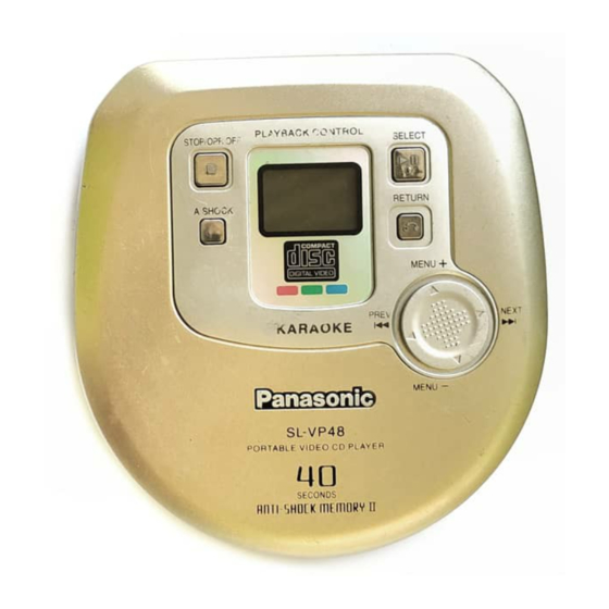
Portable Video CD Player
SL-VP48 / SL-VP43 / SL-VP33
Traverse Deck: RAE0145Z Mechanism Series
Colours
(S)............Silver Type
(N)............Gold Type
Areas
GK..............China.
GH..............Hong Kong.
GCS...........Asia, Latin America, Middle Near East, Africa and Oceania.
SPECIFICATIONS
1
Advertisement
Table of Contents


Need help?
Do you have a question about the SL-VP48 and is the answer not in the manual?
Questions and answers