Table of Contents
Advertisement
Quick Links
Advertisement
Table of Contents

Related Manuals for Asus AAEON EPIC-CFS7-A13-0002


Summary of Contents for Asus AAEON EPIC-CFS7-A13-0002
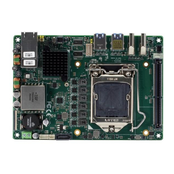
- Page 1 EPIC-CFS7 EPIC Board User’s Manual 1 Last Updated: April 27, 2021...
- Page 2 Copyright Notice This document is copyrighted, 2021. All rights are reserved. The original manufacturer reserves the right to make improvements to the products described in this manual at any time without notice. No part of this manual may be reproduced, copied, translated, or transmitted in any form or by any means without the prior written permission of the original manufacturer.
- Page 3 Acknowledgements All other product names or trademarks are properties of their respective owners. The publisher and writer of this document make no claim to ownership of these products, nor is any claim implied for products not specifically named in this section. Microsoft Windows is a registered trademark of Microsoft Corp.
- Page 4 Packing List Before setting up your product, please make sure the following items have been shipped: Item Quantity EPIC-CFS7 ⚫ Jumper Cap ⚫ Back plate for cooler ⚫ If any of these items are missing or damaged, please contact your distributor or sales representative immediately.
- Page 5 About this Document This User’s Manual contains all the essential information, such as detailed descriptions and explanations on the product’s hardware and software features (if any), its specifications, dimensions, jumper/connector settings/definitions, and driver installation instructions (if any), to facilitate users in setting up their product. Users may refer to the product page at AAEON.com for the latest version of this document.
- Page 6 Safety Precautions Please read the following safety instructions carefully. It is advised that you keep this manual for future references All cautions and warnings on the device should be noted. Make sure the power source matches the power rating of the device. Position the power cord so that people cannot step on it.
- Page 7 If any of the following situations arises, please the contact our service personnel: Damaged power cord or plug Liquid intrusion to the device iii. Exposure to moisture Device is not working as expected or in a manner as described in this manual The device is dropped or damaged Any obvious signs of damage displayed on the device...
- Page 8 FCC Statement This device complies with Part 15 FCC Rules. Operation is subject to the following two conditions: (1) this device may not cause harmful interference, and (2) this device must accept any interference received including interference that may cause undesired operation.
- Page 9 China RoHS Requirements (CN) 产品中有毒有害物质或元素名称及含量 AAEON System QO4-381 Rev.A0 有毒有害物质或元素 部件名称 铅 汞 镉 六价铬 多溴联苯 多溴二苯 醚(PBDE) (Pb) (Hg) (Cd) (Cr(VI)) (PBB) 印刷电路板 × ○ ○ ○ ○ ○ 及其电子组件 外部信号 × ○ ○ ○ ○ ○ 连接器及线材 外壳 ○...
- Page 10 China RoHS Requirement (EN) Hazardous and Toxic Materials List AAEON System QO4-381 Rev.A0 Hazardous or Toxic Materials or Elements Component Name PCB and Components Wires & Connectors for Ext.Connections Chassis CPU & RAM HDD Drive LCD Module Optical Drive Touch Control Module Battery This form is prepared in compliance with the provisions of SJ/T 11364.
-
Page 11: Table Of Contents
Table of Contents Chapter 1 - Product Specifications..................1 Specifications ......................2 Chapter 2 – Hardware Information ..................4 Dimensions ....................... 5 Jumpers and Connectors ..................6 List of Jumpers ......................8 2.3.1 Front Panel PIN Header (JP1) ..............8 2.3.2 AT/ATX mode Selection (JP2) .............. - Page 12 Block Diagram ......................23 Chapter 3 - BIOS Setup ......................24 System Test and Initialization ................25 AMI BIOS Setup ..................... 26 Setup Submenu: Main ..................27 Setup Submenu: Advanced ................. 28 3.4.1 CPU Configuration ..................29 3.4.2 SATA Configuration ................... 30 3.4.3 Hardware Monitor ..................
- Page 13 Memory Address Map ..................57 IRQ Mapping Chart ....................58 Appendix B - Watchdog Timer Programming ..............60 Watchdog Timer Registers ................... 61 Watchdog Sample Program ................62 Preface XIII...
-
Page 14: Chapter 1 - Product Specifications
Chapter 1 Chapter 1 - Product Specifications... -
Page 15: Specifications
Specifications System Form Factor 4” EPIC Board 8th Generation Intel® Core™ Processor family CPU Frequency Up to 4.6GHz Chipset Intel® H310/Q370 (TDP: 6W) Memory Type DDR4 2666 MHz SODIMM x 2 (Dual Channel, Non-ECC) Max. Memory Capacity Up to 32GB BIOS AMI UEFI Wake on LAN... - Page 16 Ethernet Intel® I211, 10/100/1000Base, RJ45 x 2 (Supports PoE 802.3af) *optional RJ45 x 4 supporting PoE 802.3af with daughter board Audio — USB Port USB3.2 Gen 2/ USB2.0 x 4 (Rear I/O) USB2.0 x 2 (Internal header) Serial Port RS-232/422/485 x 2 (Internal header) Parallel Port (printer port) —...
-
Page 17: Chapter 2 - Hardware Information
Chapter 2 Chapter 2 – Hardware Information... -
Page 18: Dimensions
Dimensions Chapter 2 – Hardware Information... -
Page 19: Jumpers And Connectors
Jumpers and Connectors Chapter 2 – Hardware Information... - Page 20 Chapter 2 – Hardware Information...
-
Page 21: List Of Jumpers
List of Jumpers Please refer to the table below for all of the board’s jumpers that you can configure for your application. Label Function Front Panel PIN Header AT/ATX Mode Selection Clear C-MOS PIN Header 2.3.1 Front Panel PIN Header (JP1) Signal Description Signal Description EXT_PWRBTN#... -
Page 22: At/Atx Mode Selection (Jp2)
2.3.2 AT/ATX mode Selection (JP2) ATX Mode AT mode (Default) 2.3.3 Clear CMOS Jumper (JP3) Normal (Default) Clear CMOS Chapter 2 – Hardware Information... -
Page 23: List Of Connectors
List of Connectors The table below lists all of the board’s connectors, configurable for your application. Label Function LPC connector for debug SATA connector SATA Power connector 2 PIN DC IN connector DIO Power connector PCIe [X4] FPC connector CN10 CPU Fan connector CN11 POE LAN RJ45 connector... -
Page 24: Lpc Port (Cn1)
2.4.1 LPC Port (CN1) Signal Description Signal Description LPC_AD0 RST# LPC_AD1 LPC_AD2 LPC_AD3 I2C0_data/SMB_data P3V3 I2C0_CLK/SMB_CLK FRAME# INT_SERIRQ Chapter 2 – Hardware Information... -
Page 25: Sata Connector (Cn2)
2.4.2 SATA Connector (CN2) Signal Description Signal Description SATA_RXN0 SATA_TXP0 SATA_RXP0 SATA_TXN0 2.4.3 SATA Power (CN4) Signal Description +5V max 1A Chapter 2 – Hardware Information... -
Page 26: Pin Dc In Connector (Cn5)
2.4.4 2 Pin DC IN Connector (CN5) +VIN GND Signal Description +12V 2.4.5 DIO Power Connector (CN6) Signal Description +V5S max 0.5A +V3P3S max 1A Chapter 2 – Hardware Information... -
Page 27: Pcie [X4] Fpc Connector (Cn9)
2.4.6 PCIe [x4] FPC Connector (CN9) Signal Description Signal Description +V3P3S PCIE_12_TXN +V3P3S PCIE_12_TXP +V3P3S SMB_DATA PCIE_11_TXN SMB_CLK PCIE_11_TXP BUF_PLT_RST# +V3P3A PCIE_10_TXN PCIE_10_TXP PCIE_10_RXP PCIE_10_RXN PCIE_3_CLK_DN PCIE_3_CLK_DP PCIE_12_RXP PCIE_12_RXN PCIE_9_TXN PCIE_9_TXP PCIE_11_RXP PCIE_11_RXN +V12V +V12V PCIE_9_RXP +V12V PCIE_9_RXN +V12V +V12V Chapter 2 –... -
Page 28: Cpu Fan Connector (Cn10)
2.4.7 CPU FAN Connector (CN10) Signal Description FAN_POWER (max 1A) FAN_TAC FAN_CTL 2.4.8 POE LAN (RJ-45) Connector (CN11) Signal Description Signal Description LAN2_MDI0_N LAN2_LED_100# LAN2_MDI0_P LAN2_LED_1000# LAN2_MDI1_N AGND LAN2_MDI1_P OUT2_LED LAN2_MDI2_N LAN2_MDI2_P LAN2_MDI2_N LAN2_MDI3_P R11A OUT2 R10A R12A AGND LAN1_MDI0_N LAN1_LED_100# LAN1_MDI0_P LAN1_LED_1000#... -
Page 29: Rs232/422/485 Connector Com1, Com2 (Cn12/13)
Signal Description Signal Description LAN1_MDI1_N AGND LAN1_MDI1_P OUT1_LED LAN1_MDI2_N LAN1_MDI2_P LAN1_MDI3_N LAN1_MDI3_P R11B OUT1 R10B R12B AGND 2.4.9 RS232/422/485 connector COM1, COM2 (CN12/13) RS232 Signal Description Signal Description DCD2 CTS2 DSR2 DTR2 RTS2 Chapter 2 – Hardware Information... - Page 30 RS422 Signal Description Signal Description RS422_TX2- RS422_RX2- RS422_TX2+ NC/+5V/+12V max 0.5A RS422_RX2+ RS485 Signal Description Signal Description RS485_ D2- RS485_D2+ NC/+5V/+12V max 0.5A Chapter 2 – Hardware Information...
-
Page 31: Hdmi Connector (Cn14/15)
2.4.10 HDMI Connector (CN14/15) Signal Description Signal Description HDMI_TX2+ HDMI_CLK- HDMI_TX2- HDMI_TX1+ DDC_CLK HDMI_TX1- DDC_DATA HDMI_TX0+ HDMI_TX0- HDMI_HPD HDMI_CLK+ Chapter 2 – Hardware Information... -
Page 32: Usb 3.2 Gen 2 Connector (Cn16)
2.4.11 USB 3.2 Gen 2 Connector (CN16) Signal Description Signal Description +5VSB +5VSB USB1_D- USB2_D- USB1_D+ USB2_D+ USB1_SSRX− USB2_SSRX− USB1_SSRX+ USB2_SSRX+ USB1_SSTX− USB2_SSTX− USB1_SSTX+ USB2_SSTX+ Chapter 2 – Hardware Information... -
Page 33: Usb 3.2 Gen 2 Connector (Cn17)
2.4.12 USB 3.2 Gen 2 Connector (CN17) Signal Description Signal Description +5VSB +5VSB USB3_D- USB4_D- USB3_D+ USB4_D+ USB3_SSRX− USB4_SSRX− USB3_SSRX+ USB4_SSRX+ USB3_SSTX− USB4_SSTX− USB3_SSTX+ USB4_SSTX+ 2.4.13 RTC Connector (CN18) Signal Description RTCVCC Chapter 2 – Hardware Information... -
Page 34: Usb 2.0 Connector (Cn19)
2.4.14 USB 2.0 Connector (CN19) Signal Description Signal Description USBD- USBD- USBD+ USBD+ 2.4.15 Mini-Card Connector (CN20) Signal Description Signal Description PCIE_WAKE# +3.3VSB +1.5V SMB_CLK PCIE_TX- +1.5V SMB_DATA PCIE_TX+ UIM_PWR UIM_DATA USB_D- PCIE_REF_CLK- Chapter 2 – Hardware Information... -
Page 35: Ddr4 So-Dimm Slot (Dimm1 & Dimm2)
Signal Description Signal Description UIM_CLK USB_D+ PCIE_REF_CLK+ +3.3VSB UIM_RST +3.3VSB UIM_VPP W_DISABLE# PCIE_RST# +1.5V PCIE_RX- +3.3VSB PCIE_RX+ +3.3VSB 2.4.16 DDR4 SO-DIMM Slot (DIMM1 & DIMM2) Standard specification Chapter 2 – Hardware Information... -
Page 36: Block Diagram
Block Diagram Chapter 2 – Hardware Information... -
Page 37: Chapter 3 - Bios Setup
Chapter 3 Chapter 3 - BIOS Setup... -
Page 38: System Test And Initialization
System Test and Initialization The EPIC-CFS7 board uses certain routines to test and initialize board hardware. If the routines encounter an error during the tests, you will either hear a few short beeps or see an error message on the screen. There are two kinds of errors: fatal and non-fatal. The system can usually continue the boot up sequence with non-fatal errors. -
Page 39: Ami Bios Setup
AMI BIOS Setup AMI BIOS ROM has a built-in Setup program that allows users to modify the basic system configuration. This information is stored in a battery-backed CMOS RAM and BIOS NVRAM so that it retains the Setup information when the power is turned off. To enter setup, power on the computer and press <Del>or <ESC>... -
Page 40: Setup Submenu: Main
Setup Submenu: Main Chapter 3 – BIOS Setup... -
Page 41: Setup Submenu: Advanced
Setup Submenu: Advanced Chapter 3 – BIOS Setup... -
Page 42: Cpu Configuration
3.4.1 CPU Configuration Options Summary Active Processor Cores Optimal Default, Failsafe Default Number of cores to enable in each processor package. Intel (VMX) Virtualization Disabled Technology Enabled Optimal Default, Failsafe Default When enabled, a VMM can utilize the additional hardware capabilities provided by Vanderpool Technology. -
Page 43: Sata Configuration
3.4.2 SATA Configuration Options Summary SATA Controller(s) Disabled Enabled Optimal Default, Failsafe Default Enable/Disable SATA Device. Port 0 Disabled Optimal Default, Failsafe Default Enabled Enable or Disable SATA Port mSATA port Disabled Enabled Optimal Default, Failsafe Default Enable or Disable SATA Port Chapter 3 –... -
Page 44: Hardware Monitor
3.4.3 Hardware Monitor Chapter 3 – BIOS Setup... -
Page 45: Smart Fan Mode Configuration
3.4.3.1 Smart Fan Mode Configuration Auto Duty-Cycle Mode Options Summary FAN1 Output Output PWM mode (open drain) Mode Linear Fan Application Output PWM mode (push pull) Optimal Default, Failsafe Default Output PWM mode (push pull) to control 4-wire fans. Linear fan application circuit to control 3-wire fan speed by fan’s power terminal. Output PWM mode (open drain) to control Intel 4-wire fans. - Page 46 Auto RPM Mode Options Summary RPM Percentage Auto fan speed control. Fan speed will follow different temperature by different RPM 1-100 Temperature Chapter 3 – BIOS Setup...
- Page 47 Manual Duty Mode Options Summary Manual Duty Mode Optimal Default, Failsafe Default Manual mode fan control, user can write expected duty cycle (PWM fan type) 1-100 Chapter 3 – BIOS Setup...
-
Page 48: Sio Configuration
3.4.4 SIO Configuration Chapter 3 – BIOS Setup... -
Page 49: Serial Port 1 Configuration
3.4.4.1 Serial Port 1 Configuration Options Summary Use This Device Disable Enable Optimal Default, Failsafe Default Enable or Disable this Logical Device. Possible: Use Automatic Settings Optimal Default, Failsafe Default IO=3F8h; IRQ=4 IO=2F8h; IRQ=3 Allows user to change Device's Resource settings. New settings will be reflected on This Setup Page after System restarts. -
Page 50: Serial Port 2 Configuration
3.4.4.2 Serial Port 2 Configuration Options Summary Use This Device Disable Enable Optimal Default, Failsafe Default Enable or Disable this Logical Device. Possible: Use Automatic Settings Optimal Default, Failsafe Default IO=2F8h; IRQ=3 IO=3F8h; IRQ=4 Allows user to change Device's Resource settings. New settings will be reflected on This Setup Page after System restarts. -
Page 51: Power Management
3.4.5 Power Management Options Summary Power Mode ATX Type Optimal Default, Failsafe Default AT Type Select system power mode Restore AC Power Last State Optimal Default, Failsafe Default Loss Always On Always Off IO Restore AC power Loss RTC wake system from Disable Optimal Default, Failsafe Default Fixed Time... -
Page 52: Digital Io Port Configuration
3.4.6 Digital IO Port Configuration Options Summary DIO Port* Output Input Set DIO as Input or Output Output Level High Optimal Default, Failsafe Default Set output level when DIO pin is output Chapter 3 – BIOS Setup... -
Page 53: Setup Submenu: Chipset
Setup Submenu: Chipset Chapter 3 – BIOS Setup... -
Page 54: System Agent (Sa) Configuration
3.5.1 System Agent (SA) Configuration Chapter 3 – BIOS Setup... -
Page 55: Pch-Io Configuration
3.5.2 PCH-IO Configuration Options Summary HD Audio Disabled Enabled Optimal Default, Failsafe Default Control Detection of the HD-Audio device. Disabled = HDA will be unconditionally disabled Enabled = HDA will be unconditionally enabled. MiniCard Slot Function SATA Optimal Default, Failsafe Default PCIe Select function enabled for Half-MiniCard (CN20) slot Chapter 3 –... -
Page 56: Setup Submenu: Security
Setup Submenu: Security Change User/Administrator Password You can set an Administrator Password or User Password. An Administrator Password must be set before you can set a User Password. The password will be required during boot up, or when the user enters the Setup utility. A User Password does not provide access to many of the features in the Setup utility. -
Page 57: Secure Boot
3.6.1 Secure Boot Options Summary Secure Boot Disabled Optimal Default, Failsafe Default Enabled Secure Boot feature is Active if Secure Boot is Enabled, Platform Key(PK) is enrolled and the System is in User mode. The mode change requires platform reset Secure Boot Mode Custom Optimal Default, Failsafe Default... -
Page 58: Key Management
3.6.1.1 Key Management Options Summary Factory Key Provision Disabled Optimal Default, Failsafe Default Enabled Secure Boot feature is Active if Secure Boot is Enabled, Platform Key(PK) is enrolled and the System is in User mode. The mode change requires platform reset Restore Factory Keys Force System to User Mode. - Page 59 Options Summary Restore DB defaults Restore DB variable to factory defaults Platform Key(PK) Details Export Update Delete Key Exchange Keys Details Export Update Append Delete Authorized Signatures Details Export Update Append Delete Forbidden Signatures Details Export Update Append Delete Authorized TimeStamps Update Append OsRecovery Signatures...
-
Page 60: Setup Submenu: Boot
Setup Submenu: Boot Options Summary Quiet Boot Disabled Enabled Optimal Default, Failsafe Default Enable or disable showing boot logo. Lunch PXE ROM Disabled Optimal Default, Failsafe Default Enabled Controls the execution of UEFI and Legacy Network OpROM Chapter 3 – BIOS Setup... -
Page 61: Bbs Priorities
3.7.1 BBS Priorities Chapter 3 – BIOS Setup... -
Page 62: Setup Submenu: Save & Exit
Setup Submenu: Save & Exit Chapter 3 – BIOS Setup... -
Page 63: Chapter 4 - Driver Installation
Chapter 4 Chapter 4 – Driver Installation... -
Page 64: Driver Installation
Driver Installation Drivers for the EPIC-CFS7 can be downloaded from the product page on the AAEON website by following this link: https://www.aaeon.com/en/p/epic-boards-epic-cfs7 Download the driver(s) you need and follow the steps below to install them. Before beginning installation, use the following chart to determine if your operating system (OS) is compatible with the drivers AAEON provides for the EPIC-CFS7. - Page 65 Step 2 – Install Graphics Drivers Open the Step 2 - Graphic folder Open the win64_25.20.100.6373.exe file in the folder Follow the instructions Drivers will be installed automatically Step 3 – Install Network Drivers Open the Step 3 – Network folder Open the ProWinx64.exe file in the folder Follow the instructions Drivers will be installed automatically...
-
Page 66: Appendix A - I/O Information
Appendix A Appendix A - I/O Information... -
Page 67: I/O Address Map
I/O Address Map Appendix A – I/O Information... - Page 68 Appendix A – I/O Information...
- Page 69 Appendix A – I/O Information...
-
Page 70: Memory Address Map
Memory Address Map Appendix A – I/O Information... -
Page 71: Irq Mapping Chart
IRQ Mapping Chart Appendix A – I/O Information... - Page 72 Appendix A – I/O Information...
-
Page 73: Appendix B - Watchdog Timer Programming
Appendix B Appendix B - Watchdog Timer Programming... -
Page 74: Watchdog Timer Registers
Watchdog Timer Registers Table 1 : Watch dog relative IO address Default Value Note I/O Base I/O Base address for Watchdog operation. 0x2E Address This address is assigned by SIO LDN7 Table 2 : Watchdog relative register table Register Offset BitNum Value Note... -
Page 75: Watchdog Sample Program
Watchdog Sample Program ****************************************************************************** // WDT I/O operation relative definition (Please reference to Table 1) #define WDTAddr 0x510 // WDT I/O base address Void WDTWriteByte(byte Register, byte Value); byte WDTReadByte(byte Register); Void WDTSetReg(byte Register, byte Bit, byte Val); // Watch Dog relative definition (Please reference to Table 2) #define DevReg 0x00 // Device configuration register #define WDTRstBit 0x80 // Watchdog WDTRST# (Bit7) - Page 76 ******************************************************************************* // Procedure : AaeonWDTEnable VOID EnterSIOconfig IOWriteByte (IoConfAddr,0x87); IOWriteByte (IoConfAddr,0x87); VOID ExitSIOconfig IOWriteByte (IoConfAddr,0xAA); VOID SetWDT IOWriteByte (IoConfAddr,0x2B); IOWriteByte(IoConfAddr+1, (IOReadByte(IoConfAddr+1)&0xFC)); // Procedure : AaeonWDTEnable AaeonWDTEnable () VOID WDTEnableDisable(1); // Procedure : AaeonWDTConfig AaeonWDTConfig (byte Counter, BOOLEAN Unit) VOID // Disable WDT counting WDTEnableDisable( // Clear Watchdog Timeout Status WDTClearTimeoutStatus();...
- Page 77 WDTSetBit( TimerReg, UnitBit, Unit // WDT output mode set to pulse WDTSetBit( TimerReg, ModeBit, ModeVal // WDT output mode set to active low WDTSetBit( TimerReg, PolarityBit, PolarityVal // WDT output pulse width is 25ms WDTSetBit( TimerReg, PSWidthBit, PSWidthVal // Watchdog WDTRST# Enable WDTSetBit( DevReg, WDTRstBit, WDTRstVal WDTClearTimeoutStatus()
Need help?
Do you have a question about the AAEON EPIC-CFS7-A13-0002 and is the answer not in the manual?
Questions and answers