Advertisement
Quick Links
Service Manual
. Technical Specifications.........................................................1-2
. Safety Instruction, Warning & Notes........................................1-3
. Mechanical and Dismantling Instructions....................................2-1
. Software Upgrades and Region Code Change.............................
. Trouble Shooting Chart......................................................
. Wiring Diagram..................................................................5-1
. Electrical Diagrams and Print-layouts......................................6-1
. Set Mechanical Exploded view & Part list................................7-1
. Revision List..................................................................................8-1
©Copyright 2010 Philips Consumer Electronics B.V. Eindhoven, The Netherlands
All rights reserved. No part of this publication may be reproduced, stored in aretrieval system or
transmitted, in any form or by any means, electronic, mechanical, photocopying, or otherwise
without the prior permission of Philips.
Published by SL - 009 BU AVM
Version 1.2
TABLE OF CONTENTS
Printed in The Netherlands
Subject to modification
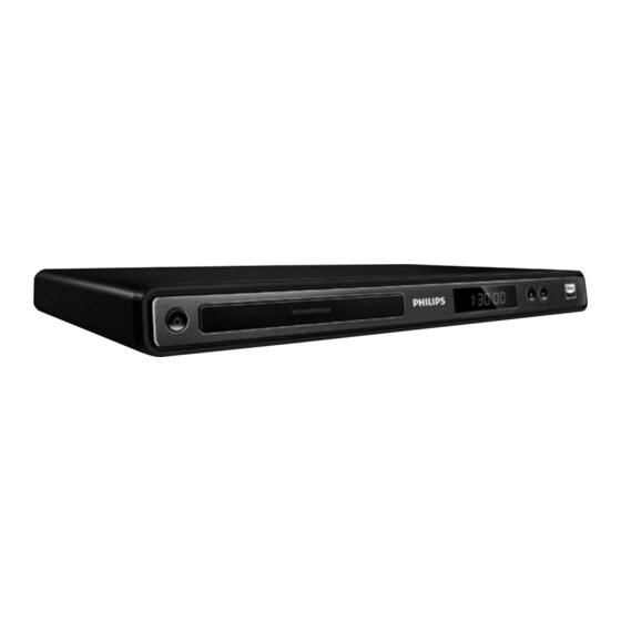
DVP352X(K)
DVP3520/55
DVP3522/55
DVP3520K/93
Page
3-1
.
4-1
.
CLASS 1
LASER PRODUCT
3141 785 34562
GB
PHILIPS
Advertisement

Subscribe to Our Youtube Channel
Related Manuals for Philips DVP352X


Summary of Contents for Philips DVP352X
-
Page 1: Table Of Contents
. Electrical Diagrams and Print-layouts..….…………………..….…6-1 . Set Mechanical Exploded view & Part list.…………………..….….7-1 . Revision List..................8-1 ©Copyright 2010 Philips Consumer Electronics B.V. Eindhoven, The Netherlands All rights reserved. No part of this publication may be reproduced, stored in aretrieval system or CLASS 1... -
Page 2: Technical Specifications
• Specifications are indicative (subject to change). Technical Specifications For on-line product support please use the following website: http://www.p4c.philips.com/cgi-bin/dcbint/cpproduct_selector.pl Here is product information available, as well as getting started, user manuals, frequently asked questions and software & drivers. Directions for Use You can download this information from the following websites: http://www.philips.com/support... - Page 3 Make sure that, • Use only lead-free soldering tin Philips SAC305 with order during repair, you are connected with the same potential as code 0622 149 00106. If lead-free solder paste is required, the mass of the set by a wristband with resistance.
- Page 4 1 - 4 Safety Instructions, Warnings, Notes, and Abbreviation List Abbreviation List 2.3.5 Alternative BOM identification It should be noted that on the European Service website, 0/6/12 SCART switch control signal on A/V “Alternative BOM” is referred to as “Design variant”. board.
- Page 5 Electro Magnetic Interference LORE LOcal REgression approximation EPLD Erasable Programmable Logic Device noise reduction Europe LG.Philips LCD (supplier) EXTernal (source), entering the set by Loudspeaker SCART or by cinches (jacks) LVDS Low Voltage Differential Signalling Fast BLanking: DC signal Mbps...
- Page 6 4.406250 MHz and 4.250000 MHz Sound Intermediate Frequency SMPS Switched Mode Power Supply System on Chip Sync On Green SOPS Self Oscillating Power Supply S/PDIF Sony Philips Digital InterFace SRAM Static RAM Service Reference Protocol Small Signal Board STBY STand-BY SVGA 800x600 (4:3)
-
Page 7: Mechanical And Dismantling Instructions
Mechanical and Dismantling Instructions Dismantling Instruction Detailed information please refer to the model set. The following guidelines show how to dismantle the player. Step1: Remove 5 screws around the Top Cover, and then remove the Top Cover (Figure 1). Figure 1 Step2: If it is necessary to dismantle Loader or Front Panel, the Front door should be removed first. - Page 8 Mechanical and Dismantling Instructions Detailed information please refer to the model set. Dismantling Instruction Step3: If the tray can’t open in normal way, you can make it through the instruction as below (Figure 3). Note: Make sure to operate gently otherwise the guider would be damaged. Figure 3 Step4: Dismantling Front Panel, disconnect the connectors (XS30 1), need release 4 snaps of Front Panel &...
- Page 9 Mechanical and Dismantling Instructions Dismantling Instruction Detailed information please refer to the model set. Step5: Dismantling Loader, disconnect the 3 connectors (XP2, XP3, XP4) aiming in the below figure, and remove 1 screw that connects the loader and the bottom cabinet. (Figure 5) Figure 5 Step6: Dismantling Main Board, first disconnect the connector (XP1), and then remove 4 screws.
-
Page 10: Software Upgrades And Region Code Change
Softeware upgrade and region code change Preparation to upgrade software 1) Power on the set and open the tray, then press "5""5" B. Read out the software versions to confirm upgrading on remote control to check the SW File Name. 2) Start the CD Burning software and create a new CD Power on the set and press "Setup"... -
Page 11: Trouble Shooting Chart
Trouble shooting chart Spindle motor does not move Motor no move Check the FFC connection Correct connection between 24P and the loader. Check whether “M5V” Check the M5V power supply (+5V) voltage is normal. Check whether laser voltage Check/Replace Q103,Q104. (1.9V for CD &... - Page 12 Trouble shooting chart The power can not be on or off The power can’t be on or off Check the power supply Repair the power board on the power board is normal. Check if the XS301 on the front board to XP5 on the Check/Correct connection decoder board is in good contact.
- Page 13 Trouble shooting chart All output voltages on the power board is 0V or deviated. All output voltages on the power board is 0V or deviated Check whether Replace F501 F501 is blown Replace C501&C502 if D501, D502, Check whether there is D503, D504 are normal.
- Page 14 Trouble shooting chart Disc cannot be read . Disc cannot be read. Check the FFC connection Check the loaded circuit between 24P and the loader. 1. Whether voltage on pin102/pin103 of U1 varies between 2.4V 3.3V Check whether there is laser (Pin102=3.3V and Pin103=2.4V for CD;...
- Page 15 Trouble shooting chart Only DVD disc or only disc except DVD can be played Only DVD disc, or only disc except DVD can be Played. Check connection between Check the loaded circuit 24pin and the loader. Check whether there is laser Check the solder status on U1 and voltage (1.9V for CD and 2.4V peripheral components...
- Page 16 Trouble shooting chart No display on LED, and buttons do not work No display on LED, and buttons do not work Check whether there is correct contact Correct connection between XS301 and Fix power supply board top Check VCC(M5V) voltage a power supply for should on the power and front electric circuit...
- Page 17 Trouble shooting chart Distorted audio and loud noise Distorted audio and loud noise Check the power supply voltages Check Q544 operation amplifying Q544 is normal. Check whether the muting Replace R369,R375 resistance R369,R375 are normal Check whether the muting Replace transistor Q361,Q362 are Q361,Q362 normal...
- Page 18 Trouble shooting chart Abnormal color of video picture Abnormal color of video picture Check whether Check Y1, R10,R11,C10 and C11 27MHz output signal Check whether the 3.3V Check other of power supply electric and 1.2V power supply circuit voltages on the decoder board are normal.
- Page 19 Trouble shooting chart Remote reception is insensitive or fails. Remote reception is insensitive or fails. Check if the remote Check battery control works properly. Check power Check R315 C315 supply voltage to the remote censor is normal Use an oscilloscope to check if there is output waveform from the first pin IR of the remote censor REM301(PIN1 - RC waveform)
- Page 20 4-10 Trouble shooting chart No video picture, no sound. No video picture, no sound. CVBS(R21 point) waveform Check whether all the voltages Check the loaded circuit from the power board to the decoder board are normal. Check if the reset circuit consisting of CE2, D1,Q1 is normal (at a low level Change CE2, D1,Q1.
- Page 21 SPHE8202R-D(2ch) WIRING DIAGRAM COAX CVBS AUDIO AMP&LPF VIDEO LPF POWER SUPPLY TNY176 +P12V M+5V SPHE8202R-D XS201 M+5V 5PIN*2.5 HOMESW FLASH LOAD- EN25T16 LOAD+ OUTSW 5PIN*2.0 INSW 6PIN*2.0 4PIN*2.0 MAIN BOARD USB_DM USB_DP XS301 6PIN*2.0 XP303 XS302 XS601 SWITCH KS6S 4PIN*2.0 KEY2 LED+ 4PIN*2.0...
- Page 22 SPHE8202RQ-D(2ch) WIRING DIAGRAM DVP3520K COAX CVBS AUDIO AMP&LPF VIDEO LPF POWER SUPPLY TNY176 +P12V M+5V SPHE8202RQ-D XS201 3PIN*2.5 HOMESW FLASH LOAD- EN25T16 LOAD+ OUTSW 5PIN*2.0 INSW 6PIN*2.0 3PIN*2.0 XP476 MAIN BOARD +12VA XS301 6PIN*2.0 XP303 XS302 XP601 SWITCH KS6S 3PIN*2.0 KEY2 LED+ 4PIN*2.0...
- Page 23 47uF 47uF XS301 XS301 C316 C316 C307 C307 C308 C308 100p 100p 100p 100p 100p 100p R320 R320 for dvp352x DATA DATA POWER_K STB_LED R303 R303 R304 R304 R305 R305 R319 R319 0 ohm 0 ohm LED- CON10(2.0) CON10(2.0) R306...
- Page 24 Switch Board Circuit Diagram: K303 K303 POWER POWER LED3 LED3 CON4(2.0) CON4(2.0) C319 C319 C317 C317 C318 C318 SWITCH BOARD...
- Page 25 OK Board & USB Board Electric Diagram (Only for DVP3522 and has not karaoke output) R210 12VA R202 12VA C201 CE200 CE201 0.1u 22uF 22uF R203 C205 R205 180K P601 R211 KARAOKE INPUT C210 R201 U200A C211 100K 5.6K 2.2uF 2.2uF R200 C203...
- Page 26 OK Board Circuit Diagram for DVP3520K/93: R210 R210 12VA R202 R202 12VA C201 C201 CE200 CE200 CE201 CE201 0.1u 0.1u 22uF 22uF R203 R203 22uF 22uF C205 C205 R205 R205 180K 180K P601 P601 R211 R211 KARAOKE INPUT KARAOKE INPUT C210 C210 R201...
- Page 27 R507 1/6W11.3k 1% 1/6W11.3k 1% CY501 CY501 102/400Vac 102/400Vac * No use the Class 1 environment management materials of SS-00259 * All of moulding resinous, ink, paint and coating electric wire must be ordered from designated GP supplier of Philips.
- Page 28 Main Board Circuit Diagram: POWER & MOTOR DRIVER R761 R761 TO POWER BOARD 1.8/2W 1.8/2W R751 R751 NM/0 NM/0 Inor=155mA Imax=???mA Istandby:8mA 5pin/2.5mm 5pin/2.5mm R762 10/1W R762 10/1W C753 C753 Q753 Q753 SS8550D SS8550D 50mA Q762 Q762 C752 C752 C751 C751 R753 R753...
- Page 29 Main Board Circuit Diagram: SPHD8202R-D modify DV33 FV33 Crystal 4.7K 4.7K M_D[0..15] DQ[0..15] 4pin/2.0mm 4pin/2.0mm TP11 TP11 M_A[0..11] 10uF16V 10uF16V MA[0..11] URST# M_DQM[0..1] URST# DQM[0..1] 27MHz 27MHz 33pF 33pF M_BA[0..1] 33pF 33pF BA[0..1] C251 C251 C252 C252 NM/15pF NM/15pF C253 C253 RAM_CLK DCLK...
- Page 30 Main Board Circuit Diagram: SDRAM&FLASH SD33 DQ[0..15] DQ[0..15] platform Not 89S MA[0..11] MA[0..11] R194 Open Close BA[0..1] BA[0..1] DQM[0..1] DQM[0..1] C186 C186 C187 C187 C188 C188 +CE186 +CE186 R195 Open Close DCLK DCLK 47uF16V 47uF16V C189 C189 0.1uF 0.1uF 0.1uF 0.1uF 0.1uF 0.1uF...
- Page 31 Main Board Circuit Diagram: AUDIO I/F For 6CH and without optical output model AUDIO_MUTE AUDIO_MUTE SPDIF SPDIF P441 P441 RCA/AUDIO OUT RCA/AUDIO OUT COAXIAL AUDIO I/F 27K 1% 27K 1% R366 R366 C443 C443 C441 C441 1000pF 1000pF 6CH Audio AMP for single input SUNPLUS. C365 C365 120pF...
- Page 32 Main Board Circuit Diagram: VIDIO I/F V_CVBS V_CVBS V_G/Y V_G/Y V_B/U V_B/U V_R/V V_R/V VIDEO I/F VIDEO OUTPUT TERMINAL. L881 L881 0R/1.8uH 0R/1.8uH V_R/V R/V_O RCA/VIDEO OUT RCA/VIDEO OUT R881 R881 C881 C881 75R 1% 75R 1% 100pF 100pF CVBS_O G/Y_O C926 C926...
- Page 33 6-10 6-10 Main Board Circuit Diagram: OTHER & USB & KOK PBSS5320 PBSS5320 F221 F221 FUSE(500MA) FUSE(500MA) Q221 Q221 R221 R221 USB_CON R222 R222 VCC_USB USB_DM USB_DP C221 C221 Karaoke input interface with MPEG IC,for ZORAN platforms. USB CONNECTOR USB CONNECTOR 0.1uF 0.1uF U221 PRTR5V0U2X...
- Page 34 7-11 7-11 Front Board and Switch Board Print-layout (Bottom side): OK Board Print-layout for DVP3520K/93 (Bottom side):...
- Page 35 6-12 6-12 USB Board Print-layout (Top side) USB Board Print-layout (Bottom side): Remark: Only for DVP3522 and has not karaoke output.
- Page 36 6-13 6-13 Power Board Print-layout (Bottom side):...
- Page 37 6-14 6-14 Main Board Print-layout (Top side):...
- Page 38 6-15 6-15 Main Board Print-layout (Bottom side):...
- Page 39 Exploded View for DVP3520/55: It is a general mechanical exploded view for DVP3520/55, pls refer to the model set for detailed information. ASSY1 includes components:1.3.4.5.20...
- Page 40 Exploded view for DVP3522/55: It is general mechanical exploded view for DVP3522/55, pls refer to model set for detailed information. ASSY1 includes components:1.3.4.5.22...
- Page 41 Exploded view for DVP3520K/93: It is general mechanical exploded view for DVP3520K/93, pls refer to model set for detailed information. ASSY1 includes components:1.3.4.5.21...
- Page 42 DVP3520/55 SERVICE PARTLIST ELECTRICAL PARTLIST MECHANICAL PARTLIST 12NC No. Description Q'ty 12NC No. Description Q'ty 996510031325 ASSY-MAIN BD 996510031317 TOP CABINET 996510031326 ASSY-PW BD 996510001175 POWER CORD 996510031321 ASSY-FB BD (+SW BD) 996510031323 BACK PANEL 996510031324 ASSY-SW BD (+FB BD) 996510006463 996510031315 LOADER...
- Page 43 DVP3522/55 SERVICE PARTLIST ELECTRICAL PARTLIST ASSY-FB BD COMPONENT PARTLIST 12NC No. Description Q'ty 12NC NO. Description Q'ty 996510031885 ASSY-MAIN BOARD LED1 996510020917 J2808AG 996510031883 ASSY-POWER BOARD REM301 996510020925 HM338-12 RECEIVER MOD H=12MM 996510031876 ASSY-USB BOARD U301 996510009665 IC ET6202 SOP-2 996510031321 ASSY-FB BD (+SW BD) 996510031324...
- Page 44 DVP3520K/93 SERVICE PARTLIST ELECTRICAL PARTLIST ASSY-OK+USB BD COMPONENT PARTLIST 12NC No. Description Q'ty 12NC NO. Description Q'ty 996510034192 ASSY-MAIN BOARD 996500032494 IC AS4558M 996510034193 ASSY-POWER BOARD 996510034184 ASSY-OK+USB BOARD ASSY-FB BD COMPONENT PARTLIST 996510031321 ASSY-FB BD (+SW BD) 12NC NO. Description Q'ty 996510031324...
-
Page 45: Revision List
REVISION LIST Version 1.0 * Initial release for DVP3520/55 Version 1.1 * Adding DVP3522/55 Version 1.2 * Adding DVP3520K/93...
Need help?
Do you have a question about the DVP352X and is the answer not in the manual?
Questions and answers