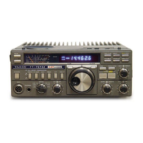
Yaesu FT-757GX Technical Supplement
Hide thumbs
Also See for FT-757GX:
- Supplement manual (97 pages) ,
- Operating manual (73 pages) ,
- Manual (39 pages)

Related Manuals for Yaesu FT-757GX


Summary of Contents for Yaesu FT-757GX
- Page 2 Este manual original foi gentilmente cedido para ser digitalizado por PY2TKI Marcos Digitalizado em 23 de Novembro de 2020 por Alexandre "Tabajara" Souza, PU2SEX http://www.tabalabs.com.br http://tabajara-labs.blogspot.com MANUAL DE DISTRIBUIÇÃO GRATUITA - Respeite o meu esforço de preservar a documentacao...
- Page 3 CONTENTS (Page) ERRATA FOR THE FT-757GX OPERATING MANUAL ......SOLDERING AND DESOLDERING TECHNIQUE .
- Page 5 The in formation stating otherwise on pages 13 (KEYER switch description), 20 ( MANUAL KEY The KEY jack on the rear panel o f the FT-757GX Plug drawing), and 28 (middle o f second paragraph will only accept a 3-conductor phone plug for...
- Page 6 S OLDE R I N G A N D DES OLDE R I N G TECH N I QU E The FT-757GX circuit boards are tough, but mis NOTES ON USE OF CMOS COMPONENTS: handling during soldering can cause circuit traces to "lift."...
- Page 7 EXAMPLES OF POOR SOLDERING PRACTICE BASIC SOLDER I NG PRACTICE Prepare soldering iron and solder. The tip of the iron Unwanted solder bridge con- should thoroughly necting two tracks (caused by use of too much solder) tinned and wiped clean of excess solder .
- Page 8 TYPICAL PART FAILURES, CAUSES AND SYMYl'OMS PARTS CAUSE OF TROUBLE SYMPTOMS Semiconductors High supply voltage Short or open circuit (IC, FET, TR) Open circuit Output decreases to 1/2 at 80°C Excessive drive Internal noise High temperature Instab MOS FET Static electricity Total failure MOS IC Short or open circuit...
- Page 9 Also, be fore making any modification, check to see the end o f the blue wire removed from the i f it has already been carried out by a Yaesu agent, lOO W PA Unit, and then carefully insulate the dealer or previous owner.
- Page 10 . . � J6003/P42 06010 J6004/P48 Component side IOOWPA UNIT (Bl u e) From LOCAL UNIT Component side RF UNIT - 7 -...
- Page 11 CW filter during jumper to the cathode o f diode D 1 0 6 4 (near CW-N reception with the FT-757GX. The cause o f VR1 0 0 3 ). The cathode lead o f this diode is the this problem is insu fficient isolation within F M upper (exposed) lead.
- Page 12 . Softw are computer to control the memory and operating is provi ded with some of the Yaesu Interf ace frequency functions of the transceiver. Control Units when they are design ed for use with one signals are passed to the transceiver on a serial data specif ic micro comp uter.
- Page 13 be inspected bef o re the command is sent to the As illustrated in the Frequency Enter Command example, frequency parameter data is sent least transceiver again. Note that the controls on the significant digit first. The Frequency Step Com transceiver are not disabled when exerc1smg ("f/J(/J") mand example shows how dummy data...
- Page 15 SER VICE A N D A L I GN ME N T The FT-757GX is carefully designed to allow the The f o llowing test equipment (and thorough knowledgeable operator to make all adjustments familiarity with its use) is required for complete required for various station conditions, modes and alignment.
- Page 16 DC milliammeter ranging to 500 mA Linear detector for 1 -30 MHz X-Y oscilloscope with 60 MHz bandwidth 1-.l PA UNIT 100W KEYER UNIT FT-757GX Underside of Heatsink LOCAL UNIT Chassis Top View Chassis Bottom View - 1 3 -...
- Page 17 ALIGN MENT the frequencies shown on the counter are LOCAL Unit within 990 Hz ±5 Hz. A. Third LO BPF H. Carrier Point Remove P1 7 and connect a 50-ohm load across 3rd Connect the frequency counter to J 2008 and LO OUT jack J 2008, along with the RF voltmeter.
- Page 18 V R 2oos V R 2010 V R 2007 V R 2011 T P 2007 V R 2006 (T 2 o 4 -T 2 o T 2004, T 2003 T 201s-T 2021 T 2005 (T2012 , T2010 J2009 T2011,T2009 T C 2005 L2011 T P 2004 J2007...
- Page 19 N. PLL Subloop (PLL-1) VCC R. IF Shift Zero Point Set 1 . Connect the hi-Z DC voltmeter to TP 200 3 and 1. Connect the frequency counter to J 200 9, and tune the transceiver for 1 4.499 .00 on the with the Shift and Width controls centered, display.
- Page 20 4. Return to receive, switch to LSB, and repeat the above checks in this mode. If 25 watts output is not obtained outside the specified frequency in any of these checks, repeat the Carrier Point (H) and then the IF Shift Zero Point (R) procedures.
- Page 21 Unit: Receiver Circuits A. 3rd Local Buffer G. Noise Blanker Connect the RF voltmeter to the emitter of 01028 Connect the DC voltmeter to gate two of 0 101 3 , and adjust T 101 9 for maximum RF voltage (0. 7 to and with the RF signal generator connected as 0.9 Vrms).
- Page 22 V R 1010 T 1006 T 1007 Jumper(2nd Local check) loos T 1022 Ql013 T loos T 1009 T 100 4 T 1023 T 1012 V R 1011 Ql016 T 1011 T 1013 T 1010 V R 1003 T 101s L 10 44 Ql 022 T 1017...
- Page 23 Unit: Transmitter Circuits D. PO Meter A. ALC Meter Zero Set With the transceiver tuned to 1 4 MHz, USB mode, At 1 4 MHz, CW mode, press the MOX button and and with no microphone input, key the transmitter adjust the D RIVE control for 1 00 watts output on and adjust V R100 8 to the threshold point where the external wattmeter.
- Page 24 Unit: Idling Current LPF Unit: Directional CM Coupler Balance Remove the jumper shown in the following figure, Set the METER switch to PO and the rear panel and connect the DC milliammeter (500 mA range) FWD-REV switch to REV. Set the transceiver to in place of the jumper.
- Page 25 SEMI C O N D U CTO R LOCAT I O N S "1 "1 "1 "" "1 "1 Q l 0 l 5----7- -= Q l 03 9-- -- -' '- - QI 0 l 3---;- -, Q l 0 I 6 -- --;:- -, Q I 02 6 Q 1 02 4 Q l 022...
- Page 26 DISPLAY U NIT � DIA L U NIT .., Inside Front Panel - 23 -...
- Page 27 100W PA UNIT !100W M:JDELl 10W PA UNIT !10W M:JDELl :J> SPKR ('.) � TX8V Rxev FT-757GX/SX -RECEIVE - - - TRANSMIT BLOCK DIAGRAM --CONTROL f'"'C5805G2...
- Page 28 100W PA UNIT 1100W M:lDELl 10W PA UNIT 110W MODELl ..: OLfT )> SPKR I � MC14518 MTR AMP 1 /30 (,11 � :::c RX8V TXBV OIJT FT-757GX/SX --RECEIVE - - - TRANSMIT BLOCK DIAGRAM --CONTROL l'"'C6805G2...
- Page 29 100W PA UNIT 1100W l"ODELl 10W PA UNIT 110W l"ODELl "' SPKR l> � a> � "' l> :s:: TX8V RX8V CAT OJT FT-757GX/SX -RECEIVE - - - TRANSMIT BLOCK DIAGRAM 0ATA3 AOR 0ATA1 0ATA2 -CONTROL "67 1'1C8805G2...
- Page 30 100W PA UNIT !100W t'ODEL > 10W PA UNIT !10W t'ODEL l ..S SB AF OVT l> 2 SC380Y I I '-1 2 SC380Y � 3SK 73GR l-+-l 2 SC380Y 1-t--i 2 5C380Y 1--1-i 2 SC380Y 1-i �...
- Page 31 COMPO N E N T A P P L I CAT I O N S Dual Op amp MA I N C HASS I S Q 1 046 AN6 5 5 2 ALC Diff Amps Q104 7 2SC3 80TMY NPN Si TR TX ALC Buffer Q1048 3 SK73GR...
- Page 33 Q2009 1 5 M Hz VCXO Q20 5 5 P L L 2 V C O Ou tpu t (fX FM/CW) Buffer Amp FM/CW TX Carrier Q20 1 0 2SC5 3 5 B Not Used Q 20 5 6 1 st RX/ 3 rd TX LO Disable Sw Q205 7 2SC5 3 5 B...
- Page 35 RF Pickup Rectifier 1 00W PA U N I T D30 1 1 S i Diode RF Pickup Detector D30 1 2 1 S l 5 5 5 Bias LOCA- NOMEN- TYPE APPLICATION Back Pulse Canceller D30 1 3 TION CLATURE Q6 00 1 2 SC 1 9 7 1...
- Page 36 F P - 7 57 G X S C H E M AT I C D I A G R A M K E V E R U N I T LOCA NOMEN , --------------------- � TYPE APPLICATION TION CLATURE Q 800 1 TMS l 75 l C 4-bit CPU...
- Page 37 CO N N ECT I O N D I AGRAM ------------ 1 """ � """ KEYER l,tjlT SEMII • F 256000 0J'> 1 00 L..J FU-L 5 � SPEED �g� • 1 /Sw < No 8xxx ) KEYER CNTL UN I T MOO E SW F 2 5 6 1 0 0 0 ! N o .
- Page 38 R F U N IT PA RTS LAYO U T (component side ) CO LLECTO R EM I TT E R BASE PI N 2SA73JAQ 2SC380T MY 2SC 1 9230 "" PIN S M B37 1 3 COLLECTOR E M I TT E R 2SA 1 1 9 3 K B A S E P I N...
- Page 39 R F U N IT PA RTS LAYO U T ( Solder side ) RF U N IT VOLT AGE CHART me VOLTS ) ( G , ) ( G , ) REMARKS MARKER ON/OFF 0 1 00 1 AF AMP ON/OFF 0 1 003 1 3.5/ 0...
- Page 40 R F U N IT SC H EMAT I C D I AGRAM L - - - - - - - - - - - - - - - - - �� - - - - - - - - - - - ..!.! a.2.!, Fl: l 4 4 1 / 2 AN6552...
- Page 41 LOCAL U N I T PA RTS LAYO U T (component side ) SN 1 89 1 3 P P I N 1 M C 1 46805G2P PIN 1 0 µPC78L05 P I N 9 2SA733AP 2SC458B 2SC535B M C 1 4028B CP M C 1 4042B CP M C 1 4 5 1 0 B CP SN74 L S 1 45N...
- Page 42 L OCA L U N I T PA RTS LAYOU T (solder side ) - 39 -...
- Page 43 LOCAL U N IT VOLT A G E C H A R T me VOLTS) (G , ) ( D ) (G,) ( S ) REMARKS 0. 1 0 . 1 1 . 7 1 .7 0200 1 02002 1 .7 1 .7 7 .
- Page 44 LOCAL U N I T IC VOL T A G E C H A R T me VOLTS) P I N No. R E M A R K S 02004 020 1 2 020 1 8 4.9/ o.7 02027 ON/OFF 4.9 /Q.7 MARKER 02029...
- Page 45 LOCAL U N IT SC H E MAT I C D I AG RAM - - - - - - - - - - -- - - - - - - - - - - - - - - - - - - - - - - - - - - - - - - - - - - - - - - - - - - - - - - - - - - - - - - - - - - - - - - - - - - - - - - - - - - - - - - - - - - - - - - - - - - - - - - - - - - - - - - - - �...
- Page 46 LPF U N IT PA RTS LAYOUT Component Side r - - - - - - - - - - - - - - - - - - - - - - - - - - - - - - - - - � P02 C J6002 l ow-.
- Page 47 D I S P LAY U N IT PA RTS LAYO U T r - - - - - - - - - - - - - - - - - - - - - - - - - - - - - - - - - - - - - - - - - - - - - - - - - - - - - - - - - - - - - - - - - - - , D I S PLAY UN I T F 2 5 5 6 0 0 0 C No .
- Page 48 D IA L U N IT PA RTS LAYO U T Component Side Solder Side P 0 1 f J 2 0 2 1 r - - - - - - - - - - - - - - - - - - - - - - - - - - - - - - - - - - - •...
- Page 49 1 00W PA U N IT PARTS LAYO UT Component side Solder side - 44 -...
- Page 50 CO L LECTO R E M I TT E R BASE 2SA952 L 2SC4 58D 2SD892 R BAS E H E AT S I N K ( E M I TT E R ) E M I TT E R C O L L E CTOR 2SC 1 9 7 1 2$At 01 'ZV...
- Page 51 1 0W PA U N IT PA RTS LAYO U T Component side Solder side - 4 6 -...
- Page 52 I N PUT µPC78 L08 r - - - - - J COLLECTO R EMITTER J 08 1 3 . SV 2 SA 1 0 1 2Y J o 9 2SC458D 2SD892 R _ _ _ _ _ _ _ _ _ _ _ _ _ _ _ _ _ _ _ _ _ _ _ _ _ _ _ _ _ _ '>...
- Page 53 K EV E R U N I T PA RTS LAYO U T Component Side M C 1 4049 U B C P T MS 1 75 1 C Solder Side E M I TT E R BASE 2SC458D K E Y E R U N IT VOLTAG E C H A R T S CDC VOL T S l 0800 1 AUTO...
- Page 54 SW I TC H U N IT A Component Side Solder Side SW I TC H U N IT KEVE R CONTROL U N I T Component Side Component Side Solder Side Solder Side - 49 -...
- Page 55 MEMO - 50 -...
- Page 56 FT - 7 5 7 GX PA RTS L IST M A I N C H ASS I S R35003 1 0 FT-1 8VF & Name Descri pti on Part N o . R6 1 0 0 76 0 FT-1 8 D Sy mbol N o .
- Page 57 1064, 1 0 7 1 - 1 0 74 1 1 75 1 0 76- 1082, 1 085 R 1 0 20 , 1 0 24 , 1 025 J022456 8 1 680n 108 7 , 1 089- 1095 1059, 1 064, 1 06 7 1 095 , 1 1 28, 1 1 36 1099, 1 1 00 , 1 1 0 1 - �...
- Page 58 lOOk.n R l 02 1 , 1027, 1 0 3 2 10 224 5 1 04 1 1 3 7 , 1 1 50, 1 1 5 2 (DD 1 05 SL1 0 1 JS OV) 103 3 , 1 0 3 9 , 1 040 1 1 76 1044 , 1 05 8 , 1 0 8 1 C l0 1 2...
- Page 59 C1 1 94 KS O l 7 7 1 5 3 O.Ol 5µF L1056 lOOµH L1 1 90 1 3 3 LAL04NA 1 0 1 K (5 0F2U l 5 3 M ) C l l 40, 1 1 47, 1 1 90 KS O l 77223 0 .022µF 1 204- 1 206 , 1 25 8...
- Page 60 LOCA L U N I T C R07 .5 EB3 G2090 1 9 2 Zener R09 .1 EB3 02025 209 1 G2090 1 9 7 G20901 5 2 R05 . 1 E B2 RD6 .2EB3 G20900 1 5 G2090042 R08 .2EB3 Varistor MV1 0 3 02007...
- Page 61 2 2 3 7 , 2270 R23 1 8 J0 1 24556 1 560.11 R2036 220kn J02245 224 680.n R2 1 1 9 , 2 1 29 , 2 143 J022456 8 1 R226 1 J0224 5 2 74 270kn 22 3 1 , 2258 R225 3 J0 2245 105...
- Page 62 1 5 p F C2204 K06 1 75 150 C2063 K02 1 79023 180 pF (DD1 04UJ1 5 0 J50V) (DD1 10CH1 8 1 J50V) C2092 , 2 1 6 7 , 2279 K00 1 75 1 80 18 pF C21 8 7 KOO l 79020 SL 240 pF...
- Page 63 K40 1 79 0 1 4 C2005 - 2009 , 20 1 3 R E LAY RL200 1 M 1 1 9005 3 H 1 1 2N (50RE10) 2024, 2025 , 202 7 2028 , 203 2 , 208 7 209 7 , 2 1 2 1 , 2 1 3 8 2 1 9 7, 2254 , 225 8 SW I T C H E S...
- Page 64 220 pF L30 1 3 L00 2 1 34 7 K30275 2 2 1 C3029 FL5 H-1 0 2 K (LCQl 72 2 1 15 ) L30 1 5 , 3 0 1 6 Ill 9 00 1 7 240 pF C3 0 1 1 K3 0275241 (LCQl 724 1 15 )
- Page 65 lOOkn J02245 1 04 R4002 4009 270kn J0224 5 2 74 R40 1 0 DSOOl -5003 G20 1 55 5 0 1 S l 5 5 5 CAPAC I T O R S BUZZ E R SOWV SL 4 7 pF K00 1 75470 Ceramic Disc C4008...
- Page 66 R ES I ST O R S Metallic Film 2W 39.n l OµF R60 1 7, 602 1 , 6022 2 1 33 9003 K70 1400 1 3 Tantalum 25WV C6022, 6024, 6027 RG-2SJ390 0 3 2 sowv lµF R60 23 2 1 3 3 9004 6 8 .n C60 3 7...
- Page 67 G209000 1 lODl D7002, 70 1 0 L700S L 1 0 20666 R ES I STO R S T R A NS F O R M E R S R70 0 8 , 70 1 0 10 1 2 7S l S O Carbon Film 1 /2W TJ 1 s n...
- Page 68 SW I T C H E S K1 3 1 79008 O .O lµF C8003 , 8007 N4090083 SPJ222D 8830 1 , 8302 (DD1 06 F 1 0 3 Z50V) C8008 K 1 9 1 79001 O .lµF (RSB305 YF104Z6 L5 ) CO N N ECTO R S C8006 K50 1 77223...
- Page 69 FP- 7 5 7 GX PA RTS LI ST RO l ,02 M A I N C H A SS I S R ES I STO R S R03 ,04 Metallic film Descr i ption 1203 3 S l 0 1 Part N o .
Need help?
Do you have a question about the FT-757GX and is the answer not in the manual?
Questions and answers