Panasonic SA-AK22 Service Manual
Hide thumbs
Also See for SA-AK22:
- Service manual (131 pages) ,
- Schematic diagrams (15 pages) ,
- Operating instructions manual (33 pages)

Related Manuals for Panasonic SA-AK22


Summary of Contents for Panasonic SA-AK22
- Page 1 ORDER NO. MD0105096C2 CD Stereo System SA-AK22 Colour (S)... Silver Type Area (E)... Europe (EB)... Great Britain (EG)... Germany and Italy TAPE SECTION : SG-2W MECHANISM SERIES CD SECTION : RAE0152Z-3 TRAVERSE DECK SERIES SPECIFICATIONS Specifications...
- Page 2 AMPLIFIER SECTION RMS power output THD 10%, both channels driven both channel driven (E,EB) 80 W per channel (6 (EG) 60 W per channel (6 Input sensitivity 250 mV Input Impedance 13 k FM TUNER SECTION Frequency range 87.50 - 108.00 MHz (50 kHz steps) Sensitivity V (IHF)
- Page 3 Dimensions (W x H x D) 250 x 332 x 316 mm Mass 8.2 kg SYSTEM SC-AK22 (E) Music Center: SA-AK22 (E) Speaker: SB-AK22 (E) SC-AK22 (EB) Music Center: SA-AK22 (EB) Speaker: SB-AK22 (E) SC-AK22 (EG) Music Center: SA-AK22 (EG)
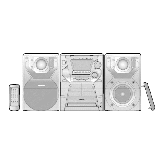
- Page 4 3. Turn on the power once again after one minute. Note: When the protection circuitry functions, the unit will not operate unless the power is first turned off and then on again. 3. Accessories Remote Control Transmitter FM indoor antenna (E,EB) FM indoor antenna (EG) AC mains lead (E,EG) AC mains lead (EB)
- Page 5 AM Loop antenna Antenna Plug Adaptor (EB) 4. Handling Precautions For Traverse Deck The laser diode in the traverse deck (optical pickup) may break down due to potential difference caused by static electricity of clothes or human body. So, be careful of electrostatic breakdown during repair of the traverse deck (optical pickup). - Handling of traverse deck (optical pickup) 1.
- Page 6 3. Take care not to apply excessive stress to the flexible board (FFC). 4. Do not turn the variable resistor (laser power adjustment). It has already been adjusted. - Grounding for electrostatic breakdown prevention 1. Human body grounding Use the anti-static wrist strap to discharge the static electricity from your body.
- Page 7 The traverse deck has a short point shorted with solder to protect the laser diode against electrostatics breakdown. Be sure to remove the solder from the short point before making connections. 5. Precaution of Laser Diode Caution : This product utilizes a laser diode with the unit turned "ON", invisible laser radiation is emitted from the pick up lens.
- Page 8 2. Den werkseitig justierten Einstellregler der Lasereinhit nicht verstellen. 3. Nicht mit optischen Instrumenten in die Fokussierlinse blicken. 4. Nicht über längere Zeit in die Fokussierlinse blicken. ADVARSEL: I dette a apparat anvendes laser. CAUTION! THIS PRODUCT UTILIZES A LASER. USE OF CONTROLS OR ADJUSTMENTS OR PERFORMANCE OF PROCEDURES OTHER THAN THOSE SPECIFIED HEREIN MAY RESULT IN HAZARDOUS RADIATION EXPOSURE.
- Page 9 6. Caution for AC Mains Lead...
- Page 10 7. Operation Procedures...
- Page 12 8. Disassembly and Main Component Replacement Procedures “ATTENTION SERVICER” Some chassis components may have sharp edges. Be careful when disassembling and servicing. 1. This section describes procedures for checking the operation of the major printed circuit boards and replacing the main components.
-
Page 13: Table Of Contents
2. For reassembly after operation checks or replacement, reverse the respective procedures. Special reassembly procedures are described only when required. 3. Select items from the following index when checks or replacement are required. Contents - Disassembly and assembly main unit 1. - Page 14 Step 2 Remove the top cabinet. Step 3 Remove the T-bracket.
- Page 15 Step 5 Turn locating pin on both sides 90°. (Locating pin need not to be bent back.) Step 6 Release the wires CN302, CN303, CN304, CN309 and CN502. Remove rear panel by pulling it backward and lift the rear panel assembly.
- Page 16 Step 7 Use a hexagonal wrench and turn clockwise to release the tray. Step 8 Pull the CD tray in the direction shown above.
- Page 17 Step 9 Remove the CD lid in the direction of the arrow. Step 11 Release the two catches shown above to remove the front cabinet from the CD traverse unit.
- Page 18 Step 12 Connect back the wire to CN302, CN303 and CN304. Use the extension wire (REXX0261) to connect to CN502. Use a FFC wire (REEX0137) to connect CN1 to CN309. 8.1.2. Checking for Panel, Main and Deck P.C.B.
-
Page 19: Checking Of The Power P.c.b
Step 1 Remove 2 screws each side. 8.1.3. Checking for Power P.C.B. -
Page 20: Main Component Replacement Procedures
8.2. Main Component Replacement Procedures 1. Replacement of the Traverse Deck Step 1 Follow the procedures in ‘Disassembly of the Traverse Unit’ ( Step 1 - Step 4 ) - Page 21 Step 3 Desolder the 4 legs of the 2 motors and pull out the Servo P.C.B. Step 4 Widen the 3 bosses with a flat screwdriver and pull out the 3 pins. Then remove the Traverse Deck. Step 5 Remove the flexible cable CN 701. - Removal of the flexible cable.
-
Page 22: Replacement Of The Power Amplifier Ic
Note: Insert a short pin into the flexible cable for traverse unit. - Installation of the CD servo P.C.B. after replacement Step 1 Connect the FFC board. Step 2 Install the CD servo P.C.B. in the traverse deck assembly. Note: Before installing the CD servo P.C.B., move the optical pickup towards the outer edge from the marking (black triangle). - Page 23 Step 2 Remove the wires at CN302, CN303 and CN304 and pull out the Main P.C.B. Step 3 Remove 4 screws fixed to the Power Amplifier IC. Step 4 Unsolder the terminals of Power Amp IC and replace the respective component.
-
Page 24: Disassembly And Assembly Of The Traverse Unit
8.3. Disassembly and assembly of the Traverse Unit Step 1 Push the lever from position A to B. Step 2 Pull the stopper (black) in the direction of arrow 1 and push the lever in the direction of arrow 2. Step 3 Push the stpeer (black) down until the white lever eject out. - Page 25 Step 1 Place the traverse unit as shown. Step 2 Press in the lever shaft in the direction of arrow 1 as shown and push the traverse unit into the position in the direction of arrow 2. Step 3 Pull the stopper in the direction of arrow 1 and release the lever in the direction of arrow 2 as shown.
-
Page 26: Disassembly And Assembly Of The Disc Tray
8.4. Disassembly and assembly of the Disc Tray Step 2 With lifting the claw in the direction of arrow 1, draw the clamp SW P.C.B. in the direction of arrow 2. Step 3 Remove the mechanism cover. Step 4 Insert the gear with hexagonal wrench into the hole. - Page 27 Step 5 Rotate the hexagonal wrench in the direction of arrow (clockwise), and then open the disc tray fully. Step 6 Upset the CD changer unit again. Step 7 Release both the claws, and then draw the disc tray. Step 8 With forcing the left guide bar manually because the left guide bar interfers with claw, draw the disc tray.
- Page 28 Step 1 Slide the drive rack fully in the direction of arrow. Step 2 Holding the drive rack not to move, install the disc tray.
- Page 29 Step 3 Align the drive rack with the driver gear. Step 4 Holding the disc tray manually, rotate the pulley gear in the direction of arrow. Step 5 Rotate the gear 5 or 6 times manually, and then push the disc tray. 9.
- Page 30 9.3. Cassette Mechanism Test (For error code H01, H02, H03, F01, F02) 1. Press “TAPE, DECK 1/2” to select Deck 2. 2. Load a cassette tape with the erasure prevention tab, remove from left side only and close the cassette holder. 3.
- Page 31 7. Press “PLAY/TUNE/TIME ADJ UP” (After TPS function, tape will stop automatically) 8. Press “REC/STOP” (Tape will not move) 9. Press “STOP/TUNE MODE” to indicate Error code. - If several problem exist, error code will change each time when “ /TUNE MODE”...
- Page 32 10. Description of Error Code 10.1. Error detection for Cassette Mechanism block Error Error Problem condition Display MODE SW Faulty operation of cassette mechanism. detection error Faulty contact or short-circuit of mechanism mode switch (S951, S971). REC INH SW Recording not possible. detection error Faulty contact or short-circuit of REC INH switch (S974, S975).
- Page 33 10.3. Power Supply related error detection Error Error Problem condition Display POWER AMP When POWER is switched on, power become off automatically. output abnormal During normal operation, if DC DET become L, PCNT shall become L and the error display on the left shall be displayed. (IC501) 11.
- Page 34 adjustment result. FLOCK, TLOCK and CLVS status shall be shown as below: During the above display, executing CD PLAY will display auto adjustment result for CD PLAY mode. 12. Measurements and Adjustments 12.1. Cassette Deck Section - Measurement Condition - Tape edit: NORMAL - Record timer: OFF - Make sure head, capstan and press roller are clean.
- Page 35 12.1.2. Bias and Erase Voltage Check 1. Set the unit “AUX” position. 2. Insert the Normal blank tape (QZZCRA) into DECK 2 and the unit to “REC” mode (use “ REC/STOP” key). 3. Measure and make sure that the output is within the standard value.
- Page 36 12.2. Tuner Section 12.2.1. AM-IF Alignment SIGNAL GENERATOR OR RADIO DIAL INDICATOR REMARKS ADJUSTMENT SWEEP GENERATOR SETTING (ELECTRONIC (Shown in VOLTMETER CONNECTIONS FREQUENCY Fig.3) OSCILLOSCOPE) Fashion a 450 kHz 30% Point of non- Headphones Jack Z102 (AM Adjust for maximum loop of Mod.
- Page 37 12.3. Alignment Points Cassette Deck section Tuner section...
- Page 38 13. Illustration of IC’s, Transistors and Diodes 14. Terminal Function of IC’s 14.1. IC701 (AN8885SBE1) Servo Amplifier Pin No. Mark Function Tracking signal input 1 Tracking signal input 2 Power supply Focus signal input terminal 1 Focus signal input terminal 2 APC amp input APC amp output RFsumming output...
- Page 41 OPTICAL PICKUP IC701 AN8885SBE1 SERVO AMP SEMICONDUCTOR LASER OFTR TENV DET. Q701 LASER OFTR POWER DRIVE OFTR DET. LDON /RFDET /RFDET DET. PHOTO DETECTOR FEOUT VCBA Subtracter VREF Subtracter VCBA N.C. TRACKING FOCUS COIL COIL SYNDROME DIGITAL AUDIO INTERFACE CALCULATION PHASE FREQUENCY COMPARATOR...
- Page 42 AM ANT FM ANT Z101 Z120 (FM) CF202 CF201 Q101 COIL COIL MIXER IF AMP RF AMP BUFFER Q110 SWITCH (FM) DECODER RM AMP BUFFER PHASE PILOT CANCEL STEREO LEVEL S-CURVE SWITCH AM/FM COMP BUFFER TUNING DRIVE PILOT Z102 IC101 X102 LA1833NMNTLM FM/AM IF AMP,...
- Page 43 TA7291P MOTOR DRIVE Vs 8 OUT1 OUT2 Q350 SWITCH (PLUNGER SUPPLY) POWER SUPPLY CONTROL Q604 STATUS SWITCH Q351 Q605 SWITCH SUBQ (PLUNGER SWITCH SUPPLY) D614 ST/DO Q606 BLKCK SWITCH /CDRST RESTSW D619 CE/MLD MLD/PLLCE IC600 DI/MDATA MDATA/PLLDA M38B79MFA158 MICROPROCESSOR CL/MCLK MCLK/PLLCLK X600 SW600...
- Page 44 IC1001 AN7348STA-E1 P.B. EQ /TPS AMP Q1012(Q1013) REC AMP/ALC IC1003 MUTING 24(23) BA4558FE2 (DECK 1) 1(2) P.B. HEAD 20(5) BUFFER 22(3) Q1014 (Q1015) 21(4) Q1024 (DECK 2) BUFFER R/P HEAD DRIVE 17(8) 18(7) Q1020 LOGIC L/H (Q1021) FILTER NOR/CrO & HI/LO LOGIC Q1016 LOGIC...
- Page 45 FILTER FILTER H_OUT_L(R) (10) (13) (14) IC302 M5218AP Q400(Q200) (31) BUFFER MUTING OUTL(R) 45(46) INLC(R) HP_L(R) 51(52) RECL(R) 43(44) IC301 INLB(R) BH3874AKS2 AUDIO SOUND PROCESSOR 47(48) INLD(R) JK305 Q450 (Q250) MUTING FROM CD UNIT SWITCH 41(42) CD SIGNAL INLA(R) H_OUT_L(R) Q306 AUDIO MUTING...
- Page 46 SIGNAL LINES MAIN SIGNAL LINE CD SIGNAL LINE AM SIGNAL LINE PLAYBACK SIGNAL LINE FM OSC SIGNAL LINE AM OSC SIGNAL LINE FM & AM SIGNALS LINE RECORDING SIGNAL LINE FM SIGNAL LINE ) indicates Pin No. of right channel IC500 RSN3502C POWER IC...
- Page 57 SCHEMATIC DIAGRAM -1 : +B SIGNAL LINE : CD SIGNAL LINE CD SERVO CIRCUIT R701 OPTICAL PICKUP CIRCUIT Q701 C701 2SA1037AKSTX 6.3V33 3.2V C703 LASER POWER DRIVE LASER DIODE 6.3V100 Q701 CN701 2.7V ((2.3V)) 0.9V ((2V)) C704 R750 LD GND NBOUT C707 C714...
- Page 58 SCHEMATIC DIAGRAM - 2 : +B SIGNAL LINE : CD SIGNAL LINE CD SERVO CIRCUIT R717 C727 50V1 C725 1000P R721 C726 1000P R718 C728 50V1 C731 6.3V220 CN702 C730 LCH OUT C732 C733 6.3V220 A.GND C754 470P RCH OUT C753 470P +3.3V...
- Page 59 SCHEMATIC DIAGRAM - 3 : +B SIGNAL LINE : FM SIGNAL LINE : AM SIGNAL LINE : FM OSC SIGNAL LINE : AM OSC SIGNAL LINE : FM/AM SIGNAL LINE MAIN/TUNER CIRCUIT Q106 Q101 Q106 KRA102MTA 2SC2058SPTA R104 POWER SUPPLY CONTROL FM IF AMP (0V) TUNER PACK Z120 (EN17290G1Y)
- Page 60 SCHEMATIC DIAGRAM - 4 : +B SIGNAL LINE : MAIN SIGNAL LINE : FM/AM SIGNAL LINE : RECORD SIGNAL LINE : CD SIGNAL LINE PANEL CIRCUIT (CP605) ON SCHEMATIC DIAGRAM-8 MAIN CIRCUIT CN303 20 19 18 17 16 15 14 13 12 11 10 28 27 26 25 R211 R212...
- Page 61 SCHEMATIC DIAGRAM - 5 : -B SIGNAL LINE : +B SIGNAL LINE : MAIN SIGNAL LINE PANEL CIRCUIT (CP607) ON SCHEMATIC MAIN CIRCUIT DIAGRAM-8 CN302 24 23 22 21 20 19 18 17 16 15 14 13 12 11 10 C375 1000P C228...
- Page 62 SCHEMATIC DIAGRAM - 6 : +B SIGNAL LINE : -B SIGNAL LINE : MAIN SIGNAL LINE MAIN CIRCUIT (-29.86V)<-29.85V> (-44.1V)<-43.8V> -29.89V((-29.84V)) -43.9V((-42.9V)) RL1N4003S-P [-29.94V] [-44.2V] R332 D313 Q308 C359 R331 (-30.45V) 2SB621ARSTA 4.7K 0.01 <-30.48V> C360 -30.5V REGULATOR 63V100 ((-30.44V)) FOR FL DISPLAY [-30.55V] CN301...
- Page 63 SCHEMATIC DIAGRAM - 7 : +B SIGNAL LINE : MAIN SIGNAL LINE PANEL CIRCUIT FL600 RSL0314-F C600 35V22 TACT SWITCH (1) CIRCUIT Z940 RCDGP1U26XV REMOTE CONTROL SENSOR C941 0.01 D949 C940 SLR325DCT31 1000P Q600 (9.21V)<9.22V> (9.21V)<9.21V> R949 9.21V((9.16V)) 9.2V((9.15V)) D949 [9.23V] R624 [9.21V]...
- Page 64 SCHEMATIC DIAGRAM - 8 : +B SIGNAL LINE : MAIN SIGNAL LINE DECK CIRCUIT (CN1001) ON : -B SIGNAL LINE : CD SIGNAL LINE SCHEMATIC DIAGRAM-10 PANEL CIRCUIT H600/W600 Q603 2SA933SSTA SWITCH DECK +6V SUPPLY C634 R651 R652 35V22 D613 L605 MA4020LTA RLQB101JTD-D...
- Page 65 SCHEMATIC DIAGRAM - 9 : +B SIGNAL LINE : PLAYBACK SIGNAL LINE : -B SIGNAL LINE : RECORD SIGNAL LINE DECK CIRCUIT R1055 2.2K C1038 R1098 220P R1017 8.2K CS1001 R1095 100K R1032 R1015 HEAD C1015 C1012 C1034 1000P 1000P R1039 50V3.3 C1019...
- Page 66 SCHEMATIC DIAGRAM - 10 : +B SIGNAL LINE : -B SIGNAL LINE : PLAYBACK SIGNAL LINE : RECORD SIGNAL LINE MAIN CIRCUIT (CN304) ON SCHEMATIC DIAGRAM-4 DECK CIRCUIT H1001/W1001 10 9 R1072 R1077 R1074 C1057 C1058 C1060 50V3.3 R1069 4700P 6.8K C1054 R1067...
- Page 67 SCHEMATIC DIAGRAM - 11 : +B SIGNAL LINE : -B SIGNAL LINE : MAIN SIGNAL LINE POWER CIRCUIT IC500 IC500 RSN3502C-P POWER IC C557 C558 0.047 0.047 Q514-Q515 R539 C539 R525 C537 KTC3199GRTA 1000P 6.3V220 330K AGC CONTROL SWITCH R538 R542 C520 JK501...
- Page 68 SCHEMATIC DIAGRAM -12 : +B SIGNAL LINE TRANSFORMER CIRCUIT D575 R584 R583 R582 D574 1T3T 1T3T D576 D570 (5.92V) <5.96V> 5.96V ((5.94V))[5.97V] 1T3T 1T3T (9.19V) <9.06V> R580 Q570 C573 8.86V ((8.22V)) [9.27V] 0.01 C572 (6.58V) <6.58V> 0.01 6.59V ((6.58V)) [6.6V] R581 D577 D571...
- Page 69 Pin No. Mark Function BCLK N.C. LRCK N.C. SRDATA O N.C. DVDD1 Power supply input (for digital circuit) DVSS1 GND (for digital circuit) Digital audio interface signal output (Latches data at first transition) MCLK Microprocessor command clock signal input MDATA Microprocessor command data signal input...
- Page 70 Pin No. Mark Function SMCK 1/2-diveded clock signal of crystal osscillating at MSEL = “H” (fSMCK = 8.4672 MHz) 1/4-divided clock signal of crystal oscillating at MSEL = “L” (fSMCK = 4.2336 MHz) CSEL Frequency Selection Terminal H = 33.8688 MHz ;...
- Page 71 Pin No. Mark Function Off-track signal input ("H" : off track) TRCRS Track cross signal input /RFDET RF detection signal input ("L" : detection) Dropout signal input ("H" : Dropout) LDON Laser on signal output ("H" : ON) PLLF2 N.C. DSLF2 Tracking Offset alignment output/...
- Page 72 Pin No. Mark Function X1 IN Crystal oscillating circuit input (f = 16.9344MHz) X2 OUT Crystal oscillating circuit input (f = 16.9344 MHz) Power supply input (for oscillating circuit) BYTCK Byte clock output /CLDCK - Sub-code frame clock signal output (fCLDCK = 7.35 kHz during normal playback)
- Page 73 Pin No. Mark Function RSEL RF signal polarity assignment input (at "H" level, RSEL="H", at "L" level, RESL= "L") IOVDD 5V supply input PSEL Test terminal (connected to Gnd) MSEL SMCK oscillating frequency designation input (“L” :4.2336 MHz, “H”: 8.4672 MHz) SSEL SUBQ output mode select (“H”:Q-code...
- Page 74 Pin No. Mark Function /RST RESET output terminal N.C. Motor Drive (2) input Turntable motor drive signal (“L :ON) N.C. Motor driver (1) input N.C. PVCC1 I Power supply (1) for driver PGND1 - Ground connection (1) for driver N.C. Motor driver (1) reverse- action output Motor driver (1) forward-...
- Page 75 Pin No. Mark Function DECK2 Tape mecha condition input (Half2 /Reci_F/Mode/Reci_R) KEY3 Key 3 input KEY2 Key 2 input KEY1 Key 1 input V_JOG_AD I Volume jog A-D detection input J_JOG_AD I EQ Joy jog A-D detection input CHG_AD1 I (Open Clamp) Chngr sw A-D detection input 1...
- Page 76 Pin No. Mark Function CD command data MDATA/ output/ tuner PLL PLLDA data output Remote control input BLKCK CD block clock input (INV) MLD/ CD command load PLLCE output/ tuner PLL chip enable SYNC AC failure detect input DCDET 1 I DC detect input 1 DCDET 2 I DC detect input 2...
- Page 77 Pin No. Mark Function REG_IN Region and function EE_CS setting input and eeprom chip select output ECONO Main transormer control output for economy mode RESTSW I CD limit SW input for the most inner point (Active Low) SER4 EEPROM_CLK / EXP2_CLK/MK_CLK SER3 ASP latch...
- Page 78 : CD 2 switch S903 : CD 3 switch S904 : CD 4 switch S905 : CD 5 switch S906 : Rec/Stop select switch S907 : Rec Mode select switch S908 : Tape Edit select switch S909 : Tune Down switch S910 : FM Mode/BP switch S911...
- Page 79 : CD switch S945 : Super Sound EQ switch S950 : Deck 2 switch S951 : Mode switch S952 : Half switch S953 : Cr02 switch S956 : Power switch S958 : Play/Rec Timer switch S959 : Clock/Timer switch S960 : RDS switch S961 : Display/Demo switch...
- Page 80 : RECINH_F switch : Push switch : Push switch : Leaf switch : CD switch : Lock switch SW600 : Joy Jog switch VR900 : VR Volume Jog - The voltage value and waveforms are the reference voltage of this unit measured by DC electronic voltmeter (high impedance) and oscilloscope on the basis of chassis.
- Page 81 - Put a conductive mat on the work table. - Ground the soldering iron. - Do not touch the pins of IC, LSI or VLSI with fingers directly. “CAUTION: REPLACE FUSIBLE RESISTOR WITH THE SAME TYPE RSFMB40KT-L FUSIBLE RESISTOR”“ATTENTION: REMPLACER LA RESISTANCE FUSIBLE PAR UNE RESISTENCE FUSIBLE DE MEME TYPE RSFMB40KT-L.
- Page 82 19. Troubleshooting Guide...
- Page 83 20. Parts Location and Replacement Parts List Notes:...
- Page 84 - Important safety notice: Components identified by mark have special characteristics important for safety. Furthermore, special parts which have purposes of fire-retardent (resistors), high-quality sound (capacitors), low noise (resistors), etc are used. When replacing any of these components, be sure to use only manufacturer’s specified parts shown in the parts list.
- Page 85 Ar : Arabic Du : Dutch It : Italian Sp : Spanish Cf : Canadian French En : English Ko : Korean Sw : Swedish Cz : Czech Fr : French Po : Polish Co : Traditional Chinese Da : Danish Ge : German...
- Page 86 20.1.2. Deck Mechanism Parts List...
- Page 87 Ref. No. Part No. Part Name & Description Remarks CASSETTE DECK RED0067 HEAD BLOCK UNIT RED0068 R/P HEAD BLOCK UNIT RDG0300 REEL BASE GEAR RDG0301 WINDING RELAY GEAR RDK0026 MAIN GEAR RDR0029 RELAY PULLEY RDV0033-4 WINDING BELT RDV0064 CAPSTAN BELT RDV0057 MAIN BELT B RMB0312...
- Page 89 20.2.2. CD Loading Mechanism Parts List...
- Page 90 Ref. No. Part No. Part Name & Description Remarks TRAVERSE DECK RML0517 TIMING LEVER RML0516 PLUNGER LEVER RMB0551 UPPER SPINDLE SPRING RMQ0744 LOWER HOOK RDV0056 BELT RML0525 FRONT LOCK LEVER RML0526 DISC LEVER RDG0424 DRIVE GEAR RDG0425 CHANGE GEAR RDG0427 TRAVERSE CAM GEAR RDG0428 TRAVERSE RELAY GEAR...
- Page 91 Ref. No. Part No. Part Name & Description Remarks RDG0431 RELAY GEAR ‘B’ RME0262 DISK LEVER SP. RMA1105 SUPPORT PLATE RAE0152Z-3 TRAVERSE 358-1 SHGD113-1 FLOATING CUSHION 358-2 SNSD38 TRV MOTOR ASSY SCREW 358-3 RAF0150A-4S 50A OPTICAL PICKUP 358-4 RDG0247 DRIVE GEAR 358-5 RDG0248 RELAY GEAR...
- Page 94 20.3.2. Cabinet Parts List...
- Page 95 Ref. No. Part No. Part Name & Description Remarks CABINET AND CHASSIS REEX0129 14P FFC REEX0101 28P FFC REEX0127 20P FFC REEX0130 19P FFC RGB0113-N PANA BADGE RGKX0070-S CD LID RGKX0071-AB CD ORNAMENT [MAVD] RGLX0028-Q POWER LIGHTING CHIP RGLX0030-Q DISC LIGHT CHIP RGPX0038E-SL FRONT PANEL [MAVD] RGRX0017G-AB REAR PANEL...
- Page 96 Ref. No. Part No. Part Name & Description Remarks XTW3+15T SCREW XTW3+8T SCREW RKWX0156 FL FILTER RMC0158-S TR FIXTURE RGUX0380Z-S RDS BUTTON [MAVD] REXX0259 8P WIRE 20.4. Component Parts List Ref. No. Part No. Part Name & Description Remarks PRINTED CIRCUIT BOARDS REPX0192D CD SERVO P.C.B.
- Page 97 Ref. No. Part No. Part Name & Description Remarks RVTDTC143EST TRANSISTOR Q101 2SC2058SPTA TRANSISTOR Q106 KRA102MTA TRANSISTOR Q110 2SC3311ARTA TRANSISTOR Q200 KTD1304TA TRANSISTOR Q250 KTD1304TA TRANSISTOR Q306 KRA102STA TRANSISTOR Q307 KRC111STA TRANSISTOR Q308 2SB621ARSTA TRANSISTOR Q350 2SB621ARSTA TRANSISTOR Q351 KRC102STA TRANSISTOR Q400 KTD1304TA...
- Page 98 Ref. No. Part No. Part Name & Description Remarks Q1009 KTC3875GRTA TRANSISTOR Q1010 KTC3875GRTA TRANSISTOR Q1011 KTC3875GRTA TRANSISTOR Q1012 KTD1304TA TRANSISTOR Q1013 KTD1304TA TRANSISTOR Q1014 2SC2412KT96R TRANSISTOR Q1015 2SC2412KT96R TRANSISTOR Q1016 KRA102STA TRANSISTOR Q1017 KTD1146YTA TRANSISTOR Q1018 KTA12710YTA TRANSISTOR Q1019 KTA12710YTA TRANSISTOR Q1020...
- Page 99 Ref. No. Part No. Part Name & Description Remarks D529 RVD1SS133TA DIODE D530 RVD1SS133TA DIODE D570 1T3T DIODE D571 1T3T DIODE D572 MTZJ6R8BTA DIODE D573 RVD1SS133TA DIODE D574 1T3T DIODE D575 1T3T DIODE D576 1T3T DIODE D577 1T3T DIODE D605 SLI325URCT31 DIODE D610...
- Page 100 Ref. No. Part No. Part Name & Description Remarks S907 EVQ21405R SW REC MODE S908 EVQ21405R SW TAPE EDIT S909 EVQ21405R SW TUNE DOWN S910 EVQ21405R SW FM MODE/BP S911 EVQ21405R SW MEMORY S912 EVQ21405R SW TUNE MODE S913 EVQ21405R SW TUNE UP S920 EVQ21405R...
- Page 101 Ref. No. Part No. Part Name & Description Remarks CP500 RJT057G12 12P P2 MQ CONNECTOR CP501 RJT057G12 12P P2 MQ CONNECTOR CP605 RJS1A9420 20P FFC CONNECTOR CP606 RJS1A6219-1 19P FFC CONNECTOR CP607 RJS1A9428-1 28P FFC CONNECTOR CP900 RJU066H12M 12P BTB CONNECTOR CP1001 RJT071K09A 9P B/B CONNECTOR...
- Page 102 Ref. No. Part No. Part Name & Description Remarks OSCILLATORS X102 RLFDFT22DD DISCRIMINATOR X103 RSXC7M20S05T CRYSTAL OSCILLATOR X600 RSXZ4M19D01T CRYSTAL OSCILLATOR X601 RSXD32K7S02 CRYSTAL OSCILLATOR X701 RSXZ16M9M08T CERAMIC OSCILLATOR X990 RSXC4M33S02T CERAMIC OSCILLATOR DISPLAY TUBE FL600 RSL0314-F FUSES XBA2C16TB0 1.6A PRIMAY FUSE FUSE HOLDERS EYF52BC FUSE HOLDER...
- Page 103 Ref. No. Part No. Part Name & Description Remarks W500B REXX0202 2P STANDBY WIRE W600 RWJ0208155RX 8P PANEL TO DECK W601 REXX0253 6P WIRE W920 RWJ0206250XX 6P (2) FLAT WIRE W940 RWJ1109140RR 9P WIRE W1001 RWJ8010160RX 10P WIRE W1002 RWJ0102065CK WIRE RESISTORS ERDS2TJ102T...
- Page 104 Ref. No. Part No. Part Name & Description Remarks R152 ERJ3GEY0R00V 0 1/16W R201 ERJ3GEYJ272V 2.7K 1/16W R202 ERJ3GEYJ103V 10K 1/16W R207 ERJ3GEYJ152V 1.5K 1/16W R208 ERJ3GEYJ103V 10K 1/16W R209 ERJ3GEYJ473V 47K 1/16W R210 ERJ3GEYJ102V 1K 1/16W R211 ERJ3GEYJ222V 2.2K 1/16W R212 ERJ3GEYJ472V 4.7K 1/16W...
- Page 105 Ref. No. Part No. Part Name & Description Remarks R374 ERJ3GEYJ153V 15K 1/16W R375 ERJ3GEYJ153V 15K 1/16W R378 ERJ3GEYJ273V 27K 1/16W R379 ERJ3GEYJ472V 4.7K 1/16W R380 ERDS1FVJ470T 47 1/2W R381 ERJ3GEYJ473V 47K 1/16W R382 ERJ3GEYJ473V 47K 1/16W R384 ERJ3GEYJ473V 47K 1/16W R385 ERJ3GEYJ473V 47K 1/16W...
- Page 106 Ref. No. Part No. Part Name & Description Remarks R520 ERD25FVJ4R7T 4.7 1/4W R522 ERDS2TJ562T 5.6K 1/4W R523 ERDS2TJ683T 68K 1/4W R524 RSFMB10KT-L FUSE PROTECTOR R525 ERDS2TJ334T 330K 1/4W R526 ERDS2TJ223T 22K 1/4W R527 ERDS2TJ2R2T 2.2 1/4W R528 ERDS2TJ2R2T 2.2 1/4W R529 ERDS2TJ2R2T 2.2 1/4W...
- Page 107 Ref. No. Part No. Part Name & Description Remarks R602 ERDS2TJ472T 4.7K 1/4W R605 ERDS2TJ392T 3.9K 1/4W R611 ERDS2TJ104T 100K 1/4W R612 ERDS2TJ104T 100K 1/4W R613 ERDS2TJ104T 100K 1/4W R614 ERDS2TJ104T 100K 1/4W R615 ERDS2TJ104T 100K 1/4W R616 ERDS2TJ104T 100K 1/4W R617 ERDS2TJ104T 100K 1/4W...
- Page 108 Ref. No. Part No. Part Name & Description Remarks R664 ERDS2TJ101T 100 1/4W R665 ERDS2TJ101T 100 1/4W R666 ERDS2TJ101T 100 1/4W R667 ERDS2TJ562T 5.6K 1/4W R668 ERDS2TJ562T 5.6K 1/4W R669 ERDS2TJ562T 5.6K 1/4W R670 ERDS2TJ104T 100K 1/4W R671 ERDS2TJ104T 100K 1/4W R672 ERDS2TJ104T 100K 1/4W...
- Page 109 Ref. No. Part No. Part Name & Description Remarks R735 ERJ6GEYJ101V 100 1/10W R736 ERJ3GEYJ101V 100 1/16W R741 ERJ3GEYJ473V 47K 1/16W R742 ERJ6GEYJ224V 220K 1/10W R744 ERJ3GEYJ124V 120K 1/16W R749 ERJ3GEYJ472V 4.7K 1/16W R750 ERJ6GEYJ4R7V 4.7 1/10W R753 ERJ3GEYJ100V 10 1/16W R900 ERDS2TJ223T 22K 1/4W...
- Page 110 Ref. No. Part No. Part Name & Description Remarks R992 ERDS2TJ102T 1K 1/4W R993 ERDS2TJ102T 1K 1/4W R994 ERDS2TJ121T 120 1/4W R995 ERDS2TJ102T 1K 1/4W R996 ERDS2TJ103T 10K 1/4W R998 ERDS2TJ122T 1.2K 1/4W R999 ERDS2TJ102T 1K 1/4W R1001 ERJ3GEYJ1R0V 1 1/16W R1003 ERJ3GEYJ103V 10K 1/16W...
- Page 111 Ref. No. Part No. Part Name & Description Remarks R1059 ERJ3GEYJ103V 10K 1/16W R1060 ERJ3GEYJ391V 390 1/16W R1061 ERJ3GEYJ2R7V 2.7 1/16W R1062 ERJ3GEYJ2R7V 2.7 1/16W R1063 ERJ3GEYJ102V 1K 1/16W R1064 ERJ3GEYJ102V 1K 1/16W R1065 ERJ3GEYJ102V 1K 1/16W R1066 ERJ3GEYJ102V 1K 1/16W R1067 ERJ3GEYJ153V 15K 1/16W...
- Page 112 Ref. No. Part No. Part Name & Description Remarks C111 ECEA1HKA4R7B 4.7 50V C112 ECUV1E103KBV 0.01 25V C113 ECUV1H102KBV 1000P 50V C114 ECEA1HKA3R3B 3.3 50V C115 ECEA1HKA4R7B 4.7 50V C116 ECUV1C333KBV 0.033 16V C117 ECUV1E103KBV 0.01 25V C118 ECUV1E103KBV 0.01 25V C119 ECQP2A681JZT 680P 100V...
- Page 113 Ref. No. Part No. Part Name & Description Remarks C301 ECUV1H102KBV 1000P 50V C303 ECEA1CKA100B 10 16V C304 ECUV1C473KBV 0.047 16V C305 ECUV1H472KBV 4700P 50V C306 ECEA1HKAR33B 0.33 50V C307 ECEA1HKAR33B 0.33 50V C308 ECUV1C104KBV 0.1 16V C310 ECUV1C473KBV 0.047 16V C311 ECEA1HKAR33B 0.33 50V...
- Page 114 Ref. No. Part No. Part Name & Description Remarks C404 ECUV1H221KBV 220P 50V C407 ECEA1CKA100B 10 16V C425 ECEA1HKA3R3B 3.3 50V C426 ECUV1C683KBV 0.068 16V C427 ECUV1H681KBV 680P 50V C428 ECEA1CKA100B 10 16V C429 ECUV1H101KCV 100P 50V C430 ECUV1H470JCV 47P 50V C431 ECEA1CKA100B 10 16V...
- Page 115 Ref. No. Part No. Part Name & Description Remarks C558 ECBT1H473KB5 0.047 50V C570 RCEA1C102B-S 1000P 16V C572 ECKR1H103ZF5 0.01 50V C573 ECKR1H103ZF5 0.01 50V C574 ECEA1EKA470B 47 25V C575 ECKR1H103ZF5 0.01 50V C576 ECEA1VKA4R7B 4.7 35V C600 ECEA1VKA220B 22 35V C606 ECBT1H101KB5 100P 50V...
- Page 116 Ref. No. Part No. Part Name & Description Remarks C699 ECBT1E104ZF5 0.1 25V C701 ECEA0JKA330I 33 6.3V C702 ECUV1C104KBV 0.1 16V C703 ECEA0JKA101I 100 6.3V C704 ECUV1C104KBV 0.1 16V C706 ECUV1H272KBV 2700P 50V C707 ECUV1E273KBV 0.027 25V C710 ECUV1H121KCV 120P 50V C711 ECUV1C104ZFV 0.1 16V...
- Page 117 Ref. No. Part No. Part Name & Description Remarks C993 ECBT1H470J5 47P 50V C994 ECBT1H470J5 47P 50V C995 ECEA1HKA100B 10 50V C996 ECBT1H331KB5 330P 50V C997 ECEA1HKA100B 10 50V C998 ECBT1H561KB5 560P 50V C1001 ECUV1H103ZFV 0.01 50V C1002 ECEA1HKN2R2B 2.2 50V C1003 ECQP1152JZT 1500P 100V...
- Page 118 Ref. No. Part No. Part Name & Description Remarks C1055 ECEA1HKA0R1B 0.1 50V C1056 ECUV1H103KBV 0.01 50V C1057 ECEA1HKA3R3B 3.3 50V C1058 ECUV1H470JCV 47P 50V C1059 ECUV1H101KCV 100P 50V C1060 ECUV1H472KBV 4700P 50V C1061 ECUV1H101KCV 100P 50V C1062 ECUV1C104ZFV 0.1 16V C1063 ECUV1C104ZFV 0.1 16V...
- Page 119 Ref. No. Part No. Part Name & Description Remarks PACKING MATERIALS RPGX0759 PACKING CASE [MAVD] RPNX0123 POLYFOAM [MAVD] RPFX0007 MIRAMAT BAG ACCESSORIES N2QAGB000006 REMOTE CONTROLLER [MAVD] A1-1 R0280-720010 R/C BATTERY COVER [MAVD] RJA0043-1C AC CORD EG E RJA0044-3C AC CORD RQT5662-E O/I BOOK (Sp) RQT5663-R...
Need help?
Do you have a question about the SA-AK22 and is the answer not in the manual?
Questions and answers