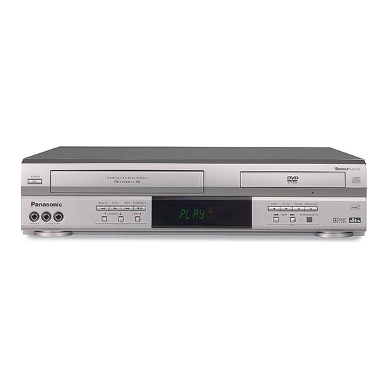
Panasonic PV-D4733S-K Service Manual
Dvd/vcr deck
Hide thumbs
Also See for PV-D4733S-K:
- Operating instructions manual (120 pages) ,
- Operating instructions manual (60 pages)

Related Manuals for Panasonic PV-D4733S-K


Summary of Contents for Panasonic PV-D4733S-K
- Page 1 ORDER NO. MKE0304802A1 DVD/VCR DECK PV-D4733S-K / PV-D4753S-K / PV-D4763S-K Please file and use this manual together with the service manual for Model No. PV-D4743S-K, Order No. MKE0301800C1. SPECIFICATIONS...
-
Page 2: Comparison Chart
1. DIFFERENCES BETWEEN PV-D4733S-K and PV- D4743S-K 1.1. COMPARISON CHART 1.1.1. MECHANICAL REPLACEMENT PARTS LIST... - Page 3 1.1.2. ELECTRICAL REPLACEMENT PARTS LIST 2. DIFFERENCES BETWEEN PV-D4753S-K and PV- D4743S-K 2.1. COMPARISON CHART 2.1.1. MECHANICAL REPLACEMENT PARTS LIST 2.1.2. ELECTRICAL REPLACEMENT PARTS LIST 3. DIFFERENCES BETWEEN PV-D4763S-K and PV- D4743S-K 3.1. COMPARISON CHART 3.1.1. MECHANICAL REPLACEMENT PARTS LIST...
-
Page 4: Exploded View
3.1.2. ELECTRICAL REPLACEMENT PARTS LIST 4. EXPLODED VIEW 4.1. CHASSIS FRAME AND CASING PARTS SECTION... -
Page 5: Replacement Parts List
5. REPLACEMENT PARTS LIST BEFORE REPLACING PARTS, READ THE FOLLOWING: 5.1. REPLACEMENT NOTES 5.1.1. General Notes 1. Use only original replacement parts: To maintain original function and reliability of repaired units, use... -
Page 6: Important Safety Notice
only original replacement parts which are listed with their part numbers in the parts list. 2. IMPORTANT SAFETY NOTICE Components identified by the sign have special characteristics important for safety. When replacing any of these components, use only the specified parts. 3. - Page 7 Non Repairable Board Ass'y MGF CHIP: Metal Glaze Film Chip C CHIP: Ceramic Chip COMPLX CMP: Complex Component W FLMPRF: Wirewound Flameproof C.B.A.: Circuit Board Assembly P.C.B.: Printed Circuit Board E.S.D.: Electrostatically Sensitive Devices 3. When replacing 0 resistor, a wire can be substituted for it. 4.
-
Page 8: Electrical Replacement Parts List
5.2. ELECTRICAL REPLACEMENT PARTS LIST Definition of Parts supplier: 1. All parts are supplied from MKI. PRINTED CIRCUIT BOARD ASSEMBLY Ref. No. Part No. Part Name & Description Remarks LSEP2095HE MAIN C.B.A. ( C ) E.S.D. RTL LSEP2095HD MAIN C.B.A. ( E ) E.S.D. - Page 9 Ref. No. Part No. Part Name & Description Remarks IC1001 CNC1S101RLL1 IC, LINEAR IC1002 C0DAEMZ00005 IC, LINEAR IC1002 C0DAEMZ00001 IC, LINEAR IC1002 C0DAEMZ00005 IC, LINEAR IC1501 C5HABZZ00101 IC, LINEAR IC1502 CNC1S101RLL1 IC, LINEAR IC1503 C0DAEMZ00005 IC, LINEAR IC1503 B1AZKD000001 IC, LINEAR IC1503 C0DAEMZ00001 IC, LINEAR IC3001...
- Page 10 Ref. No. Part No. Part Name & Description Remarks Q1001 2SC4953001KT TRANSISTOR SI NPN Q1001 B1BADP000012 TRANSISTOR SI NPN Q1001 2SC4533003KT TRANSISTOR SI NPN Q1001 2SC5842001KT TRANSISTOR SI NPN Q1002 2SD225900A TRANSISTOR SI NPN Q1051 B1BACC000010 TRANSISTOR SI NPN Q1051 2SD1581-T TRANSISTOR SI NPN Q1052...
- Page 11 Q4011 UNR521500L TRANSISTOR SI NPN CHIP Ref. No. Part No. Part Name & Description Remarks Q4011 B1GBCFJA0006 TRANSISTOR SI NPN CHIP Q4012 UNR511500L TRANSISTOR SI PNP CHIP Q4012 B1GDCFJJ0025 TRANSISTOR SI PNP CHIP Q4101 2SD0601ARL TRANSISTOR SI NPN CHIP Q4304 UNR221200L TRANSISTOR SI NPN CHIP Q4304...
- Page 12 Ref. No. Part No. Part Name & Description Remarks D1009 SFPJ-53 DIODE SI D1010 ERZV10V361CS SUEGE ABSORBER D1010 D4EAA3610001 SURGE ABSORBER D1011 B0AAKT000010 DIODE SI D1011 B0EAKT000027 DIODE SI D1011 B0EAKT000030 DIODE SI D1012 B0AAKT000010 DIODE SI D1012 B0EAKT000027 DIODE SI D1012 B0EAKT000030 DIODE SI D1013...
- Page 13 Ref. No. Part No. Part Name & Description Remarks D1508 RGP15GL-5008 DIODE SI D1509 B0JAPG000024 DIODE SI D1509 B0JAPG000020 DIODE SI D1509 B0JAPG000021 DIODE SI D1517 MAZ4056NMF DIODE ZENER 5.6V D1522 B0AAML000001 DIODE SI D1522 B0EAKL000008 DIODE SI D1525 MAZ4047NMF DIODE ZENER 4.7V D1527 B0AAML000001 DIODE SI...
- Page 14 Ref. No. Part No. Part Name & Description Remarks R1001 VRESC2TK275 CARBON 1/2W 2.7M R1001 VRESC2TK275C CARBON 1/2W 2.7M R1001 VRESC2TK275T CARBON 1/2W 2.7M R1003 D0AF334JA038 CARBON 1/2W 330K R1004 ERG2SJ333H METAL OXIDE 2W 33K R1005 ERG1SJ560P METAL OXIDE 1W 56 R1006 ERJ6GEYJ222V MGF CHIP 1/10W 2.2K R1007...
- Page 15 R1522 ERJ6GEYJ103V MGF CHIP 1/10W 10K...
- Page 16 Ref. No. Part No. Part Name & Description Remarks R1523 ERJ6GEYJ472V MGF CHIP 1/10W 4.7K R1524 ERJ14YJ181H MGF CHIP 1/4W 180 R1527 ERDS1TJ272T CARBON 1/2W 2.7K R1529 ERDS1TJ272T CARBON 1/2W 2.7K R1532 ERJ6GEYJ681V MGF CHIP 1/10W 680 R1536 ERDS2TJ153 CARBON 1/4W 15K R1537 ERDS2TJ153 CARBON 1/4W 15K...
- Page 17 Ref. No. Part No. Part Name & Description Remarks R4010 ERJ6GEYJ103V MGF CHIP 1/10W 10K R4011 ERJ6GEYJ682V MGF CHIP 1/10W 6.8K R4012 ERJ6GEYJ682V MGF CHIP 1/10W 6.8K R4014 ERJ6GEYJ472V MGF CHIP 1/10W 4.7K R4015 ERJ6GEYJ222V MGF CHIP 1/10W 2.2K R4017 ERJ6GEYJ102V MGF CHIP 1/10W 1K R4028 ERJ6GEY0R00V MGF CHIP 1/10W 0...
- Page 18 Ref. No. Part No. Part Name & Description Remarks R4318 ERJ6GEYJ103V MGF CHIP 1/10W 10K R4319 ERJ6GEYJ103V MGF CHIP 1/10W 10K R4320 ERJ6GEYJ103V MGF CHIP 1/10W 10K R4328 ERJ6GEYJ103V MGF CHIP 1/10W 10K R4329 ERJ6GEYJ223V MGF CHIP 1/10W 22K R4453 ERJ6GEYJ333V MGF CHIP 1/10W 33K R4455 ERJ6GEYJ152V MGF CHIP 1/10W 1.5K...
- Page 19 Ref. No. Part No. Part Name & Description Remarks R6109 ERJ6GEYJ183V MGF CHIP 1/10W 18K R6110 ERJ6GEYJ103V MGF CHIP 1/10W 10K R6116 ERJ6GEYJ223V MGF CHIP 1/10W 22K R6120 ERJ6GEYJ102V MGF CHIP 1/10W 1K R6121 ERJ6GEYJ102V MGF CHIP 1/10W 1K R6122 ERJ6GEYJ102V MGF CHIP 1/10W 1K R6123 ERJ6GEY0R00V MGF CHIP 1/10W 0 ( E )
- Page 20 Ref. No. Part No. Part Name & Description Remarks R8539 ERJ3GEYF822V MGF CHIP 1/16W 8.2K R8540 ERJ6GEYJ222V MGF CHIP 1/10W 2.2K R8541 ERJ3GEYF822V MGF CHIP 1/16W 8.2K R8542 ERJ3GEYJ113V MGF CHIP 1/16W 11K R8543 ERJ3GEYF822V MGF CHIP 1/16W 8.2K R8544 ERJ3GEYJ113V MGF CHIP 1/16W 11K R8545 ERJ3GEYF822V MGF CHIP 1/16W 8.2K...
- Page 21 Ref. No. Part No. Part Name & Description Remarks C1001 ECQU2A823MLA POLYESTER 250V 0.082UF C1001 LSCFQ2A823MC POLYESTER 250V 0.082UF C1002 ECKATS103MF CERAMIC 250V 0.01UF C1002 ECKETS103MF CERAMIC 125V 0.01UF C1002 VCKST3G103MY CERAMIC 250V 0.01UF C1002 VCKSU3D103MY CERAMIC 125V 0.01UF C1004 ECEA2DU121YE ELECTROLYTIC 200V 120UF C1004 F2A2D1210001...
- Page 22 Ref. No. Part No. Part Name & Description Remarks C1016 ECEA1PEE331 ELECTROLYTIC 18V 330UF C1017 ECA0JM102B ELECTROLYTIC 6.3V 1000UF C1018 ECJ2VB1E104K C CHIP 25V 0.1UF C1019 ECA0JM471 ELECTROLYTIC 6.3V 470UF C1025 ECKDRS101MBY CERAMIC 125V 100PF C1025 ECKATS101MB CERAMIC 250V 100PF C1025 ECKETS101MB CERAMIC 125V 100PF...
- Page 23 Ref. No. Part No. Part Name & Description Remarks C3008 ECEA1CKA100 ELECTROLYTIC 16V 10UF C3009 ECEA1CKA100 ELECTROLYTIC 16V 10UF ( E ) C3010 ECEA1CKA100 ELECTROLYTIC 16V 10UF ( E ) C3011 ECEA1CKA100 ELECTROLYTIC 16V 10UF ( E ) C3012 ECJ2VF1E104Z C CHIP 25V 0.1UF ( E ) C3013 ECEA1CKA100...
- Page 24 Ref. No. Part No. Part Name & Description Remarks C3306 ECEA1HKSR47I ELECTROLYTIC 50V 0.47UF C3308 ECJ2VF1E104Z C CHIP 25V 0.1UF C3501 ECJ2VF1E104Z C CHIP 25V 0.1UF C3502 ECJ2VF1E104Z C CHIP 25V 0.1UF C3503 ECJ2VF1E104Z C CHIP 25V 0.1UF C3504 ECJ2VF1E104Z C CHIP 25V 0.1UF C3505 ECJ2VF1E104Z...
- Page 25 Ref. No. Part No. Part Name & Description Remarks C4227 ECJ2VF1C224Z C CHIP 16V 0.22UF C4229 ECJ2VF1H103Z C CHIP 50V 0.01UF C4230 ECEA0JKA470 ELECTROLYTIC 6.3V 47UF C4239 ECEA1CKA100 ELECTROLYTIC 16V 10UF C4240 ECEA1CKA100 ELECTROLYTIC 16V 10UF C4241 ECEA1CKA100 ELECTROLYTIC 16V 10UF C4242 ECEA1CKA100 ELECTROLYTIC 16V 10UF...
- Page 26 Ref. No. Part No. Part Name & Description Remarks C6201 ECJ2VB1H332K C CHIP 50V 3300PF C6202 ECJ2VB1H102K C CHIP 50V 1000PF C6203 ECJ2VB1H103K C CHIP 50V 0.01UF C6204 ECJ2VB1H103K C CHIP 50V 0.01UF C6217 ECJ2VF1E104Z C CHIP 25V 0.1UF C6218 ECEA1CKA100 ELECTROLYTIC 16V 10UF C6221...
-
Page 27: Line Filter
Ref. No. Part No. Part Name & Description Remarks C8570 ECEA1CKA100 ELECTROLYTIC 16V 10UF C8571 ECEA1CKA100 ELECTROLYTIC 16V 10UF C8572 ECEA1CKA100 ELECTROLYTIC 16V 10UF C8573 ECEA1CKA100 ELECTROLYTIC 16V 10UF C8574 ECEA1CKA100 ELECTROLYTIC 16V 10UF C8575 ECEA1CKA100 ELECTROLYTIC 16V 10UF C8576 ECJ2VF1E104Z C CHIP 25V 0.1UF C8577... -
Page 28: Pin Headers
Ref. No. Part No. Part Name & Description Remarks X3010 H0D357400071 CRYSTAL OSCILLATOR X6001 VSXS0232-TB CRYSTAL OSCILLATOR X6301 EFOEC4004T4 CRYSTAL OSCILLATOR PIN HEADERS Ref. No. Part No. Part Name & Description Remarks P1529 VEKS5891 CONNECTOR CABLE W/PLUG,6V P3501 LSJWM9N065LN CONNECTOR CABLE W/OUT PLUG,DC 9V P4001 VJSS0888 FE CONNECTOR 2P... -
Page 29: Integrated Circuits
Ref. No. Part No. Part Name & Description Remarks T1001 ETS28AD2J3AC TRANSFORMER T1001 LSTP0105-2 TRANSFORMER T1001 VTPS0042 TRANSFORMER T1501 LSTP0113-6 TRANSFORMER T4101 G2A252C00002 TRANSFORMER JACKS Ref. No. Part No. Part Name & Description Remarks JK3001 K2HA608B0004 AUDIO/VIDEO JACK SOCKET JK3003 K1CB105B0035 S-VHS JACK SOCKET JK3004 K2HA507B0002 AUDIO/VIDEO JACK SOCKET... - Page 30 Ref. No. Part No. Part Name & Description Remarks IC2001 C3ABQG000041 IC, 128MBIT SD RAM E.S.D. IC2001 C3ABQG000045 IC, 128MBIT SD RAM E.S.D. IC2002 C1AB00001505 IC, 32BIT MICROCONTROLLER E.S.D. IC2002 C1AB00001750 IC, 32BIT MICROCONTROLLER E.S.D. IC2004 C0JBAZ001913 IC, CMOS STANDARD LOGIC E.S.D.
- Page 31 Ref. No. Part No. Part Name & Description Remarks R2045 ERJ2GEJ103X MGF CHIP 1/16W 10K R2049 ERJ2GEJ103X MGF CHIP 1/16W 10K R2051 ERJ2GEJ220X MGF CHIP 1/16W 22 R2052 ERJ2GEJ220X MGF CHIP 1/16W 22 R2053 ERJ2GEJ220X MGF CHIP 1/16W 22 R2054 ERJ2GEJ220X MGF CHIP 1/16W 22 R2055...
- Page 32 Ref. No. Part No. Part Name & Description Remarks R2277 ERJ2GEJ271X MGF CHIP 1/16W 270 R2278 ERJ2GEJ182X MGF CHIP 1/16W 1.8K R2279 ERJ2GEJ102X MGF CHIP 1/16W 1K R2280 ERJ2GEJ202X MGF CHIP 1/16W 2K R2282 ERJ2GEJ332X MGF CHIP 1/16W 3.3K R2285 ERJ2GEJ472X MGF CHIP 1/16W 4.7K R2286...
- Page 33 Ref. No. Part No. Part Name & Description Remarks C1305 ECST0JY106 TANTALUM CHIP 6.3V 10UF C1306 ECJ0EF1C104Z C CHIP 16V 0.1UF C1307 F3F1A226A001 TANTALUM 6.3V 22UF C1308 ECJ0EF1C104Z C CHIP 16V 0.1UF C2000 ECST0JY106 TANTALUM CHIP 6.3V 10UF C2002 ECJ1VF1A105Z C CHIP 10V 1UF C2007 ECJ0EF1C104Z C CHIP 16V 0.1UF C2011...
- Page 34 Ref. No. Part No. Part Name & Description Remarks L1301 G1C4R7J00005 COIL CHIP 4.7UH L1302 G1C4R7J00005 COIL CHIP 4.7UH L2215 ERJ8GEY0R00V MGF CHIP 1/8W 0 L2216 ERJ8GEY0R00V MGF CHIP 1/8W 0 L2217 J0JBC0000044 BEAD INDUCTOR L2218 J0JBC0000044 BEAD INDUCTOR L2219 J0JBC0000044 BEAD INDUCTOR L2220...
- Page 35 Ref. No. Part No. Part Name & Description Remarks IC8001 MN2DS0002VP IC, LINEAR ( A ) IC8001 MN2DS0002AP IC, LINEAR ( C,E ) IC8002 LSSK0024 IC, 4K EEPROM ( A ) E.S.D. IC8002 LSSK0025 IC, 4K EEPROM ( C,E ) E.S.D.
- Page 36 Ref. No. Part No. Part Name & Description Remarks R8001 ERJ3GEYJ472V MGF CHIP 1/16W 4.7K R8002 ERJ3GEYJ472V MGF CHIP 1/16W 4.7K R8004 ERJ12YJ1R0U MGF CHIP 1/2W 1 R8005 ERJ3GEYJ472V MGF CHIP 1/16W 4.7K R8013 ERJ3GEYJ221V MGF CHIP 1/16W 220 R8014 ERJ3GEYJ221V MGF CHIP 1/16W 220 R8017 ERJ3GEYJ103V MGF CHIP 1/16W 10K...
- Page 37 Ref. No. Part No. Part Name & Description Remarks R8518 ERJ3GEYJ432V MGF CHIP 1/16W 4.3K ( C,E ) R8520 ERJ3GEYJ822V MGF CHIP 1/16W 8.2K ( A ) R8520 ERJ3GEYJ432V MGF CHIP 1/16W 4.3K ( C,E ) R8533 ERJ3GEYF153V MGF CHIP 1/16W 15K ( A ) R8533 ERJ3GEYF822V MGF CHIP 1/16W 8.2K ( C,E ) R8534...
- Page 38 Ref. No. Part No. Part Name & Description Remarks R8816 ERJ6GEYJ1R0V MGF CHIP 1/10W 1.0 R8817 ERJ6GEYJ1R0V MGF CHIP 1/10W 1.0 R8818 ERJ3GEY0R00V MGF CHIP 1/16W 0 R8901 ERJ3GEY0R00V MGF CHIP 1/16W 0 R8905 ERJ3GEYJ823V MGF CHIP 1/16W 82K R8907 ERJ3GEYJ471V MGF CHIP 1/16W 470 R8909 ERJ8GEYJ100V MGF CHIP 1/8W 10...
- Page 39 Ref. No. Part No. Part Name & Description Remarks C8001 ECJ1VB0J105K C CHIP 6.3V 1UF C8002 ECEA1CKA100 ELECTROLYTIC 16V 10UF C8005 ECEA0JKA101 ELECTROLYTIC 6.3V 100UF C8006 ECEA0JKA101 ELECTROLYTIC 6.3V 100UF C8007 ECJ1VB0J105K C CHIP 6.3V 1UF C8008 ECJ1VB0J105K C CHIP 6.3V 1UF C8009 ECJ1VB0J105K C CHIP 6.3V 1UF C8010...
- Page 40 Ref. No. Part No. Part Name & Description Remarks C8216 ECJ2FB0J106K C CHIP 6.3V 10UF C8217 ECJ2FB0J106K C CHIP 6.3V 10UF C8430 ECEA0JKA470 ELECTROLYTIC 6.3V 47UF C8431 ECJ1VB0J105K C CHIP 6.3V 1UF C8432 ECJ1VC1H330J C CHIP 50V 33PF C8434 ECJ1VB1C104K C CHIP 16V 0.1UF C8435 ECEA1HKA010 ELECTROLYTIC 50V 1UF...
- Page 41 Ref. No. Part No. Part Name & Description Remarks C8605 ECJ1VB0J105K C CHIP 6.3V 1UF C8606 ECJ1VB1E333K C CHIP 25V 0.033UF C8607 ECJ1VC1H330J C CHIP 50V 33PF C8608 ECJ1VB0J105K C CHIP 6.3V 1UF C8610 ECJ1VB0J105K C CHIP 6.3V 1UF C8611 ECJ1VB0J105K C CHIP 6.3V 1UF C8612 ECJ1VB1H103K C CHIP 50V 0.01UF...
- Page 42 FILTERS Ref. No. Part No. Part Name & Description Remarks FL8401 F1Z1E2220002 EMI FILTER FL8402 J0HAAG000015 EMI FILTER CHIP FL8403 J0HAAG000015 EMI FILTER CHIP COILS Ref. No. Part No. Part Name & Description Remarks L8002 J0JHC0000027 EMI FILTER CHIP L8003 J0JDC0000002 EMI FILTER CHIP L8004...
-
Page 43: Service Notes (Please Read)
Ref. No. Part No. Part Name & Description Remarks L8620 J0JDC0000002 EMI FILTER CHIP CRYSTAL OSCILLATOR Ref. No. Part No. Part Name & Description Remarks X8001 H0J368500019 CRYSTAL OSCILLATOR PIN HEADERS Ref. No. Part No. Part Name & Description Remarks P8401 K1MN25A00025 CONNECTOR 37P ( A ) P8401... - Page 44 Be careful of the direction the F.P.C.is connected to the connector as shown. Fig. 15 6.1.3. SELF-DIAGNOSTIC SYSTEM FOR SD C.B.A. Perform the following test procedures. 1. Connect a TV Monitor. 2. Set the unit to SD mode. 3. Eject the cassette tape from the VCR Mechanism. 4.
- Page 45 Fig. 16-1 Fig. 16-2 6.1.4.2. REMOVAL OF CSP IC Fig. 16-3...
- Page 46 6.1.4.3. INSTALLATION OF CSP IC Fig. 16-4...
- Page 47 Fig. 16-5...
- Page 48 6.1.4.4. CSP IC LOCATION Fig. 16-6...
-
Page 49: Disassembly/Assembly Procedures
7. DISASSEMBLY/ASSEMBLY PROCEDURES 7.1. CABINET SECTION 7.1.1. Disassembly Flowchart Perform all disassembly procedures in the order described in the "Disassembly Flowchart" shown below. When reassembling, use the reverse procedure. CAUTION: Disconnect AC plug before disassembly. Fig. D1 Fig. D2... -
Page 50: Schematic Diagrams
8. SCHEMATIC DIAGRAMS 8.1. MAIN SCHEMATIC DIAGRAMS 8.2. SD SCHEMATIC DIAGRAMS 8.3. DVD MAIN SCHEMATIC DIAGRAMS 8.4. VOLTAGE CHART... -
Page 51: Circuit Board Layout
9. CIRCUIT BOARD LAYOUT 9.1. MAIN C.B.A. 9.2. SD C.B.A. 9.3. DVD MAIN C.B.A. 10. BLOCK DIAGRAM 11. SCHEMATIC DIAGRAMS FOR PRINTING WITH LETTER SIZE... - Page 52 NOTE: NOTE: MULTILAYER C.B.A. DVD MAIN C.B.A. LSEP2091J1 CIRCUIT BOARD LAYOUT INCLUDES COMPONENTS WHICH ARE NOT USED. THIS C.B.A. IS Multi-Layer C.B.A. THIS CIRCUIT BOARD SHOWS PLEASE REFER TO THE SCHEMATIC DIAGRAM AND PARTS LIST FOR PROPER PARTS CONTENT. COMPONENT LAYOUT-PATTERN FOR COMPONENT SIDE AND FOIL SIDE.
- Page 53 REFER TO BEGINNING OF SCHEMATIC SECTION. Do not use the part number on this diagram. REC VIDEO SIGNAL PB VIDEO SIGNAL CAPSTAN SERVO CYLINDER SERVO PV-D4733S-K - - - - - - - - TO M V SW12V TO M V UNSW_5V_SYSCON...
- Page 54 MODEL MARK REFER TO BEGINNING OF SCHEMATIC SECTION. Do not use the part number on this diagram. PV-D4733S-K - - - - - - - - PV-D4753S-K - - - - - - - - PV-D4763S-K I/O CHART OF IC6001 CAPSTAN MOTOR ASS’Y...
- Page 55 MODEL MARK REFER TO BEGINNING OF SCHEMATIC SECTION. Do not use the part number on this diagram. PV-D4733S-K - - - - - - - - REC VIDEO SIGNAL PB VIDEO SIGNAL SD VIDEO SIGNAL...
- Page 56 IC3001 IC- DETAIL BLOCK DIAGRAM REC VIDEO SIGNAL PB VIDEO SIGNAL REC AUDIO SIGNAL PB AUDIO SIGNAL V-REG AT ENV S-VHS PHASE 8MHz TRAP COMPENSATOR CLIP PB:OFF MAIN MUTE EMPHASIS S-VHS TUNER DOUBLE PEAKING ARTFICIAL LIMITER MODULATOR BPF & LINE 1 SYNC MIX GAIN CTL AMP CLAMP...
- Page 57 MODEL MARK REFER TO BEGINNING OF SCHEMATIC SECTION. Do not use the part number on this diagram. PV-D4733S-K - - - - - - - - PV-D4753S-K - - - - - - - - PV-D4763S-K...
- Page 58 MODEL MARK REFER TO BEGINNING OF SCHEMATIC SECTION. Do not use the part number on this diagram. PV-D4733S-K REC AUDIO SIGNAL PB AUDIO SIGNAL - - - - - - - - PV-D4753S-K...
- Page 59 REFER TO BEGINNING OF SCHEMATIC SECTION. Do not use the part number on this diagram. CAUTION: FOR CONTINUED PROTECTION AGAINST FIRE HAZARD, IMPORTANT SAFETY NOTICE: PV-D4733S-K COMPONENTS IDENTIFIED BY THE SIGN HAVE REPLACE ONLY WITH THE SAME TYPE 3A 125V/250V FUSE.
- Page 60 MODEL MARK REFER TO BEGINNING OF SCHEMATIC SECTION. Do not use the part number on this diagram. PV-D4733S-K PB VIDEO SIGNAL PB AUDIO SIGNAL SD VIDEO SIGNAL TO SD C.B.A.
- Page 61 MODEL MARK REFER TO BEGINNING OF SCHEMATIC SECTION. Do not use the part number on this diagram. PV-D4733S-K - - - - - - - - PV-D4753S-K - - - - - - - - PV-D4763S-K...
- Page 62 MODEL MARK REFER TO BEGINNING OF SCHEMATIC SECTION. Do not use the part number on this diagram. PV-D4733S-K - - - - - - - - I/O CHART OF IC2001 IC2002 IC- DETAIL BLOCK DIAGRAM PV-D4753S-K...
- Page 63 MODEL MARK REFER TO BEGINNING OF SCHEMATIC SECTION. Do not use the part number on this diagram. PV-D4733S-K - - - - - - - - PV-D4753S-K TO SD III +D3.3...
- Page 64 MODEL MARK REFER TO BEGINNING OF SCHEMATIC SECTION. Do not use the part number on this diagram. PV-D4733S-K - - - - - - - - PV-D4753S-K - - - - - - - - I/O CHART OF IC2205...
- Page 65 MODEL MARK REFER TO BEGINNING OF SCHEMATIC SECTION. Do not use the part number on this diagram. PV-D4733S-K - - - - - - - - PV-D4753S-K IMPORTANT SAFETY NOTICE: - - - - - - - -...
- Page 66 PARTS MARKED "PT" ARE NOT USED. be sure to use the part number listed in the parts list. MODEL MARK Do not use the part number on this diagram. PV-D4733S-K R8644 Q8603 R8643 - - - - - - - - 2SB1440RL +1.5V...
- Page 67 +3.3V VSS2 Ground Clock Clock (Not used) 768 fs output VSS3 Ground VDD3 +3.3V (Not used) FSEL Frequency select (48 kHz : high / 44.1 kHz : low) 33.8688 MHz Chip enable : high PV-D4733S-K/PV-D4753S-K/PV-D4763S-K I/O CHART OF IC8002, 8003...
- Page 68 MODEL MARK Do not use the part number on this diagram. PV-D4733S-K - - - - - - - - PV-D4753S-K - - - - - - - -...
- Page 69 SDRAM data 23 DQ15 SDRAM data 15 Memory address 1 I/O DQ14 Memory data 14 +3.3V Ground +3.3V I/O DQ7 Memory data 7 I/O DQ15A-1 Memory data 15 Ground /BYTE +3.3V Memory address 16 PV-D4733S-K/PV-D4753S-K/PV-D4763S-K I/O CHART OF IC8201, 8202, 8203, 8204...
- Page 70 PARTS MARKED "PT" ARE NOT USED. be sure to use the part number listed in the parts list. MODEL MARK Do not use the part number on this diagram. PV-D4733S-K PB VIDEO SIGNAL PB AUDIO SIGNAL - - - - - - - - PV-D4753S-K...
- Page 71 Do not use the part number on this diagram. IC8501 IC-DETAIL BLOCK DIAGRAM IC8502 IC-DETAIL BLOCK DIAGRAM VCOM GND SERIAL CONTROL SERIAL CONTROL DIGITAL MODULATOR FILTER SERIAL I/F LPF/AMP LPF/AMP LPF/AMP DIGITAL MODULATOR LPF/AMP SERIAL FILTER VCOM LPF/AMP LPF/AMP LPF/AMP LPF/AMP LPF/AMP LPF/AMP PV-D4733S-K/PV-D4753S-K/PV-D4763S-K IC8501,8502 DETAIL BLOCK DIAGRAM...
- Page 72 VNFFC FOIN C8812 25 SPVM2 CFIL TO DVD M I 26 VINTK CTKerr2 TKIN R8819 C8813 R8818 390P TO DVD M I 27 Vc CTKerr1 VHALF R8820 C8809 TO DVD M III D_GND LSJB2091 PV-D4733S-K/PV-D4753S-K/PV-D4763S-K DVD MAIN IV SCHEMATIC DIAGRAM...
- Page 73 3FG OUT SPVCC HALL BIAS SPVM1 BREAK MODE STAND-BY CONTROL HALLAMP/ REVERSE PROTECT TRAVERSE LEVEL MOTOR SHIFT DRIVE LOADING LEVEL MOTOR SHIFT DRIVE DUTY MATRIX CONTROL FOCUS ACTUATOR CURRENT DRIVE DETECTOR TRACKING ACTUATOR DRIVE SPVM2 PV-D4733S-K/PV-D4753S-K/PV-D4763S-K IC8801 DETAIL BLOCK DIAGRAM...
- Page 74 TO DVD M I LPCO1 2SB0709A0L 560P (AMP) Q8905 TP8956 B1CFGD000002 (SW) TP8952 R8907 TO DVD M I VR-CD TP8903 C8904 R8905 C8907 C8908 470P 220P LSJB2091 TO DVD M I VR-DVD PV-D4733S-K/PV-D4753S-K/PV-D4763S-K TO DVD M III A_GND DVD MAIN V SCHEMATIC DIAGRAM...
-
Page 75: Schematic Diagrams
8 SCHEMATIC DIAGRAMS 8.1. MAIN SCHEMATIC DIAGRAMS MAIN I (SYSTEM CONTROL/ SERVO) SCHEMATIC DIAGRAM (C,E) NOTE: PARTS MARKED "PT" ARE NOT USED. REC VIDEO SIGNAL PB VIDEO SIGNAL CAPSTAN SERVO CYLINDER SERVO TO M V SW12V TO M V UNSW_5V_SYSCON (MEMORY) IC6005 KS24C011CS... - Page 76 PV-D4733S-K / PV-D4753S-K / PV-D4763S-K COMPARISON CHART NOTE: NOTE: For placing a purchase order of the parts, OF MODELS & MARKS MARKED "PT" ARE NOT USED. FOR SCHEMATIC DIAGRAM AND CIRCUIT BOARD LAYOUT NOTES, be sure to use the part number listed in the parts list.
- Page 77 MAIN II (SIGNAL PROCESS/AUDIO) SCHEMATIC DIAGRAM (C,E) NOTE: PARTS MARKED "PT" ARE NOT USED. REC VIDEO SIGNAL PB VIDEO SIGNAL SD VIDEO SIGNAL REC AUDIO SIGNAL PB AUDIO SIGNAL CAPSTAN SERVO L3101 P3551 C3509 100U C3109 100/6.3V 10/16V GND 1 C3102 TP3101 C3105...
- Page 78 PV-D4733S-K / PV-D4753S-K / PV-D4763S-K COMPARISON CHART NOTE: NOTE: For placing a purchase order of the parts, OF MODELS & MARKS MARKED "PT" ARE NOT USED. FOR SCHEMATIC DIAGRAM AND CIRCUIT BOARD LAYOUT NOTES, be sure to use the part number listed in the parts list.
- Page 79 MAIN III (OPERATION) SCHEMATIC DIAGRAM (C,E) NOTE: PARTS MARKED "PT" ARE NOT USED. U6301 A2BB00000111 (DISPLAY TUBE) R6311 R6312 TO M V HEATER_F- R6353 D6324 MA4056-M (5.6V) UNSW_-30V TO M V C6310 C6315 100/50V W/O HALF_MIRROR_FRONT U6302 INFRARED RECEIVER OUT Vcc UNIT R6301 R6302...
- Page 80 PV-D4733S-K / PV-D4753S-K / PV-D4763S-K COMPARISON CHART NOTE: NOTE: For placing a purchase order of the parts, OF MODELS & MARKS MARKED "PT" ARE NOT USED. FOR SCHEMATIC DIAGRAM AND CIRCUIT BOARD LAYOUT NOTES, be sure to use the part number listed in the parts list.
- Page 81 PV-D4733S-K / PV-D4753S-K / PV-D4763S-K MAIN IV (Hi-Fi) SCHEMATIC DIAGRAM (C,E) NOTE: PARTS MARKED "PT" ARE NOT USED. PB AUDIO SIGNAL REC AUDIO SIGNAL Q4304 UN2212 (SWITCHIN Q430 UN22 SWIT R4320 R4328 C4317 R4316 R4317 C4319 C4320 10/16V 0.01 10/16V...
- Page 82 MARK MODEL REFER TO BEGINNING OF SCHEMATIC SECTION. Do not use the part number on this diagram. PV-D4733S-K - - - - - - - - PV-D4753S-K - - - - - - - - PV-D4763S-K...
- Page 83 MAIN V (POWER SUPPLY) SCHEMATIC DIAGRAM (C,E) NOTE: PARTS MARKED "PT" ARE NOT USED. CAUTION: FOR CONTINUED PROTECTION AGAINST FIRE HAZARD, IMPORTANT SAFETY NOTICE: REPLACE ONLY WITH THE SAME TYPE 3A 125V/250V FUSE. COMPONENTS IDENTIFIED BY THE SIGN HAVE ATTENTION: POUR UNE PROTECTION CONTINUE LES RISQUES SPECIAL CHARACTERISTICS IMPORTANT FOR SAFETY.
- Page 84 PV-D4733S-K / PV-D4753S-K / PV-D4763S-K COMPARISON CHART NOTE: NOTE: For placing a purchase order of the parts, OF MODELS & MARKS MARKED "PT" ARE NOT USED. FOR SCHEMATIC DIAGRAM AND CIRCUIT BOARD LAYOUT NOTES, be sure to use the part number listed in the parts list.
- Page 85 PV-D4733S-K / PV-D4753S-K / PV-D4763S-K MAIN VI (5.1ch AUDIO) SCHEMATIC DIAGRAM (C,E) NOTE: PARTS MARKED "PT" ARE NOT USED. TO SD C.B.A. P2001 P5002 P GND MAIN SD0 MAIN SDI MAIN SCK MAIN SD R MAIN CS RESET UNSW 5V SD...
-
Page 86: Comparison Chart
MARK MODEL REFER TO BEGINNING OF SCHEMATIC SECTION. Do not use the part number on this diagram. PV-D4733S-K PB VIDEO SIGNAL PB AUDIO SIGNAL SD VIDEO SIGNAL - - - - - - - -... - Page 87 8.2. SD SCHEMATIC DIAGRAMS SD I SCHEMATIC DIAGRAM (E) NOTE: PARTS MARKED "PT" ARE NOT USED. IC2007 XC6203P182PR (+1.8V REGULATOR) +1.8V REG TO SD III +D3.3 C2014 C2000 10/6.3V IC2008 HD74ALVC1G80 C2050 F / F (FLIP FLOP) SDR_A[0-14] X2001 R2006 27.000MHZ R2077 IC2001...
- Page 88 PV-D4733S-K / PV-D4753S-K / PV-D4763S-K COMPARISON CHART NOTE: NOTE: For placing a purchase order of the parts, OF MODELS & MARKS MARKED "PT" ARE NOT USED. FOR SCHEMATIC DIAGRAM AND CIRCUIT BOARD LAYOUT NOTES, be sure to use the part number listed in the parts list.
-
Page 89: Flash Memory
SD II SCHEMATIC DIAGRAM (E) NOTE: PARTS MARKED "PT" ARE NOT USED. TO SD III +D3.3 FLASH MEMORY ARM_A[0-19] TO SD I ARM_A[0-19] ARM_A[16] IC2205 MBM29LV160BE70PBT LINK TO I/O CHART (FLASH MEMORY) ARM_A[15] (D6)A15 A16(E6) ARM_A[14] ARM_D[0-15] (C6)A14 _BYTE(F6) TO SD I C2230 ARM_D[0-15] ARM_A[13]... -
Page 90: Video Out
PV-D4733S-K / PV-D4753S-K / PV-D4763S-K COMPARISON CHART NOTE: NOTE: For placing a purchase order of the parts, OF MODELS & MARKS MARKED "PT" ARE NOT USED. FOR SCHEMATIC DIAGRAM AND CIRCUIT BOARD LAYOUT NOTES, be sure to use the part number listed in the parts list. -
Page 91: Composite Video
SD III SCHEMATIC DIAGRAM (E) NOTE: PARTS MARKED "PT" ARE NOT USED. Q1303 2SB710ARS SWITCHING PR1301 L1302 SD POWER ON-ON K5H102Z00005 LEM2520T4R7J TO SD IV UNSW_5V_SD R1305 C1307 C1308 22/10V R1307 R1301 4700 Q1302 TO SD IV SD_POWER_ON_H 2SD601A R1302 SWITCHING SD POWER ON-ON Q1304... - Page 92 PV-D4733S-K / PV-D4753S-K / PV-D4763S-K COMPARISON CHART NOTE: NOTE: For placing a purchase order of the parts, OF MODELS & MARKS MARKED "PT" ARE NOT USED. FOR SCHEMATIC DIAGRAM AND CIRCUIT BOARD LAYOUT NOTES, be sure to use the part number listed in the parts list.
- Page 93 PV-D4733S-K / PV-D4753S-K / PV-D4763S-K 8.3. DVD MAIN SCHEMATIC DIAGRAMS DVD MAIN I SCHEMATIC DIAGRAM R8644 R8643 Q8603 2SB1440RL +1.5V REGULATOR IC8005 C0DBZFZ00011 REG. REGULATOR CONTROL CONTROL DATA (VIDEO/AUDIO) SIGNAL PB VIDEO SIGNAL PB AUDIO SIGNAL TP8010 R8004 L8002 J0JHC000027 TO DVD M III D_3.3V...
- Page 94 MODEL MARK Do not use the part number on this diagram. PV-D4733S-K - - - - - - - - PV-D4753S-K - - - - - - - -...
- Page 95 PV-D4733S-K / PV-D4753S-K / PV-D4763S-K DVD MAIN II SCHEMATIC DIAGRAM TP8201 TO DVD M III D_3.3V TO DVD M I FLASH_ROM C8201 330/6.3V LINK TO I/O CHART IC8201 LSSK0029 A LSSK0030 (16M FLASH MEMORY) TP8202 TO DVD M III IC8202...
- Page 96 MODEL MARK Do not use the part number on this diagram. PV-D4733S-K - - - - - - - - PV-D4753S-K - - - - - - - -...
- Page 97 PV-D4733S-K / PV-D4753S-K / PV-D4763S-K DVD MAIN III SCHEMATIC DIAGRAM PB VIDEO SIGNAL PB AUDIO SIGNAL w/ DVD_COMBI IC8401 (VIDEO AMP L8408 L8440 C9ZB00000377 BLM18PG600SN1D C8430 47/6.3V C8432 C8433 L8401 L8441 BLM18PG600SN1D C8425 R8409 G1C1R0K00005 C8431 47/6.3V TP8412 MUTE1 R8407 C8434 1.5-6M...
- Page 98 MODEL MARK Do not use the part number on this diagram. PV-D4733S-K - - - - - - - - PV-D4753S-K w/ DVD_VCR - - - - - - - -...
- Page 99 PV-D4733S-K / PV-D4753S-K / PV-D4763S-K DVD MAIN IV SCHEMATIC DIAGRAM R8801 IC8801 TO DVD M III D_3.3V C0GBL000 TP8812 (SERVO DR R8807 100K TO DVD M I 1 FG C8805 2 HB 3 SPVM1 4 HU- TO DVD MECHANISM UNIT...
- Page 100 R8813 R8815 TP8819 22 CFCerr2 VNFTK TO DVD M V ACT-T- C8811 C8818 C8810 390P 23 CFCerr1 VMACT 24 VINFC VNFFC C8812 25 SPVM2 CFIL 26 VINTK CTKerr2 C8813 390P 27 Vc CTKerr1 LSJB2091 PV-D4733S-K/PV-D4753S-K/PV-D4763S-K DVD MAIN IV SCHEMATIC DIAGRAM...
- Page 101 PV-D4733S-K / PV-D4753S-K / PV-D4763S-K DVD MAIN V SCHEMATIC DIAGRAM R8950 R8951 R8952 R8953 C8950 1[KB] R895 C895 2700 R895 TO DVD M I TO DVD M IV ACT-F+ TO DVD M IV ACT-F- TO DVD M IV ACT-T+ TO DVD M IV...
- Page 102 Q8902 R8909 R8910 C8901 3 NC UNR511500L (SWITCHING) 2 LDDVD TP8901 TP8972 R8914 1 GND-LD Q8901 UNR521100L (SWITCHING) Q8906 C8905 C8906 2SB0709A0L (AMP) Q8907 C8911 2SB0709A0L 560P (AMP) TP8956 TP8952 C8907 C8908 220P LSJB2091 PV-D4733S-K/PV-D4753S-K/PV-D4763S-K DVD MAIN V SCHEMATIC DIAGRAM...
- Page 103 NOTE: FOR SCHEMATIC DIAGRAM AND CIRCUIT BOARD LAYOUT NOTES, REFER TO BEGINNING OF SCHEMATIC SECTION. COMPARISON CHART OF MODELS & MARKS MODEL MARK MAIN C.B.A.(POWER SUPPLY/VIDEO/AUDIO SECTION) PV-D4733S-K MODE STOP MODE STOP MODE STOP MODE STOP MODE STOP MODE STOP...
- Page 104 NOTE: FOR SCHEMATIC DIAGRAM AND CIRCUIT BOARD LAYOUT NOTES, REFER TO BEGINNING OF SCHEMATIC SECTION. COMPARISON CHART OF MODELS & MARKS MODEL MARK MAIN C.B.A.(SYSTEM CONTROL/SERVO SECTION) PV-D4733S-K MODE PLAY MODE PLAY MODE PLAY MODE PLAY MODE PLAY MODE PLAY...
- Page 105 NOTE: FOR SCHEMATIC DIAGRAM AND CIRCUIT BOARD LAYOUT NOTES, REFER TO BEGINNING OF SCHEMATIC SECTION. COMPARISON CHART OF MODELS & MARKS MARK MODEL SD C.B.A.(E) PV-D4733S-K MODE STOP MODE STOP MODE STOP MODE STOP MODE STOP MODE STOP MODE STOP...
- Page 106 SD BLOCK DIAGRAM (Model : PV-D4763S-K) SD VIDEO SIGNAL SD C.B.A. IC2406 (SD INTERFACE) IC2002 (MULTIMEDIA DIGTAL IMAGE PROCESSOR) IC2213 (DIGITAL VIDEO ENCODER) CONNECTOR P2401 SDDAT0 P2401 SDDAT1 IC2214 (VIDEO AMP) INTERPOLATING P2401 MND(0-15) ARM D(0-15) Y DATA(0-7) MODULATOR SDDAT2 FILTER P2401 TP2201...
- Page 107 SPINDLE MOTOR CONTROL 5 ms IC8002 (EEPROM) P8801 3,19,25,50 V1 0.5 Vp-p C SERIAL CLOCK C SERIAL CLOCK P8801 DUTY MATRIX CONTROL C SERIAL DATA C SERIAL DATA P8801 5 ms 800 mVp-p 200 mV 50 ns DVD I BLOCK DIAGRAM PV-D4733S-K/PV-D4753S-K/PV-D4763S-K...
- Page 108 0.8 Vp-p 222,244 +D3.3V Q8603 (+1.5V)VCC 2 ms 2 ms 2 ms 2 ms 2 ms 2 ms IC8203 (LATCH) EXT ADR(16-20) IC8005 104,118,153,157,165 EXT ADR(0-15) LATCH EXT ADR(8-15) REG. P8402 DIGITAL CONTROL AUDIO +A3.3V +D3.3V DVD II BLOCK DIAGRAM PV-D4733S-K/PV-D4753S-K/PV-D4763S-K...
- Page 109 DVD Main C.B.A. is defective. 10 s 10 s 10 us Repair it referring to "Spindle Motor Operation Problem," Repair DVD Main C.B.A. and " Traverse Operation Problem," "Cause: Pickup Pin2 of CN9852(+) TP8809 Problem." TROUBLESHOOTING HINTS (During Unloading) (During Unloading) PV-D4733S-K/PV-D4753S-K/PV-D4763S-K...
- Page 110 800 mVp-p V1 1.8 Vp-p V1 2.0 Vp-p V1 0.5 Vp-p 200 mV 200 mV 50 ns 200 mV 0.1 ns 50 ns 5 ms 5 ms 5 ms TP8801 TP8802 TP8814 (DVD Playback) (DVD-RAM Playback) (CD Playback) TROUBLESHOOTING HINTS PV-D4733S-K/PV-D4753S-K/PV-D4763S-K...
- Page 111 FOR SCHEMATIC DIAGRAM AND CIRCUIT BOARD LAYOUT NOTES, OF MODELS & MARKS REFER TO BEGINNING OF SCHEMATIC SECTION. MODEL MARK PV-D4733S-K HOT CIRCUIT. BE CAREFUL AND USE AN ISOLATION TRANSFORMER WHEN SERVICING. - - - - - - - - COMPONENT VIDEO/AUDIO...
- Page 112 REFER TO BEGINNING OF SCHEMATIC SECTION. FOR PROPER PARTS CONTENT FOR THE MODEL YOU ARE SERVICING, PLEASE REFER TO THE SCHEMATIC DIAGRAM AND PARTS LIST. PV-D4733S-K NOTE: - - - - - - - - CIRCUIT BOARD LAYOUT INCLUDES COMPONENTS WHICH ARE NOT USED.
-
Page 113: Specifications
ORDER NO. MKE0301800C1 DVD/VCR DECK PV-D4733S / PV-D4743 / PV-D4743S / PV-D4743S-K SPECIFICATIONS 1. SAFETY PRECAUTIONS GENERAL GUIDELINES... -
Page 114: Important Safety Notice
1. IMPORTANT SAFETY NOTICE There are special components used in this equipment which are important for safety. These parts are marked by in the Schematic Diagrams, Circuit Board Layout, Exploded Views and Replacement Parts List. It is essential that these criticalparts should be replaced with manufacturer’s specified parts to prevent shock, fire or other hazards. -
Page 115: Laser Product
ground, as shown in figure 1. 3. Use an AC voltmeter, with 1 k /V or more sensitivity, to measure the potential across the resistor. 4. Check each exposed metallic part, and measure the voltage at each point. 5. Reverse the AC plug in the AC outlet and repeat each of the above measurements. -
Page 116: Precaution Of Laser Diode
Wave Length: 647 - 677 nm (at DVD) / 775 - 815 nm (at CD) Laser Power: No hazardous radiation is emitted with the safety protection. 1.2. PRECAUTION OF LASER DIODE CAUTION: This unit utilizes a class III a laser. Visible laser radiation is emitted from the optical pickup lens when the unit is turned on: 1. -
Page 117: About Lead Free Solder (Pbf)
4. Use only an antistatic solder removal device. Some solder removal devices not classified as "antistatic (ESD protected)" can generate electrical charge sufficient to damage ES devices. 5. Do not use freon-propelled chemicals. These can generate electrical charges sufficient to damage ES devices. 6. -
Page 118: Service Notes
4.1. SERVICE NOTES 4.1.1. SIMPLIFIED FAULT FINDING DATA Simplified Self-Diagnostic System facilitates finding the cause of the fault. A 3-digit fault code will be displayed in F.I.P. The Simplified Fault finding data is stored in the Memory IC (IC6005). This data is cleared after it is displayed, and then the POWER button is pressed back on. - Page 119 Fig. 1-5 3. When 1 to 4 listed in Lock code occurs, Lock data will be stored in the Memory IC (latest Lock data only). Note: 1. Lock data will be kept after the AC Cord is unplugged. 2. When 1 to 4 listed in Lock code occurs for the first time, the VCR does not go into VCR shut-off condition.
-
Page 120: Grounding For Electrostatic Breakdown
4.1.2. USAGE SCREEN MODE This function is displayed on the TV monitor: - the total elapsed "Cylinder rotation" time (in hours) - the total elapsed "DVD Play" time (in hours) 1. With power turned and no cassette, press CH DOWN button on VCR and 7 key on remote together. -
Page 121: Method For Ejecting The Dvd Tray Manually
4.1.5. DVD UNIT REPLACEMENT NOTE After replacing the DVD Unit, the DVD Main C.B.A. or EEPROM IC (IC8002), confirm the Firmware version of DVD. If the version is different than that indicated on the Firmware Disc, update it using the Firmware Disc. - Page 122 5. After comfirmation, remove a Disc from the Tray and press POWER OFF to end this menu. How to update the firmware of DVD: 1. Turn on the power. 2. Set the unit to DVD mode. 3. Press OPEN/CLOSE button to open the tray. Then, place the Firmware Disc for DVD in the tray.
- Page 123 Use extreme care to prevent accidental shock when servicing. 4.1.8.1.1. Service Position (1) Fig. 7-1 4.1.8.1.2. Service Position (2) Fig. 7-2-1 Note: 1. It is possible that the S-Tab SW. may not work correctly in Service Position (2). (Recording can not be done). In this case, short the S-Tab SW.
-
Page 124: Service Mode
2. Place the tape between the Cassette Up Ass'y and Main C.B.A. to get a stability. 4.1.8.1.3. Service Position (3) In Service Position (3), the DVD Main C.B.A. without Extension Cables can be performed. Turn on the power and play back the Cassette tape. Fig. - Page 125 The power comes on and the unit goes into service mode. In this mode, Mechanism movement can be confirmed. When removing Cassette Up Ass’y, it can be confirmed without a cassette. To release from this mode, press POWER button off or disconnect AC Plug. 4.1.11.
- Page 126 4.1.13. METHOD FOR LOADING/UNLOADING OF MECHANISM 4.1.13.1. (Manual Method) Turn the Loading Gear clockwise (for loading) or counterclockwise (for unloading) using needlenose pliers etc. Note: Do not use this method if Mechanism is jammed or locked. Fig. 10-1 4.1.13.2. (Electrical Method) Apply +10.0 V DC Power Supply to the Loading Motor terminals.
- Page 127 Otherwise, the Loading Motor Drive IC (IC2501) may be damaged. Fig. 10-2 4.1.13.2.1. WHEN LOADING WITHOUT A CASSETTE When loading without a cassette, push Portion "a" on the Holder Unit of Cassette Up Ass’y so that the Lever clear the First Tab and Second Tab. Fig.
- Page 128 Fig. 11-1 Method -1: 1. Move the Pinch Roller Unit out by unhooking the Pin of Pinch Arm Unit so that the Pinch Roller is separated from the Capstan Rotor Unit shaft. Fig. 11-2 2. Remove the tape from the tape path. 3.
- Page 129 Method -2: 1. Rotate Loading Motor counterclockwise with needlenose pliers, etc. so that the Pinch Roller is separated from the shaft of the Capstan Rotor Unit. 2. Perform Step 2 through Step 7 of Method -1. Method -3: 1. Perform Step 2 through Step 7 of Method -1. Note: After repairing mechanical trouble, make sure that all gear alignments are correct, especially the Wiper Arm Unit and Drive Rack Unit of...
- Page 130 4. Rewind the tape into the cassette by turning the Center Clutch Unit counterclockwise. 5. Eject the cassette by applying +10.0 V DC Power Supply again. 4.1.15. F.P.C. CONNECTION NOTE 4.1.15.1. F.P.C. between the Capstan Motor and the Cylinder Be careful with the direction of F.P.C. to connector as shown. Fig.
- Page 131 4.1.15.2. F.P.C. between the DVD Unit (DVD Main C.B.A.) and the Main C.B.A. Be careful with the direction of F.P.C. to connector as shown. Fig. 14...
- Page 132 4.1.16. BLACK SCREWS ON THE CHASSIS Black Screws are used on the Mechanism Chassis to identify screws that require adjustment. 4.1.17. HOW TO RESET ALL MEMORY FUNCTIONS To reset (clear) the select language, channel auto set and set clock functions to their initial power on condition (power on, no cassette inserted), hold down the PLAY and CH UP buttons on the unit together for more than 5 seconds.
- Page 133 technician from accidents resulting in personal injuryfrom electrical shocks. It will also protect DVD VCR from being damaged by accidental shorting that may occur during servicing. Also, when troubleshooting the above type of Power Supply Circuit, a variable isolation transformer is required in order to increase the input voltage slowly.
- Page 134 Fig. D2...
- Page 135 5.1.1.1. Notes in chart 1. Removal of Top Cover When removing the Top Cover, slide it as indicated by the arrow. 2. Removal of Front Panel Ass'y A. Before removing the Front Panel Ass’y, remove the Tray Cover first. To do, open the tray with the unit powered on. Then, close the tray...
- Page 136 and unplugged AC Plug. Installation of Front Panel Ass'y CAUTION: Opener Lever may be damaged when Front Panel Ass'y is installed, with Cassette Door-Lid of Front Panel Ass'y and Opener Lever of Cassette Up Ass'y set incorrectly. A. When installing the Front Panel Ass’y, swing the Cassette Door-Lid all the way open until the Cassette Door tab clears the Opener Lever.
- Page 137 B. Install the DVD Main C.B.A. with the Locking Tab and the rib. C. Solder portions "a," "b," "c" and "d" on the DVD Sub C.B.A. Note: Solder portions "a" and "b" while pushing down the DVD Sub C.B.A. securely at below 330 C for less than 3 seconds. D.
-
Page 138: Mechanism Section
7. Installation of Cassette Up Ass'y A. Confirm that the Locking Tab under the Cassette Up Ass'y is in Hole on the Mechanism Chassis when installing the Cassette Up Ass'y. Then, slide the Cassette Up Ass'y towards the back. B. When installing 2 Screws (502), slide the Holder Unit (Refer to "WHEN LOADING WITHOUT A CASSETTE"... - Page 139 5.2.2. Inner Parts Location Fig. J1-1...
- Page 140 5.2.3. EJECT Position Confirmation Fig. J1-2...
- Page 141 5.2.4. Full Erase Head and Cylinder Unit Fig. J2 5.2.4.1. Reassembly Notes 1. After replacing the Cylinder Unit, clear the Total elapsed "Cylinder...
- Page 142 rotation" time (in hours) to 0. Refer to "USAGE SCREEN MODE" in SERVICE NOTES. 5.2.5. Capstan Belt, Support Angle, Intermediate Gear B, and Main Cam Gear Fig. J3-1 5.2.5.1. Reassembly Notes 1. Alignment of Main Cam Gear, Drive Rack Arm, and Main Rod A.
- Page 143 is in the upward position as shown. Fig. J3-2 2. Confirmation/Alignment of Intermediate Gear B, Main Cam Gear, and Intermediate Gear A A. Confirm that the Hole A on Lift Gear is a Through Hole with a hole on chassis. B.
- Page 144 3. Holes on Main Cam Gear A. The EJECT mode Hole on Main Cam Gear should be a Through Hole with Hole A on Support Angle in EJECT mode. The each mode Hole on Main Cam Gear should be a Through Hole with Hole B on Support Angle in each mode.
- Page 145 6. The Main Cam Push Nut is not reusable. Install a new one. 5.2.6. Center Clutch Unit, Changing Gear Spring, Changing Gear, and Idler Arm Unit Fig. J4-1 5.2.6.1. Reassembly Notes 1. Installation of Center Clutch Unit A. Fit the Center Clutch Unit into the Changing Gear. Fig.
- Page 146 5.2.7. Reel Gear, Main Rod, and SS Brake Arm Unit Fig. J5-1 5.2.7.1. Reassembly Notes 1. Alignment of Main Rod and T Loading Arm Unit A. Align the Gear on T Loading Arm Unit with Gear of Main Rod. Confirm that the Hole on Main Rod is a Through Hole with a hole on chassis.
- Page 147 5.2.8. Capstan Motor Unit Fig. J6 5.2.9. T Loading Arm Unit and S Loading Arm Unit Fig. J7-1...
- Page 148 5.2.9.1. Reassembly Notes 1. Alignment of T Loading Arm Unit and S Loading Arm Unit A. Install the S Loading Arm Unit onto the chassis. B. Install the T Loading Arm Unit so that the hole on T Loading Arm Unit is aligned with the hole on S Loading Arm Unit.
- Page 149 5.2.10.1. Reassembly Notes 1. How to distinguish between S Reel Table and T Reel Table Fig. J8-2 5.2.11. Loading Post Base -T Unit and Loading Post Base -S Unit Fig. J9...
- Page 150 5.2.12. Opener Piece, Drive Rack Arm, Pinch Arm Unit, P5 Arm Unit, and Intermediate Gear A Fig. J10-1 5.2.12.1. Reassembly Notes 1. Installation/Alignment of Intermediate Gear A, Lift Gear and P5 Arm Unit A. Rotate the Lift Gear so that Hole A on Lift Gear is a Through Hole with a hole on chassis.
- Page 151 C. Install the P5 Arm Unit so that it contacts with the tab of chassis. Fig. J10-2 2. Installation of Opener Piece A. Install the Opener Piece so that the slot of the Opener Piece is inserted to the Pin of Pinch Arm Unit Fig.
- Page 152 5.3. CASSETTE UP ASSEMBLY SECTION 5.3.1. Top Plate, Wiper Arm Unit, and Holder Unit Fig. K1-1...
- Page 153 5.3.1.1. Reassembly Notes 1. Alignment of Wiper Arm Unit and Drive Rack Unit A. Slide the Drive Rack Unit to the far right as indicated by the arrow. B. Install the Wiper Arm Unit so that the hole on the Wiper Arm Unit is aligned with the hole on the Drive Rack Unit.
- Page 154 2. Installation of Holder Unit A. Turn the Wiper Arm Unit so that the grooves on each end are aligned with the each groove on Side Plate L and R. B. Insert Holder Unit boss (A) and (B) into the grooves as shown in Fig.
-
Page 155: Adjustment Procedures
3. Make sure to hook the spring to the Drive Rack Arm of Mechanism chassis. 5.3.2. Opener Lever and Drive Rack Unit Fig. K2 6. ADJUSTMENT PROCEDURES 6.1. SERVICE FIXTURES AND TOOLS 6.2. MECHANICAL ADJUSTMENT 6.2.1. CLEANING PROCEDURE FOR THE UPPER CYLINDER UNIT 1. -
Page 156: Specification
moistened with Ethanol. When using a Cleaning Cassette, make sure to use "DRY" type only and be aware that excessive use can shorten head life. Fig. M1 Note: 1. Do not rub vertically or apply excess pressure to the Video Heads. Do not turn the Upper Cylinder Unit clockwise while cleaning. - Page 157 2. Insert a Tension Meter into tape path and measure the back tension. Fig. M2-1 3. If the reading is out of specification, make sure that there is no dust or foreign material between the Brake Pad of Tension Control Arm Unit and the S Reel Table.
- Page 158 Equipment Required: Dual Trace Oscilloscope VHS Alignment Tape (VFMS0003H6) Post Adjustment Driver (VFK0329) H-Position Adjustment Driver (VFK0330) 6.2.2.2.1. ENVELOPE OUTPUT ADJUSTMENT The height of the P2 and P3 Posts replacement part is preadjust at the factory. Purpose: To achieve a satisfactory picture and secure precise tracking. Symptom of Misadjustment: If the envelope is output poorly, much noise will appear in the picture.
- Page 159 Make sure that the envelope waveform remains flat. If not, readjust P2 and/or P3 post heights. Fig. M3-1 Fig. M3-2 7. After adjustment, confirm that the tape travels without curling at P2 and P3 posts. Fig. M3-3 8. To release from Tracking center mode, press PLAY or STOP button. 6.2.2.2.2.
- Page 160 smoothly between the upper and lower guides of the P4 post. 2. If necessary, adjust Black Screw (B) clockwise until the tape begins to curl at the lower edge of the P4 post. Then adjust the screw counterclockwise until the curling is eliminated. Fig.
- Page 161 6.2.2.2.4. AUDIO CONTROL HEAD AZIMUTH ADJUSTMENT Purpose: To adjust the position and height of the Audio Control Head so that it meets the tape tracks properly. Symptom of Misadjustment: If the position of the Audio Control Head is not properly adjusted, the Audio S/N Ratio is poor.
-
Page 162: Electrical Adjustment
If the Horizontal Position of the Audio Control Head is not properly adjusted, a maximum envelope cannot be obtained at the Neutral Position of the Tracking Control Circuit. 1. Insert the alignment tape. 2. Press and hold FF button and CH DOWN buttons on VCR together over 5 seconds in power off condition. - Page 163 Probes: 10:1, 1:1 2. Isolation Transformer (Variable) 3. VHS Alignment Tape (VFMS0003H6) 4. DVD Test Disc (DVDT-S01) 5. TV monitor 6.3.2. HOW TO READ THE ADJUSTMENT PROCEDURES Fig. E1 6.3.3. DVD LUMINANCE LEVEL ADJUSTMENT Purpose: To set the optimum luminance level for DVD. Symptom of Misadjustment: The picture is too bright or too dark.
- Page 164 DVD PLAY Equipment: Oscilloscope, DVD Test Disc 1. Playback 100% Flat Field on the DVD Test Disc in DVD PLAY Mode. 2. Connect the Oscilloscope to TP8406 on the DVD Main C.B.A. and GND (TP8521 on the DVD Main C.B.A.). 3.
- Page 165 VHS Alignment Tape (VFMS0003H6), TV monitor 1. Insert the VHS Alignment Tape. Then, turn off the power. Enter service mode by pressing and holding FF and CH DOWN buttons on VCR together for more than 5 seconds in power off condition. 2.
-
Page 166: Test Points And Control Location
6. Press STOP button on the remote control to release from EVR PG SHIFTER ADJUSTMENT MODE. 6.4. TEST POINTS AND CONTROL LOCATION... - Page 167 7. SCHEMATIC DIAGRAMS 7.1. SCHEMATIC DIAGRAM& CIRCUIT BOARD LAYOUT NOTES 7.2. MAIN SCHEMATIC DIAGRAMS 7.3. OPERATION I/OPERATION II SCHEMATIC DIAGRAMS 7.4. DVD MAIN SCHEMATIC DIAGRAMS 7.5. DVD SUB SCHEMATIC DIAGRAM 7.6. INTERCONNECTION SCHEMATIC DIAGRAM 7.7. VOLTAGE CHART 8. CIRCUIT BOARD LAYOUT 8.1.
- Page 168 10.2. MECHANISM (BOTTOM) SECTION...
- Page 169 10.3. CASSETTE UP COMPARTMENT SECTION...
- Page 170 10.4. CHASSIS FRAME AND CASING PARTS SECTION...
-
Page 171: Packing Parts And Accessories Section
10.5. PACKING PARTS AND ACCESSORIES SECTION... -
Page 172: Replacement Parts Lists
11. REPLACEMENT PARTS LISTS BEFORE REPLACING PARTS, READ THE FOLLOWING: 11.1. REPLACEMENT NOTES 11.1.1. General Notes 1. Use only original replacement parts: To maintain original function and reliability of repaired units, use only... -
Page 173: Special Note
6. Definition of Parts supplier: A. Parts with mark "SPC" in the Remarks column are supplied from Spare Parts Center of Panasonic AVC Company. B. Parts with mark "MKE" in the Remarks column are supplied from MKE. - Page 174 ADJUSTMENT procedures. 3. Main Cam Gear is supplied as a Main Cam Gear Kit (Ref. No. 8) only. Main Cam Gear Kit consists of a Main Cam Gear and a Main Cam Push Nut. However, Main Cam Push Nut is available separately as a replacement part.
- Page 175 P.C.B.: Printed Circuit Board E.S.D.: Electrostatically Sensitive Devices 3. When replacing 0 resistor, a wire can be substituted for it. 4. Since the UHF/VHF TUNER/TV DEMODULATOR UNIT (Ref. No. 743) has already been pre-adjusted at the factory, do not try to adjust the UHF/VHF TUNER/TV DEMODULATOR UNIT.
- Page 176 8. R6210 and C6202 replacement note for the models PV-D4733S, PV- D4743, and PV-D4743S: Early units of the models PV-D4733S, PV-D4743, and PV-D4743S use a Main C.B.A. with suffix version number LSJB2082-1 which employs two different specifications as shown below. When replacing R6210 or C6202 on Main C.B.A.
-
Page 177: Mechanical Replacement Parts List
Definition of Parts supplier: 1. Parts with mark "SPC" in the Remarks column are supplied from Spare Parts Center of Panasonic AVC Company. 2. Parts with mark "MKE" in the Remarks column are supplied from MKE. 3. Parts without mark in the Remarks column are supplied from MKI. - Page 178 Ref. No. Part No. Part Name & Description Remarks VMBS1151 CHANGING GEAR SPRING LSDG0114 CHANGING GEAR VXLS1091 IDLER ARM UNIT LSEM0078 CAPSTAN MOTOR ASS'Y LSMM0004 MAIN ROD LSJW0027 FLEXIBLE FLAT CABLE W/OUT PLUG VXLS1099 S LOADING ARM UNIT VXLS1098 T LOADING ARM UNIT LSDG0116 REEL GEAR LSDG0111...
- Page 179 Ref. No. Part No. Part Name & Description Remarks CKS-07-L CLAMPER LSQL1429 CAUTION LABEL LSMK0831 FRAME PIECE L LSMK0832 FRAME PIECE R LSMA0651 ANGLE L LSMA0652 ANGLE R LSMA0648 SHIELD CASE LSSC0621 A/C SHIELD PLATE LSJW0042 FLAT FLEXIBLE CABLE,12V LMMY0030 HEAT SHEET,SI LSQL1415 RATING LABEL ( A )
-
Page 180: Integrated Circuits
Ref. No. Part No. Part Name & Description Remarks VFMS0003H6 VHS ALIGNMENT TAPE VFKS0081 GREASE VFK0329 POST ADJUSTMENT DRIVER VFK27 HEAD CLEANING STICK VFK0330 H-POSITION ADJUSTMENT DRIVER MKE DVDT-S01 DVD TEST DISC 11.3. ELECTRICAL REPLACEMENT PARTS LIST Definition of Parts supplier: 1. - Page 181 Ref. No. Part No. Part Name & Description Remarks IC1001 CNC1S101RLL1 IC, LINEAR IC1002 C0DAEMZ00005 IC, LINEAR IC1002 B1AZKD000001 IC, LINEAR IC1002 C0DAEMZ00001 IC, LINEAR IC1501 C5HABZZ00101 IC, LINEAR IC1502 CNC1S101RLL1 IC, LINEAR IC1503 C0DAEMZ00005 IC, LINEAR IC1503 B1AZKD000001 IC, LINEAR IC1503 C0DAEMZ00001 IC, LINEAR IC3001...
- Page 182 Ref. No. Part No. Part Name & Description Remarks Q1511 2SD0601AHL TRANSISTOR SI NPN CHIP Q1511 B1ABCF000011 TRANSISTOR SI NPN CHIP Q3002 2SB0709AHL TRANSISTOR SI PNP CHIP Q3002 B1ADCF000001 TRANSISTOR SI PNP CHIP Q3003 2SD0601AHL TRANSISTOR SI NPN CHIP Q3003 B1ABCF000011 TRANSISTOR SI NPN CHIP Q4001 2SB1218AHL...
- Page 183 Ref. No. Part No. Part Name & Description Remarks D1002 B0HAHP000014 DIODE SI D1002 B0HAJP000007 DIODE SI D1002 B0HAMP000061 DIODE SI D1002 B0HAMP000069 DIODE SI D1003 B0HAHP000014 DIODE SI D1003 B0HAJP000007 DIODE SI D1003 B0HAMP000061 DIODE SI D1003 B0HAMP000069 DIODE SI D1005 B0HAHP000014 DIODE SI D1005...
- Page 184 Ref. No. Part No. Part Name & Description Remarks D1030 B0HAMP000061 DIODE SI D1030 B0HAMP000069 DIODE SI D1051 MAZ4110NHF DIODE ZENER 11V D1070 MAZ41200MF DIODE ZENER 12V D1502 B0JAMD000012 DIODE SI D1502 B0JAGE000001 DIODE SI D1502 B0JAME000082 DIODE SI D1503 B0HAJL000001 DIODE SI D1503...
- Page 185 Ref. No. Part No. Part Name & Description Remarks R1001 VRESC2TK275 CARBON 1/2W 2.7M R1001 VRESC2TK275C CARBON 1/2W 2.7M R1001 VRESC2TK275T CARBON 1/2W 2.7M R1003 D0AF334JA038 CARBON 1/2W 330K R1004 ERG2SJ333H METAL OXIDE 2W 33K R1005 ERG1SJ560P METAL OXIDE 1W 56 R1006 ERJ6GEYJ222V MGF CHIP 1/10W 2.2K...
- Page 186 Ref. No. Part No. Part Name & Description Remarks R1529 ERDS1TJ272T CARBON 1/2W 2.7K R1532 ERJ6GEYJ681V MGF CHIP 1/10W 680 R1536 ERDS2TJ153 CARBON 1/4W 15K R1537 ERDS2TJ153 CARBON 1/4W 15K R1538 ERJ6GEYJ681V MGF CHIP 1/10W 680 R3001 ERJ6GEYJ750V MGF CHIP 1/10W 75 R3003 ERJ6GEY0R00V MGF CHIP 1/10W 0...
- Page 188 Ref. No. Part No. Part Name & Description Remarks R4203 ERJ6GEYJ822V MGF CHIP 1/10W 8.2K R4204 ERJ6GEYJ822V MGF CHIP 1/10W 8.2K R4205 ERJ6GEYJ473V MGF CHIP 1/10W 47K R4206 ERJ6GEYJ473V MGF CHIP 1/10W 47K R4207 ERJ6GEYJ822V MGF CHIP 1/10W 8.2K R4208 ERJ6GEYJ822V MGF CHIP 1/10W 8.2K R4209...
- Page 189 Ref. No. Part No. Part Name & Description Remarks R6033 ERDS2TJ681 CARBON 1/4W 680 R6034 ERJ6GEYJ102V MGF CHIP 1/10W 1K R6037 ERJ6GEYJ391V MGF CHIP 1/10W 390 R6044 ERJ6GEYJ472V MGF CHIP 1/10W 4.7K R6045 ERJ6GEYJ103V MGF CHIP 1/10W 10K R6052 ERJ6GEYJ472V MGF CHIP 1/10W 4.7K R6057 ERJ6GEYJ102V...
- Page 190 Ref. No. Part No. Part Name & Description Remarks C1001 ECQU2A823MLA POLYESTER 250V 0.082UF C1001 LSCFQ2A823MC POLYESTER 250V 0.082UF C1002 ECKATS103MF CERAMIC 250V 0.01UF C1002 ECKETS103MF CERAMIC 125V 0.01UF C1002 VCKST3G103MY CERAMIC 250V 0.01UF C1002 VCKSU3D103MY CERAMIC 125V 0.01UF C1004 ECEA2DU121YE ELECTROLYTIC 200V 120UF C1004...
- Page 191 Ref. No. Part No. Part Name & Description Remarks C1507 ECJ2VB1E104K C CHIP 25V 0.1UF C1508 ECA2DHG4R7B ELECTROLYTIC 200V 4.7UF C1509 ECJ2VB1H821K C CHIP 50V 820PF C1510 ECEA1PEE331 ELECTROLYTIC 18V 330UF C1511 F2A0J2220018 ELECTROLYTIC 6.3V 2200UF C1512 ECJ2VB1C224K C CHIP 16V 0.22UF C1515 ECA0JFE102XE ELECTROLYTIC 6.3V 1000UF...
- Page 193 Ref. No. Part No. Part Name & Description Remarks C3055 ECJ2VB1H392K C CHIP 50V 3900PF C3056 ECEA1HKA010 ELECTROLYTIC 50V 1UF C3062 ECJ2VF1E104Z C CHIP 25V 0.1UF C3101 ECEA1HKA010 ELECTROLYTIC 50V 1UF C3102 ECJ2VF1E104Z C CHIP 25V 0.1UF C3104 ECJ2VF1H103Z C CHIP 50V 0.01UF C3105 ECJ2VF1H103Z C CHIP 50V 0.01UF...
- Page 195 Ref. No. Part No. Part Name & Description Remarks C4210 ECEA1CKA100 ELECTROLYTIC 16V 10UF C4211 ECJ2VB1H153K C CHIP 50V 0.015UF C4212 ECJ2VB1H153K C CHIP 50V 0.015UF C4213 ECEA1CKA100 ELECTROLYTIC 16V 10UF C4214 ECEA1CKA101 ELECTROLYTIC 16V 100UF C4216 ECEA1CKA100 ELECTROLYTIC 16V 10UF C4217 ECEA0JKA220 ELECTROLYTIC 6.3V 22UF...
- Page 196 Ref. No. Part No. Part Name & Description Remarks C6027 ECJ2VF1E104Z C CHIP 25V 0.1UF C6033 ECJ2VF1H104Z C CHIP 50V 0.1UF C6201 ECJ2VB1H332K C CHIP 50V 3300PF C6202 LSUC0015 RESISTOR KIT *See Replacement Note ECKR1H102KB5 CERAMIC 50V 1000PF *See Replacement Note C6202 C6203 ECJ2VB1H103K...
-
Page 197: Crystal Oscillator
Ref. No. Part No. Part Name & Description Remarks L7003 ELEXT101KE04 COIL 100UH CRYSTAL OSCILLATOR Ref. No. Part No. Part Name & Description Remarks X3010 H0D357400071 CRYSTAL OSCILLATOR X6001 VSXS0232-TB CRYSTAL OSCILLATOR PIN HEADERS Ref. No. Part No. Part Name & Description Remarks P1529 VEKS5891... - Page 198 Ref. No. Part No. Part Name & Description Remarks T1001 ETS28AD2J3AC SW TRANSFORMER T1001 LSTP0105-2 TRANSFORMER T1001 VTPS0042 SW TRANSFORMER T1501 LSTP0113-6 TRANSFORMER T4101 G2A252C00002 TRANSFORMER JACKS Ref. No. Part No. Part Name & Description Remarks JK3001 K2HA608B0004 AUDIO/VIDEO JACK SOCKET JK3003 K1CB105B0035 S-VHS JACK SOCKET JK3004...
- Page 199 Ref. No. Part No. Part Name & Description Remarks SW6501 EVQ21405R SWITCH PUSH SW6502 EVQ21405R SWITCH PUSH SW6503 EVQ21405R SWITCH PUSH SW6504 EVQ21405R SWITCH PUSH SW6505 EVQ21405R SWITCH PUSH SW6506 EVQ21405R SWITCH PUSH SW6507 EVQ21405R SWITCH PUSH SW6508 EVQ21405R SWITCH PUSH JACKS Ref.
- Page 200 Ref. No. Part No. Part Name & Description Remarks LSMX0174 LED HOLDER 11.3.4. DVD MAIN C.B.A. INTEGRATED CIRCUITS Ref. No. Part No. Part Name & Description Remarks IC8001 MN2DS0002VP IC, LINEAR IC8002 LSSK0024 IC, 4K EEPROM E.S.D. IC8003 C1DB00000918 IC, LINEAR IC8005 C0DBZFZ00011 IC, LINEAR IC8005...
- Page 201 Ref. No. Part No. Part Name & Description Remarks R8001 ERJ3GEYJ472V MGF CHIP 1/16W 4.7K R8002 ERJ3GEYJ472V MGF CHIP 1/16W 4.7K R8004 ERJ12YJ1R0U MGF CHIP 1/2W 1 R8005 ERJ3GEYJ472V MGF CHIP 1/16W 4.7K R8013 ERJ3GEYJ221V MGF CHIP 1/16W 220 R8014 ERJ3GEYJ221V MGF CHIP 1/16W 220 R8017 ERJ3GEYJ103V MGF CHIP 1/16W 10K...
- Page 203 Ref. No. Part No. Part Name & Description Remarks R8565 ERJ3GEYJ473V MGF CHIP 1/16W 47K R8566 ERJ3GEYJ101V MGF CHIP 1/16W 100 R8567 ERJ3GEYJ473V MGF CHIP 1/16W 47K R8568 ERJ3GEYJ101V MGF CHIP 1/16W 100 R8569 ERJ3GEY0R00V MGF CHIP 1/16W 0 R8604 ERJ3GEYJ102V MGF CHIP 1/16W 1K R8605 ERJ3GEYJ102V MGF CHIP 1/16W 1K...
- Page 204 Ref. No. Part No. Part Name & Description Remarks R8925 ERJ3GEY0R00V MGF CHIP 1/16W 0 R8926 ERJ3GEY0R00V MGF CHIP 1/16W 0 R8927 ERJ3GEY0R00V MGF CHIP 1/16W 0 R8928 ERJ3GEY0R00V MGF CHIP 1/16W 0 R8929 ERJ3GEY0R00V MGF CHIP 1/16W 0 R8930 ERJ3GEY0R00V MGF CHIP 1/16W 0 CAPACITORS Ref.
- Page 205 Ref. No. Part No. Part Name & Description Remarks C8208 ECJ1VF1C104Z C CHIP 16V 0.1UF C8209 ECJ1VF1C104Z C CHIP 16V 0.1UF C8210 ECJ1VF1C104Z C CHIP 16V 0.1UF C8211 ECJ1VF1C104Z C CHIP 16V 0.1UF C8212 ECJ1VF1C104Z C CHIP 16V 0.1UF C8213 ECJ1VF1C104Z C CHIP 16V 0.1UF C8214 ECJ1VF1C104Z C CHIP 16V 0.1UF...
- Page 206 Ref. No. Part No. Part Name & Description Remarks C8607 ECJ1VC1H330J C CHIP 50V 33PF C8608 ECJ1VF1C104Z C CHIP 16V 0.1UF C8609 ECJ1VF1C104Z C CHIP 16V 0.1UF C8610 ECJ1VF1C104Z C CHIP 16V 0.1UF C8611 ECJ1VF1C104Z C CHIP 16V 0.1UF C8612 ECJ1VF1H103Z C CHIP 50V 0.01UF C8613 ECJ1VC1H101J C CHIP 50V 100PF...
- Page 207 Ref. No. Part No. Part Name & Description Remarks L8002 J0JHC0000027 EMI FILTER CHIP L8003 J0JDC0000002 EMI FILTER CHIP L8004 J0JCC0000117 EMI FILTER CHIP L8005 J0JCC0000215 EMI FILTER CHIP L8006 J0JCC0000215 EMI FILTER CHIP L8007 ERJ3GEY0R00V MGF CHIP 1/16W 0 L8411 ERJ3GEY0R00V MGF CHIP 1/16W 0 L8412...
- Page 208 Ref. No. Part No. Part Name & Description Remarks SW8952 K0L1BA000015 SWITCH PUSH SW8953 K0L1BA000014 SWITCH PUSH 12. SCHEMATIC DIAGRAMS FOR PRINTING WITH LETTER SIZE...
- Page 209 MAIN VI (5.1ch AUDIO) SCHEMATIC DIAGRAM NOTE: PARTS MARKED "PT" ARE NOT USED. TO SD C.B.A. P2001 P5002 P GND MAIN SD0 MAIN SDI MAIN SCK MAIN SD R MAIN CS RESET UNSW 5V SD SD POWER ON H D GND UNSW 4V SD A GND J3657...
- Page 210 PV-D4733S / PV-D4743 / PV-D4743S / PV-D4743S-K NOTE: NOTE: For placing a purchase order of the parts, RKED "PT" ARE NOT USED. FOR SCHEMATIC DIAGRAM AND CIRCUIT BOARD LAYOUT NOTES, be sure to use the part number listed in the parts list. REFER TO BEGINNING OF SCHEMATIC SECTION.
- Page 211 PV-D4733S / PV-D4743 / PV-D4743S / PV-D4743S-K 7.3. OPERATION I/OPERATION II SCHEMATIC DIAGRAMS OPERATION I SCHEMATIC DIAGRAM NOTE: PARTS MARKED "PT" ARE NOT USED. REC VIDEO SIGANL REC AUDIO SIGANL TO MAIN C.B.A. P6301 P6501 KEY3 KEY2 KEY1 SW6501 IR_DATA W/HALF_MIRROR_FRONT MECHA._SERVICE IIC_SERVICE...
- Page 212 NOTE: NOTE: For placing a purchase order of the parts, RKED "PT" ARE NOT USED. FOR SCHEMATIC DIAGRAM AND CIRCUIT BOARD LAYOUT NOTES, be sure to use the part number listed in the parts list. REFER TO BEGINNING OF SCHEMATIC SECTION. Do not use the part number on this diagram.
- Page 213 7.4. DVD MAIN SCHEMATIC DIAGRAMS DVD MAIN I SCHEMATIC DIAGRAM NOTE: PARTS MARKED "PT" ARE NOT USED. DATA (VIDEO/AUDIO) SIGNAL PB VIDEO SIGNAL PB AUDIO SIGNAL R8644 R8643 Q8603 2SB1440 +1.5V REGULATOR IC8005 XC62EP1502MR REG. REGULATOR CONTROL CONTROL TP8010 R8004 L8002 BLM21PG300SN1D TO DVD M III D_3.3V...
- Page 214 PV-D4733S / PV-D4743 / PV-D4743S / PV-D4743S-K NOTE: NOTE: For placing a purchase order of the parts, RKED "PT" ARE NOT USED. FOR SCHEMATIC DIAGRAM AND CIRCUIT BOARD LAYOUT NOTES, be sure to use the part number listed in the parts list. REFER TO BEGINNING OF SCHEMATIC SECTION.
- Page 215 DVD MAIN II SCHEMATIC DIAGRAM NOTE: PARTS MARKED "PT" ARE NOT USED. TP8201 TO DVD M III D_3.3V TO DVD M I FLASH_ROM C8201 330/6.3V IC8201 LINK TO I/O CHART LSSK0021 LSSK0020 B,C,D (16M FLASH MEMORY) TP8202 TO DVD M III IC8202 IC8203 C8203...
- Page 216 PV-D4733S / PV-D4743 / PV-D4743S / PV-D4743S-K COMPARISON CHART NOTE: NOTE: For placing a purchase order of the parts, OF MODELS & MARKS RKED "PT" ARE NOT USED. FOR SCHEMATIC DIAGRAM AND CIRCUIT BOARD LAYOUT NOTES, be sure to use the part number listed in the parts list. REFER TO BEGINNING OF SCHEMATIC SECTION.
- Page 217 DVD MAIN III SCHEMATIC DIAGRAM NOTE: PARTS MARKED "PT" ARE NOT USED. PB VIDEO SIGNAL PB AUDIO SIGNAL w/ DVD_COMBI (VIDEO AMP IC8401 L8408 L8440 BH7862FS C9ZB00000 BLM18PG600SN1D C8430 47/6.3V C8432 C8433 L8441 L8401 BLM18PG600SN1D C8425 R8409 LK16081R0K-T C8431 47/6.3V TP8412 MUTE1 R8407...
- Page 218 PV-D4733S / PV-D4743 / PV-D4743S / PV-D4743S-K NOTE: NOTE: For placing a purchase order of the parts, RKED "PT" ARE NOT USED. FOR SCHEMATIC DIAGRAM AND CIRCUIT BOARD LAYOUT NOTES, be sure to use the part number listed in the parts list. REFER TO BEGINNING OF SCHEMATIC SECTION.
- Page 219 DVD MAIN IV SCHEMATIC DIAGRAM NOTE: PARTS MARKED "PT" ARE NOT USED. R8801 IC8801 TO DVD M III D_3.3V C0GBL000 TP8812 (SERVO DR R8807 100K TO DVD M I 1 FG C8805 2 HB 3 SPVM1 4 HU- TO DVD MECHANISM UNIT P8801 5 HU+...
- Page 220 PV-D4733S / PV-D4743 / PV-D4743S / PV-D4743S-K NOTE: NOTE: For placing a purchase order of the parts, RKED "PT" ARE NOT USED. FOR SCHEMATIC DIAGRAM AND CIRCUIT BOARD LAYOUT NOTES, be sure to use the part number listed in the parts list. REFER TO BEGINNING OF SCHEMATIC SECTION.
- Page 221 DVD MAIN V SCHEMATIC DIAGRAM NOTE: PARTS MARKED "PT" ARE NOT USED. TO DVD M IV ACT-F+ TO DVD M IV ACT-F- TO DVD M IV ACT-T+ TO DVD M IV ACT-T- TO DVD M I VREF2.2V R8921 TO DVD M I VIN6 R8922 TO DVD M I...
- Page 222 PV-D4733S / PV-D4743 / PV-D4743S / PV-D4743S-K NOTE: NOTE: For placing a purchase order of the parts, RKED "PT" ARE NOT USED. FOR SCHEMATIC DIAGRAM AND CIRCUIT BOARD LAYOUT NOTES, be sure to use the part number listed in the parts list. REFER TO BEGINNING OF SCHEMATIC SECTION.
- Page 223 PV-D4733S / PV-D4743 / PV-D4743S / PV-D4743S-K 7.5. DVD SUB SCHEMATIC DIAGRAM DVD SUB SCHEMATIC DIAGRAM NOTE: PARTS MARKED "PT" ARE NOT USED. TO DVD MAIN C.B.A. P8802 CN8951 TP8954 TP8955 TO DVD MECHAN CN9852 UNIT A_GND 1 LM- VOLD- 2 LM+ VOLD+ /CLOSE...
- Page 224 NOTE: NOTE: For placing a purchase order of the parts, RKED "PT" ARE NOT USED. FOR SCHEMATIC DIAGRAM AND CIRCUIT BOARD LAYOUT NOTES, be sure to use the part number listed in the parts list. REFER TO BEGINNING OF SCHEMATIC SECTION. Do not use the part number on this diagram.
-
Page 225: Interconnection Schematic Diagram
7.6. INTERCONNECTION SCHEMATIC DIAGRAM INTERCONNECTION SCHEMATIC DIAGRAM NOTE: PARTS MARKED "PT" ARE NOT USED. IMPORTANT SAFETY NOTICE: COMPONENTS IDENTIFIED BY THE SIGN HAVE SPECIAL CHARACTERISTICS IMPORTANT FOR SAFETY. WHEN REPLACING ANY OF THESE COMPONENTS, USE ONLY THE SPECIFIED PARTS. FULL ERASE HEAD MAIN C.B.A. - Page 226 PV-D4733S / PV-D4743 / PV-D4743S / PV-D4743S-K NOTE: NOTE: For placing a purchase order of the parts, RKED "PT" ARE NOT USED. FOR SCHEMATIC DIAGRAM AND CIRCUIT BOARD LAYOUT NOTES, be sure to use the part number listed in the parts list. REFER TO BEGINNING OF SCHEMATIC SECTION.
-
Page 227: Main Schematic Diagrams
PV-D4733S / PV-D4743 / PV-D4743S / PV-D4743S-K 7.2. MAIN SCHEMATIC DIAGRAMS MAIN I (SYSTEM CONTROL/ SERVO) SCHEMATIC DIAGRAM NOTE: PARTS MARKED "PT" ARE NOT USED. REC VIDEO SIGNAL PB VIDEO SIGNAL CAPSTAN SERVO CYLINDER SERVO TO M V SW12V TO M V UNSW_5V_SYSCON IC6005 LSEQ0696... - Page 228 COMPARISON CHART NOTE: NOTE: For placing a purchase order of the parts, OF MODELS & MARKS RKED "PT" ARE NOT USED. FOR SCHEMATIC DIAGRAM AND CIRCUIT BOARD LAYOUT NOTES, be sure to use the part number listed in the parts list. REFER TO BEGINNING OF SCHEMATIC SECTION.
- Page 229 PV-D4733S / PV-D4743 / PV-D4743S / PV-D4743S-K MAIN II (SIGNAL PROCESS/AUDIO) SCHEMATIC DIAGRAM NOTE: PARTS MARKED "PT" ARE NOT USED. REC VIDEO SIGNAL PB VIDEO SIGNAL SD VIDEO SIGNAL REC AUDIO SIGNAL PB AUDIO SIGNAL CAPSTAN SERVO L3101 P3551 C3509 100U C3109 100/6.3V...
- Page 230 COMPARISON CHART NOTE: NOTE: For placing a purchase order of the parts, OF MODELS & MARKS RKED "PT" ARE NOT USED. FOR SCHEMATIC DIAGRAM AND CIRCUIT BOARD LAYOUT NOTES, be sure to use the part number listed in the parts list. REFER TO BEGINNING OF SCHEMATIC SECTION.
- Page 231 PV-D4733S / PV-D4743 / PV-D4743S / PV-D4743S-K MAIN III (OPERATION) SCHEMATIC DIAGRAM NOTE: PARTS MARKED "PT" ARE NOT USED. REC VIDEO SIGNAL REC AUDIO SIGNAL U6301 B3CJZ0000005 (DISPLAY TUBE UN digit 1 digit2 L6302 R6365 4R7U (LED_5V) TO M V HEATER_F+ C6316 C6317...
- Page 232 COMPARISON CHART NOTE: NOTE: For placing a purchase order of the parts, OF MODELS & MARKS RKED "PT" ARE NOT USED. FOR SCHEMATIC DIAGRAM AND CIRCUIT BOARD LAYOUT NOTES, be sure to use the part number listed in the parts list. REFER TO BEGINNING OF SCHEMATIC SECTION.
- Page 233 MAIN IV (Hi-Fi) SCHEMATIC DIAGRAM NOTE: PARTS MARKED "PT" ARE NOT USED. PB AUDIO SIGNAL REC AUDIO SIGNAL Q4304 UN2212 (SWITCHIN Q430 UN22 SWIT R4320 R4328 C4317 R4316 R4317 C4319 C4320 10/16V 0.01 10/16V R4321 TP4210 TP4209 C4242 R4234 10/16V TO M II HIFI_R_OUT_2 C4241...
- Page 234 PV-D4733S / PV-D4743 / PV-D4743S / PV-D4743S-K COMPARISON CHART NOTE: NOTE: For placing a purchase order of the parts, OF MODELS & MARKS RKED "PT" ARE NOT USED. FOR SCHEMATIC DIAGRAM AND CIRCUIT BOARD LAYOUT NOTES, be sure to use the part number listed in the parts list. REFER TO BEGINNING OF SCHEMATIC SECTION.
- Page 235 PV-D4733S / PV-D4743 / PV-D4743S / PV-D4743S-K MAIN V (POWER SUPPLY) SCHEMATIC DIAGRAM NOTE: PARTS MARKED "PT" ARE NOT USED. CAUTION: FOR CONTINUED PROTECTION AGAINST FIRE HAZARD, IMPORTANT SAFETY NOTICE: REPLACE ONLY WITH THE SAME TYPE 3A 125V/250V FUSE. COMPONENTS IDENTIFIED BY THE SIGN HAVE ATTENTION: POUR UNE PROTECTION CONTINUE LES RISQUES SPECIAL CHARACTERISTICS IMPORTANT FOR SAFETY.
- Page 236 NOTE: NOTE: For placing a purchase order of the parts, RKED "PT" ARE NOT USED. FOR SCHEMATIC DIAGRAM AND CIRCUIT BOARD LAYOUT NOTES, be sure to use the part number listed in the parts list. REFER TO BEGINNING OF SCHEMATIC SECTION. Do not use the part number on this diagram.
- Page 237 INTERCONNECTION SCHEMATIC DIAGRAM NOTE: NOTE: NOTE: For placing a purchase order of the parts, PARTS MARKED "PT" ARE NOT USED. FOR SCHEMATIC DIAGRAM AND CIRCUIT BOARD LAYOUT NOTES, be sure to use the part number listed in the parts list. REFER TO BEGINNING OF SCHEMATIC SECTION.
- Page 238 DVD SUB SCHEMATIC DIAGRAM NOTE: NOTE: NOTE: For placing a purchase order of the parts, PARTS MARKED "PT" ARE NOT USED. FOR SCHEMATIC DIAGRAM AND CIRCUIT BOARD LAYOUT NOTES, be sure to use the part number listed in the parts list. REFER TO BEGINNING OF SCHEMATIC SECTION.
- Page 239 DVD MAIN I SCHEMATIC DIAGRAM NOTE: NOTE: NOTE: For placing a purchase order of the parts, PARTS MARKED "PT" ARE NOT USED. FOR SCHEMATIC DIAGRAM AND CIRCUIT BOARD LAYOUT NOTES, be sure to use the part number listed in the parts list. REFER TO BEGINNING OF SCHEMATIC SECTION.
- Page 240 NOTE: NOTE: NOTE: For placing a purchase order of the parts, PARTS MARKED "PT" ARE NOT USED. FOR SCHEMATIC DIAGRAM AND CIRCUIT BOARD LAYOUT NOTES, be sure to use the part number listed in the parts list. REFER TO BEGINNING OF SCHEMATIC SECTION. Do not use the part number on this diagram.
- Page 241 DVD MAIN II SCHEMATIC DIAGRAM NOTE: NOTE: NOTE: For placing a purchase order of the parts, COMPARISON CHART OF MODELS & MARKS PARTS MARKED "PT" ARE NOT USED. FOR SCHEMATIC DIAGRAM AND CIRCUIT BOARD LAYOUT NOTES, be sure to use the part number listed in the parts list. REFER TO BEGINNING OF SCHEMATIC SECTION.
- Page 242 NOTE: NOTE: NOTE: For placing a purchase order of the parts, PARTS MARKED "PT" ARE NOT USED. FOR SCHEMATIC DIAGRAM AND CIRCUIT BOARD LAYOUT NOTES, be sure to use the part number listed in the parts list. REFER TO BEGINNING OF SCHEMATIC SECTION. Do not use the part number on this diagram.
- Page 243 DVD MAIN III SCHEMATIC DIAGRAM NOTE: NOTE: NOTE: For placing a purchase order of the parts, PARTS MARKED "PT" ARE NOT USED. FOR SCHEMATIC DIAGRAM AND CIRCUIT BOARD LAYOUT NOTES, be sure to use the part number listed in the parts list. REFER TO BEGINNING OF SCHEMATIC SECTION.
- Page 244 NOTE: NOTE: NOTE: For placing a purchase order of the parts, PARTS MARKED "PT" ARE NOT USED. FOR SCHEMATIC DIAGRAM AND CIRCUIT BOARD LAYOUT NOTES, be sure to use the part number listed in the parts list. REFER TO BEGINNING OF SCHEMATIC SECTION. Do not use the part number on this diagram.
- Page 245 DVD MAIN IV SCHEMATIC DIAGRAM NOTE: NOTE: NOTE: For placing a purchase order of the parts, PARTS MARKED "PT" ARE NOT USED. FOR SCHEMATIC DIAGRAM AND CIRCUIT BOARD LAYOUT NOTES, be sure to use the part number listed in the parts list. REFER TO BEGINNING OF SCHEMATIC SECTION.
- Page 246 NOTE: NOTE: NOTE: For placing a purchase order of the parts, PARTS MARKED "PT" ARE NOT USED. FOR SCHEMATIC DIAGRAM AND CIRCUIT BOARD LAYOUT NOTES, be sure to use the part number listed in the parts list. REFER TO BEGINNING OF SCHEMATIC SECTION. Do not use the part number on this diagram.
- Page 247 DVD MAIN V SCHEMATIC DIAGRAM NOTE: NOTE: NOTE: For placing a purchase order of the parts, PARTS MARKED "PT" ARE NOT USED. FOR SCHEMATIC DIAGRAM AND CIRCUIT BOARD LAYOUT NOTES, be sure to use the part number listed in the parts list. REFER TO BEGINNING OF SCHEMATIC SECTION.
- Page 248 OPERATION I SCHEMATIC DIAGRAM NOTE: NOTE: NOTE: For placing a purchase order of the parts, PARTS MARKED "PT" ARE NOT USED. FOR SCHEMATIC DIAGRAM AND CIRCUIT BOARD LAYOUT NOTES, be sure to use the part number listed in the parts list. REFER TO BEGINNING OF SCHEMATIC SECTION.
- Page 249 MAIN I (SYSTEM CONTROL/ SERVO) SCHEMATIC DIAGRAM NOTE: NOTE: NOTE: For placing a purchase order of the parts, COMPARISON CHART OF MODELS & MARKS PARTS MARKED "PT" ARE NOT USED. FOR SCHEMATIC DIAGRAM AND CIRCUIT BOARD LAYOUT NOTES, be sure to use the part number listed in the parts list. REFER TO BEGINNING OF SCHEMATIC SECTION.
- Page 250 NOTE: NOTE: NOTE: For placing a purchase order of the parts, PARTS MARKED "PT" ARE NOT USED. FOR SCHEMATIC DIAGRAM AND CIRCUIT BOARD LAYOUT NOTES, be sure to use the part number listed in the parts list. REFER TO BEGINNING OF SCHEMATIC SECTION. Do not use the part number on this diagram.
- Page 251 MAIN II (SIGNAL PROCESS/AUDIO) SCHEMATIC DIAGRAM NOTE: NOTE: NOTE: For placing a purchase order of the parts, COMPARISON CHART OF MODELS & MARKS PARTS MARKED "PT" ARE NOT USED. FOR SCHEMATIC DIAGRAM AND CIRCUIT BOARD LAYOUT NOTES, be sure to use the part number listed in the parts list. REFER TO BEGINNING OF SCHEMATIC SECTION.
- Page 252 IC3001 IC- DETAIL BLOCK DIAGRAM REC VIDEO SIGNAL PB VIDEO SIGNAL REC AUDIO SIGNAL PB AUDIO SIGNAL V-REG AT ENV S-VHS PHASE 8MHz TRAP COMPENSATOR CLIP PB:OFF MAIN MUTE EMPHASIS S-VHS TUNER DOUBLE PEAKING ARTFICIAL LIMITER MODULATOR BPF & LINE 1 SYNC MIX GAIN CTL AMP CLAMP...
- Page 253 MAIN III (OPERATION) SCHEMATIC DIAGRAM NOTE: NOTE: NOTE: For placing a purchase order of the parts, COMPARISON CHART OF MODELS & MARKS PARTS MARKED "PT" ARE NOT USED. FOR SCHEMATIC DIAGRAM AND CIRCUIT BOARD LAYOUT NOTES, be sure to use the part number listed in the parts list. REFER TO BEGINNING OF SCHEMATIC SECTION.
- Page 254 MAIN IV (Hi-Fi) SCHEMATIC DIAGRAM NOTE: NOTE: NOTE: For placing a purchase order of the parts, COMPARISON CHART OF MODELS & MARKS PARTS MARKED "PT" ARE NOT USED. FOR SCHEMATIC DIAGRAM AND CIRCUIT BOARD LAYOUT NOTES, be sure to use the part number listed in the parts list. REFER TO BEGINNING OF SCHEMATIC SECTION.
- Page 255 MAIN V (POWER SUPPLY) SCHEMATIC DIAGRAM NOTE: NOTE: NOTE: For placing a purchase order of the parts, PARTS MARKED "PT" ARE NOT USED. FOR SCHEMATIC DIAGRAM AND CIRCUIT BOARD LAYOUT NOTES, be sure to use the part number listed in the parts list. REFER TO BEGINNING OF SCHEMATIC SECTION.
- Page 256 MAIN VI (5.1ch AUDIO) SCHEMATIC DIAGRAM NOTE: NOTE: NOTE: For placing a purchase order of the parts, PARTS MARKED "PT" ARE NOT USED. FOR SCHEMATIC DIAGRAM AND CIRCUIT BOARD LAYOUT NOTES, be sure to use the part number listed in the parts list. REFER TO BEGINNING OF SCHEMATIC SECTION.
-
Page 257: Schematic Diagram & Circuit Board Layout Notes
1. Important safety notice 3. Parts marked "PT" are not used in any models included in this service model. Components identified by the sign have special characteristics important for safety. When replacing any Example: C6011 C6011 R6097 of these components. Use only the specified parts. 100P 2. - Page 258 NOTE: DVD SUB C.B.A. LSEP2014A FOR SCHEMATIC DIAGRAM AND CIRCUIT BOARD LAYOUT NOTES, REFER TO BEGINNING OF SCHEMATIC SECTION. NOTE: CIRCUIT BOARD LAYOUT SHOWS COMPONENTS INSTALLED FOR VARIOUS MODELS. FOR PROPER PARTS CONTENT FOR THE MODEL YOU ARE SERVICING, PLEASE REFER TO THE SCHEMATIC DIAGRAM AND PARTS LIST. NOTE: CIRCUIT BOARD LAYOUT INCLUDES COMPONENTS WHICH ARE NOT USED.
- Page 259 COMPARISON CHART NOTE: NOTE: MULTILAYER C.B.A. DVD MAIN C.B.A. LSEP2091B (A) / LSEP2091C (B,C,D) OF MODELS & MARKS CIRCUIT BOARD LAYOUT SHOWS COMPONENTS INSTALLED FOR VARIOUS MODELS. THIS C.B.A. IS Multi-Layer C.B.A. THIS CIRCUIT BOARD SHOWS MODEL MARK FOR PROPER PARTS CONTENT FOR THE MODEL YOU ARE SERVICING, COMPONENT LAYOUT-PATTERN FOR COMPONENT SIDE AND PLEASE REFER TO THE SCHEMATIC DIAGRAM AND PARTS LIST.
- Page 260 NOTE: OPERATION I C.B.A. LSEP2092A FOR SCHEMATIC DIAGRAM AND CIRCUIT BOARD LAYOUT NOTES, REFER TO BEGINNING OF SCHEMATIC SECTION. NOTE: CIRCUIT BOARD LAYOUT SHOWS COMPONENTS INSTALLED FOR VARIOUS MODELS. SW6501 FOR PROPER PARTS CONTENT FOR THE MODEL YOU ARE SERVICING, POWER PLEASE REFER TO THE SCHEMATIC DIAGRAM AND PARTS LIST.
- Page 261 MAIN C.B.A. LSEP2082HA (A,B,C) / LSEP2082HB (D) NOTE: FOR SCHEMATIC DIAGRAM AND CIRCUIT BOARD LAYOUT NOTES, HOT CIRCUIT. BE CAREFUL AND USE AN ISOLATION TRANSFORMER WHEN SERVICING. REFER TO BEGINNING OF SCHEMATIC SECTION. VIDEO AUDIO VIDEO/AUDIO IC1503 Q1503 C1538 C1542 R1522 TP4202 JK3001...
-
Page 262: Power Supply Block Diagram
POWER SUPPLY BLOCK DIAGRAM MAIN C.B.A. CONNECTOR T1501 CABLE F1001 L1001 D1011-D1014 D1508 C1510 Q1506 PR1502 3A 125V/250V M VM+6V RECTIFIER SMOOTHING P1521 ACT VM+5V GREEN LINE FULL-WAVE AC CORD P1522 D1517 BLACK FILTER RECTIFIER D1527 P1523 19.2 Vp-p D1522 Q1509 BLACK IC1501... -
Page 263: Video Signal Path Block Diagram
VIDEO SIGNAL PATH BLOCK DIAGRAM MAIN C.B.A. REC VIDEO SIGNAL PB VIDEO SIGNAL SD VIDEO SIGNAL 0.69 Vp-p 0.21 Vp-p 0.52 Vp-p UHF/VHF TUNER/TV DEMODULATOR UNIT 0.1 V 5 ms 0.2 V 20 µs 0.2 V 20 µs VIDEO VIDEO IC3101 CCD 1H DELAY 1.0 Vp-p... -
Page 264: Audio Signal Path Block Diagram
AUDIO SIGNAL PATH BLOCK DIAGRAM REC AUDIO SIGNAL PB AUDIO SIGNAL MAIN C.B.A. (FROM IC6001(26)) 3.58MHz UHF/VHF TUNER/TV DEMODULATOR UNIT (TO IC6001(82)) MTS MODE J4901 D4210 (TO IC6001(20)) AUDIO DEFEAT(H) AUDIO FL4901 IC4303 IC4201 (TO IC6001(29)) Hi-Fi PB(H) 4.5MHz IC4304 (SW) (OP AMP) (Hi-Fi AUDIO SIGNAL PROCESS) NOT USED... -
Page 265: System Control Block Diagram
SYSTEM CONTROL BLOCK DIAGRAM CAPSTAN MOTOR UNIT MAIN C.B.A. (LOADING MOTOR DRIVE) IC6001 (SYSTEM CONTROL MICROCONTROLLER) SW6002 (MODE SELECT SWITCH) LOADING MOTOR P6201 CONTROL PIN NO. OF IC6001 TP6019 LOADING MODE (97) (96) (95) MOTOR MODE SW POSITION C FF/REW TP6018 DRIVE BRAKE... -
Page 266: Servo Block Diagram
SERVO BLOCK DIAGRAM AUDIO CONTROL / ERASE HEAD UNIT MAIN C.B.A. 4.20 Vp-p IC6001 (SERVO MICROCONTROLLER) 10 ms TP6206 TP6003 P4092 P4002 (FROM IC3001(20)) CONTROL REC CTL ENVELOPE ENVELOPE HEAD P4092 P4002 DETECTOR VOLTAGE PB-ON NEGATIVE PB CTL SLICER V-LOCK PULSE (TO IC3001(93)) V-LOCK PULSE... - Page 267 DVD I BLOCK DIAGRAM DVD MECHANISM UNIT DVD SUB C.B.A. DVD MAIN C.B.A. IC8001 (DVD SIGNAL PROCESSOR/DVD MICROCONTROLLER) SW8952 TP8006 CLOSE CN8951 P8802 P8401 TRAY CLOSE DETECT(L) DVD READY(L) DVD READY(L) CN8951 P8802 P8401 TRAY OPEN DETECT(L) DVD RESET(L) DVD RESET(L) TP8002 SW8953 P8401...
- Page 268 DVD II BLOCK DIAGRAM DVD AUDIO SIGNAL DATA(VIDEO/AUDIO) SIGNAL DVD VIDEO SIGNAL DVD MECHANISM UNIT DVD MAIN C.B.A. R8044 IC8401 (VIDEO AMP/DRIVER) IC8001 (DVD SIGNAL PROCESSOR/DVD MICROCONTROLLER) LUMINANCE SW+5V P8901 LEVEL TP8407 P8401 P8901 DVD VIDEO 6dB AMP DRIVER TP8401 TP8406 P8401 P8901...
-
Page 269: Troubleshooting Hints
Troubleshooting Hints How to confirm whether DVD circuit or other circuits is defective. Communication Timing Chart 1 NOTE: DVD SERIAL START 300 ms Host communication may not occur correctly between IC6001 on the Main C.B.A. and IC8001 on the DVD Main C.B.A. Pin 91 of IC6001 on the Main C.B.A. - Page 270 Cause: Spindle Motor Problem Cause: Pickup Problem Check the signal at TP8808 (SPIN) on the DVD Main IC8001 on the DVD Main C.B.A. is defective. Check the voltage at TP8954 on the DVD Main C.B.A. C.B.A. Replace IC8001 on the DVD Main C.B.A. Is it +5.0 V ? Replace the IC8801 on the DVD Main C.B.A.
-
Page 271: Voltage Chart
NOTE: FOR SCHEMATIC DIAGRAM AND CIRCUIT BOARD LAYOUT NOTES, REFER TO BEGINNING OF SCHEMATIC SECTION. MAIN C.B.A. (POWER SUPPLY/VIDEO/AUDIO SECTION) MODE STOP MODE STOP MODE STOP MODE STOP MODE STOP MODE STOP MODE STOP MODE STOP MODE STOP MODE STOP MODE STOP MODE... -
Page 272: Operation
NOTE: FOR SCHEMATIC DIAGRAM AND CIRCUIT BOARD LAYOUT NOTES, REFER TO BEGINNING OF SCHEMATIC SECTION. OPERATION II MAIN C.B.A. (SYSTEM CONTROL/SERVO SECTION) C.B.A. MODE PLAY MODE PLAY MODE PLAY MODE PLAY MODE PLAY MODE PLAY MODE PLAY MODE PLAY MODE PLAY PIN NO. - Page 273 NOTE: FOR SCHEMATIC DIAGRAM AND CIRCUIT BOARD LAYOUT NOTES, REFER TO BEGINNING OF SCHEMATIC SECTION. DVD MAIN C.B.A. MODE STOP MODE STOP MODE STOP MODE STOP MODE STOP MODE STOP MODE STOP MODE STOP MODE STOP MODE STOP MODE STOP MODE STOP PIN NO.
- Page 274 NOTE: FOR SCHEMATIC DIAGRAM AND CIRCUIT BOARD LAYOUT NOTES, REFER TO BEGINNING OF SCHEMATIC SECTION. DVD SUB C.B.A. MODE STOP MODE STOP MODE STOP MODE STOP MODE STOP MODE STOP MODE STOP MODE STOP MODE STOP MODE STOP MODE STOP MODE STOP PIN NO.
Need help?
Do you have a question about the PV-D4733S-K and is the answer not in the manual?
Questions and answers