
Related Manuals for Caen RFID Lepton7 R7100C


Summary of Contents for Caen RFID Lepton7 R7100C
- Page 1 TECHNICAL INFORMATION MANUAL Revision 0.2 - 30/06/2022 R7100C Lepton 30dBm 1-Port RAIN RFID Reader Module...
-
Page 2: Scope Of Manual
Preliminary Product Information This document contains information for a new product. CAEN RFID reserves the right to modify this product without notice. “Preliminary” product information describes products that are ready for production, but for which full characterization data is not yet available. - Page 3 The authority to operate this product is conditioned by the requirements that no modifications be made to the equipment unless the changes or modifications are expressly approved by CAEN RFID. Disposal of the product Do not dispose the product in municipal or household waste.
-
Page 4: Table Of Contents
Index Scope of Manual ..................................2 Change Document Record ...............................2 Reference Document.................................2 Introduction ..................................6 Description ....................................6 Reader ....................................6 Technical Specifications ..............................7 Technical Specifications ................................7 Key Features ....................................8 Hardware Interface ................................. 9 Introduction ....................................9 Power Supply ...................................10 RF Connection ..................................10 UART Communication ................................10 Reset Pin ....................................11 GPIO Pins ....................................11... - Page 5 List of Figures Fig. 1.1: Lepton Reader – top view ..............................6 Fig. 1.2: Lepton7 Reader – back view ..............................6 Fig. 3.1: Lepton R7100C - Example of Block Diagram ........................9 Fig. 3.2: BSL sequence ..................................10 Fig. 3.3: Lepton R7100C Pin Listing ..............................12 Fig.
-
Page 6: Introduction
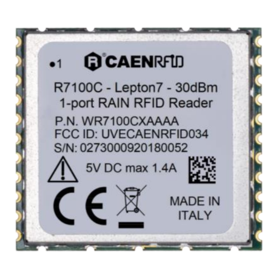
1 INTRODUCTION Description Reader The Lepton (Model R7100C), an embedded reader of the easy2read © product line, is an ultra compact reader for low power, high performance RAIN RFID applications. With programmable output power from 10dBm to 30dBm, the reader can detect tags at more than 5 mt of distance (depending on antenna and tag dimensions). -
Page 7: Technical Specifications
2 TECHNICAL SPECIFICATIONS Technical Specifications 865.600÷867.600 MHz (ETSI EN 302 208 v3.3.1) Frequency Range 902÷928 MHz (FCC part 15.247) Configurable from 10 dBm to 30 dBm (from 10 mW to 1W) conducted RF Power power RX Sensitivity -85dBm – 10%PER, assuming 20 dB antenna RL @ 30 dBm output Antenna VSWR <... -
Page 8: Key Features
Single mono-static RF port Field upgradability via firmware updates. Gen 2 v2 will be firmware upgradable UART serial interface using CAEN RFID easy2read © protocol Test features (CW, PRBS, custom regions, channel lists, and fixed frequency) -
Page 9: Hardware Interface
An example Lepton R7100C system-level block diagram for an embedded system is shown in Fig. 3.1: Lepton7 R7100C - Example of Block Diagram. This figure shows the electrical connections that may and must be made to control the Lepton R7100C. In the figure, the required connections are illustrated with solid lines. -
Page 10: Power Supply
Fig. 3.2: BSL sequence The BSL program execution starts when TST pin has received a minimum of two positive transitions and if TST is high while /RST rises from low to high. BSL_SEL shall be at high level before BSL starts. Pulses length and distance between edges of all signals shall be 10ms at least. -
Page 11: Reset Pin
Each of the UART interfaces signals at 3.3 V relative to GND. The specific VIH, VIL, VOH and VOL specifications may be found in the § Device Input and Output Specifications paragraph page 15. The TX pins are driven strong high and low with a sink/source current of about 8 mA. If the load on a pin draws more than the 8 mA sink and source current, the pin is not guaranteed to meet the VOH and VOL specs listed in §... -
Page 12: Wakeup Pin
Wakeup Pin The WKUP pin is used to wake the device when it is in the Standby or Sleep operating modes. This pin is edge sensitive and will wake the device on a rising edge. The WKUP pin must be logic low in order for the device to re-enter Idle mode after a Sleep wakeup, so it should only be pulsed high to wake up the part. -
Page 13: Electrical Specifications
Pin# Pin Name Pin Type Description RF antenna port Power Ground Digital I/O Reserved for Future Use BSL_SEL Digital Input Boot Strap Loader interface enable signal Power Ground Digital Input TST pin to be used for FW recovery/upgrade UART1-RX Digital Input R7100C UART Rx (Receive) from host UART1-TX Digital Output... -
Page 14: Operating Conditions
Operating Conditions This section describes operating voltage, frequency, and temperature specifications for the Lepton R7100C during operation. Parameter Min. Max. Unit Conditions Supply 4.75 5.25 VDC_IN relative to GND Temperature ºC Ambient Temperature FCC part 15.247 Frequency 865.6 867.6 ETSI EN 302 208 v3.3.1 Tab. -
Page 15: Uhf Gen 2 Rfid Radio Specifications
UHF Gen 2 RFID Radio Specifications Parameter Min. Typ. Max. Unit Conditions See § Tab. 2.1: Lepton7 R7100C Technical Frequency Specifications page 7 865.6 867.6 Input impedance Ω Input match 10%PER, assuming 20 dB antenna RL @ 30 Rx sensitivity dBm output Tab. -
Page 16: Tab. 3.9: Analog Interface Specification
Parameter Min. Typ. Max. Unit Conditions ADC (Pin 13) Resolution Bits Conversion voltage range Sampling rate 0.47 MSPs Total conversion time μsec Power-up time μsec Sampling switch resistance Ω Internal sample and hold capacitance Total unadjusted error ±3.5 ±7.1 Offset error ±3.0 ±5.6 Gain error... -
Page 17: Layout And Components
4 LAYOUT AND COMPONENTS Introduction This section describes hardware aspects of embedded RAIN RFID readers based on the Lepton R7100C. PCB Layout for RF 50 Ohm Characteristic Impedance As discussed in paragraph RF Connection page 10, a properly matched RF connection is critical to achieving high performance with Lepton R7100C. -
Page 18: Package And Assembly Information
In most PCB designs, many of the parameters of the PCB are already set, such as dielectric thickness and constant, trace conductivity and weight, etc. Usually, the only variables that can be easily modified are the style of transmission line, and its dimensions. The most common, and recommended PCB transmission line scheme is to use a microstrip on the top or bottom layer of the PCB, with a ground plane on the layer immediately adjacent as a return path. -
Page 19: Pcb Footprint
PCB Footprint Recommended footprint copper and pastemask dimensions are shown in the following: Fig. 4.3: Recommended Etched Copper Footprint – All Pads SMT Reflow Information The solder manufacturer’s recommended reflow profile is shown in the following figure: Fig. 4.4: Recommended Solder Reflow Profile for the Lepton R7100C LAYOUT AND COMPONENTS - Lepton - Technical Information Manual... -
Page 20: Moisture Sensitive Level 3 (Msl 3)
A. During PCB Assembly Devices are baked and dry-packed before shipment from CAEN RFID. The packing uses a Moisture Barrier Bag (MBB). A Humidity Indicator Card (HIC) and drying desiccant are included inside the MBB. A MSL 3 label is attached to caution that the bag contains moisture sensitive devices. -
Page 21: Regulatory Compliance
Consult the dealer or an experienced radio/TV technician for help. This transmitter module has been tested and found to comply with Part 15 of the FCC Rules. NOTE: a. Any changes or modifications not approved by CAEN RFID could void the user’s authority to operate the equipment. b. Lepton R7100C module is approved for operation with the following antenna: ... - Page 22 d. This transmitter module is authorized to be used in other devices only by OEM integrators under the following conditions: The RFID Module antenna shall have a separation distance of at least 20cm from all persons The transmitter module must not be co-located with any other antenna or transmitter e.
Need help?
Do you have a question about the Lepton7 R7100C and is the answer not in the manual?
Questions and answers