Table of Contents
Advertisement
RX-V620/HTR-5460
This manual has been provided for the use of authorized YAMAHA Retailers and their service personnel.
It has been assumed that basic service procedures inherent to the industry, and more specifically YAMAHA Products, are already
known and understood by the users, and have therefore not been restated.
WARNING:
IMPORTANT:
The data provided is believed to be accurate and applicable to the unit(s) indicated on the cover. The research, engineering, and
service departments of YAMAHA are continually striving to improve YAMAHA products. Modifications are, therefore,
inevitable and specifications are subject to change without notice or obligation to retrofit. Should any discrepancy appear to exist,
please contact the distributor's Service Division.
WARNING:
IMPORTANT:
CONTENTS
TO SERVICE PERSONNEL ........................................... 1
FRONT PANELS ............................................................. 2
REAR PANELS ......................................................... 3 - 4
SPECIFICATIONS ..................................................... 5 - 7
INTERNAL VIEW ............................................................ 7
DISASSEMBLY PROCEDURES ............................ 8 - 10
SELF DIAGNOSIS FUNCTION ............................. 11 - 29
AMP CHECK ................................................................. 30
1 0 0 7 6 0
RX-V620RDS
SERVICE MANUAL
IMPORTANT NOTICE
Failure to follow appropriate service and safety procedures when servicing this product may result in personal
injury, destruction of expensive components, and failure of the product to perform as specified. For these
reasons, we advise all YAMAHA product owners that any service required should be performed by an
authorized YAMAHA Retailer or the appointed service representative.
The presentation or sale of this manual to any individual or firm does not constitute authorization, certification
or recognition of any applicable technical capabilities, or establish a principle-agent relationship of any
form.
Static discharges can destroy expensive components. Discharge any static electricity your body may have
accumulated by grounding yourself to the ground buss in the unit (heavy gauge black wires connect to this
buss).
Turn the unit OFF during disassembly and part replacement. Recheck all work before you apply power to the
unit.
IC DATA ................................................................ 31 - 38
DISPLAY DATA .................................................... 39 - 40
PIN CONNECTION DIAGRAM ..................................... 41
BLOCK DIAGRAM ................................................ 42 - 45
PRINTED CIRCUIT BOARD ................................. 46 - 69
SCHEMATIC DIAGRAM ....................................... 70 - 75
PARTS LIST .......................................................... 76 - 94
REMOTE CONTROL TRANSMITTER .................. 95 - 97
AV RECEIVER
Advertisement
Table of Contents

Related Manuals for Yamaha RX-V620


Summary of Contents for Yamaha RX-V620
-
Page 1: Table Of Contents
This manual has been provided for the use of authorized YAMAHA Retailers and their service personnel. It has been assumed that basic service procedures inherent to the industry, and more specifically YAMAHA Products, are already known and understood by the users, and have therefore not been restated. -
Page 2: To Service Personnel
RX-V620/HTR-5460/RX-V620RDS TO SERVICE PERSONNEL 1. Critical Components Information Components having special characteristics are marked Z AC LEAKAGE EQUIPMENT and must be replaced with parts having specifications equal WALL TESTER OR OUTLET UNDER TEST EQUIVALENT to those originally installed. 2. Leakage Current Measurement (For 120V Models Only) -
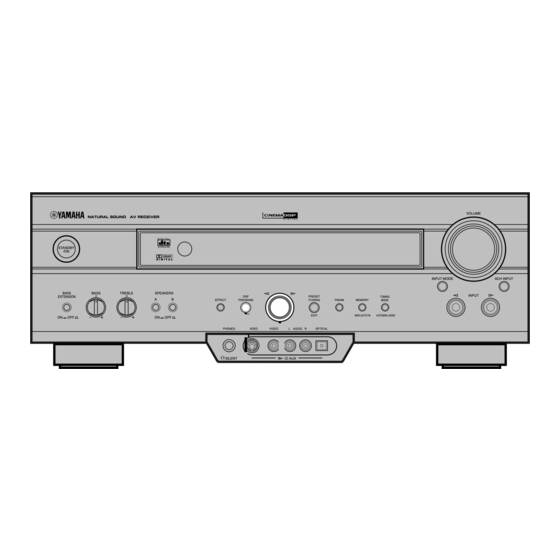
Page 3: Front Panels
RX-V620/HTR-5460/RX-V620RDS FRONT PANELS RX-V620/HTR-5460 VOLUME D I G I T A L D I G I T A L SURROUND STANDBY INPUT MODE 6CH INPUT BASS BASS TREBLE SPEAKERS INPUT EXTENSION PRESET TUNING EFFECT PROGRAM /TUNING FM/AM MEMORY MODE EDIT... -
Page 4: Rear Panels
RX-V620/HTR-5460/RX-V620RDS REAR PANELS RX-V620/HTR-5460 U model RX-V620/HTR-5460 C model RX-V620 R model, RX-V620/HTR-5460 T model 240V RX-V620 L model... - Page 5 RX-V620/HTR-5460/RX-V620RDS RX-V620/HTR-5460 A model RX-V620RDS B model RX-V620RDS G model...
-
Page 6: Specifications
RX-V620/HTR-5460/RX-V620RDS SPECIFICATIONS Signal-to-Noise Ratio (IHF-A-Network) AUDIO SECTION PHONO MM to REC OUT, Input Shorted 5mV U, C, R, T models ......86dB Minimum RMS Output Power per Channel A, B, G, L models . - Page 7 435 (17–1/8") Finish RX-V620 ... Black color (U, C, R, T, A models) Gold color (R, T, L models) RX-V620RDS ....Black color (B, G models)
-
Page 8: Internal View
RX-V620/HTR-5460/RX-V620RDS SET MENU TABLE SET MENU PRESET VALUE SETTING RANGES SPEAKER SET CENTER SPEAKER LARGE LARGE/SMALL/NONE MAIN SPEAKER LARGE LARGE/SMALL REAR L/R SPEAKER LARGE LARGE/SMALL/NONE LFE/BASS OUT BOTH SUBWOOFER/MAIN/BOTH MAIN LEVEL NORMAL NORMAL/–10dB L/R BALANCE L — 0 — R (0.5 step) (L/R 10.0) -
Page 9: Disassembly Procedures
RX-V620/HTR-5460/RX-V620RDS DISASSEMBLY PROCEDURES (Remove parts in the order as numbered.) 1. Removal of Top Cover Remove 8 screws ( q and w ) and then remove the Top Cover in Fig. 1. 2. Removal of Front Panel Unit a. Remove 9 screws ( e, r and t ) in Fig. 1. - Page 10 RX-V620/HTR-5460/RX-V620RDS 5. Removal of Input (1)/(2) P.C.B. (Checking the Input (1)/(2) P.C.B. and Replacing Components) a. Remove the DSP P.C.B. b. Remove 3 screws ( !0 ) and then remove the AM/FM Tuner in Fig. 4. c. Remove 2 screws ( !1 ) and then remove the Operation (5) P.C.B. in Fig. 4.
- Page 11 RX-V620/HTR-5460/RX-V620RDS 6. Removal of Main Chassis (Checking the Main (1) P.C.B. and Replacing Components) a. Remove the Front Panel Unit. b. Remove the Sub Chassis Unit. c. Remove the DSP P.C.B. d. Remove the AM/FM Tuner, Operation (5)/(3)/(2) P.C.B. and Input (1)/(2) P.C.B.
-
Page 12: Self Diagnosis Function
RX-V620/HTR-5460/RX-V620RDS SELF DIAGNOSIS FUNCTION This product has a built-in self diagnosis function (DIAG) to facilitate inspection, measurement and determination of a faulty item, if any. There are 14 DIAG menu items each of which has sub-menu items. Listed in the table below are menu items and sub-menu items. - Page 13 RX-V620/HTR-5460/RX-V620RDS Starting DIAG Press the “POWER” (STANDBY/ON) key of the main unit while pressing the “FM/AM” key and the “INPUT MODE” key simultaneously, and DIAG will be activated. Starting DIAG in the protection cancel mode If the protection function activates and causes hindrance to trouble diagnosis, disable the protection function as described below, and it will be possible to enter the DIAG mode.
- Page 14 RX-V620/HTR-5460/RX-V620RDS If the protection function activates after DIAG has been started and the power is turned off ; When the protection function (*2) activates, the protection function history appears on the display and the power turns off. Repair the faulty parts according to the displayed history.
-
Page 15: Main
RX-V620/HTR-5460/RX-V620RDS Operation procedure of DIAG menu and SUB-MENU There are 14 MENU items and some SUB-MENU items as well. DIAG menu selection Main unit: Jog dial w(forward)/q(reverse) EFFECT PROGRAM Remote control unit: Cursor N(forward)/B(reverse) key SUB-MENU selection Main unit: DSP PROGRAM (forward)/EFFECT (reverse) key <... - Page 16 RX-V620/HTR-5460/RX-V620RDS Details of DIAG menu 1. DSP THROUGH There are 6 sub menu items. ANALOG BYPAS [Remote control code: 7A—88(PRG 1)] 1.ANALOG BYPAS • The input mode is fixed to use the analog (A/D) system. • The L/R signal is output through the analog bypass without using the DSP section.
-
Page 17: Center
RX-V620/HTR-5460/RX-V620RDS M, C, R, SW CH [Remote control code: 7A—89 (PRG 2)] 1.M C R SW CH • The input signal is automatically identified and switched in the priority order of dts DOLBY DIGITAL PCM AUDIO Analog (A/D) according to the signal detection. - Page 18 RX-V620/HTR-5460/RX-V620RDS MAIN HPF [Remote control code: 7A—8A (PRG 3)] 1.MAIN HPF MAIN HPF is turned on and output. (Head margin included) Head margin MAIN L/R: 0/-3/-12/-18 dBF CENTER: Mute FL/FR: Mute RL/RR: Mute SWFR: Mute Reference INPUT : DVD ANALOG...
- Page 19 RX-V620/HTR-5460/RX-V620RDS FULL BIT F [Remote control code: 7A—92 (PRG 11)] 1.FULL BIT F The front channel signal is output in full bit to the main channel. Reference INPUT : DVD ANALOG SWFR: 50Hz, Others: 1kHz SPEAKERS Condition MAIN L/R CENTER...
- Page 20 RX-V620/HTR-5460/RX-V620RDS FULL BIT-6dB [Remote control code: 7A—03 (TAPE STOP)] 1.FULL BIT-6DB The head margin is included and the digital data is output in half bit. Head margin MAIN L/R: -6 dBFS CENTER: -6 dBFS FL/FR: Mute RL/RR: -6 dBFS SWFR: Add L/R signal at -6 dBFS.
- Page 21 RX-V620/HTR-5460/RX-V620RDS 2. FRONT CH • The input signal is automatically identified and switched in the priority order of dts DOLBY DIGITAL PCM AUDIO Analog (A/D) according to the signal detection. • The front channel signal is output to the main channel.
- Page 22 RX-V620/HTR-5460/RX-V620RDS 3. RAM THROUGH • The input signal is automatically identified and switched in the priority order of dts DOLBY DIGITAL PCM AUDIO Analog (A/D) according to the signal detection. • C, RL/RR and FL/FR signals are output through the external DRAM.
- Page 23 RX-V620/HTR-5460/RX-V620RDS (2ch) *Multi: All Mute AC3D3 YSS928 ANALOG CODEC -3dB SDOB0 (A/D) MAIN AK4527 AK4382 (Decoder) DD/dts SUB DSP DECODER DIGITAL CODEC C/Mute SDOB1 -3dB/Mute (D/A) SWFR AK4527 SDOB2 Mute SDOB3 -12dB 4M DRAM 5. MARGIN CHECK • The input signal is automatically identified and switched in the priority order of dts...
- Page 24 RX-V620/HTR-5460/RX-V620RDS 6. MAIN MIX • The input signal is automatically identified and switched in the priority order of dts DOLBY DIGITAL PCM AUDIO Analog (A/D) according to the signal detection. • There are two sub-menu items. • The center and SW signals are output through the main channel.
- Page 25 RX-V620/HTR-5460/RX-V620RDS 7. OTHER INPUT The signal input through the 6CH INPUT terminals is output. EXTERNAL DEC [Remote control code: 7A—8F (PRG 8)] 7.EXTERNAL DEC Reference INPUT : 6CH INPUT SWFR: 50Hz, Others: 1kHz SPEAKERS Condition MAIN L/R CENTER REAR L/R...
- Page 26 RX-V620/HTR-5460/RX-V620RDS 9. MANUAL TEST The test noise is output by the noise generator with a built-in DSP from the channels specified by the sub-menu. There are seven sub-menu items. The noise frequency is 35 - 250Hz for LFE and 800Hz as the center frequency otherwise.
- Page 27 RX-V620/HTR-5460/RX-V620RDS PRESET STATIONS STATION FM FACTORY PRESET DATA (MHz) STATION AM FACTORY PRESET DATA (kHz) PAGE U, C, R, T R, T, L, G, B, A PAGE U, C, R, T R, T, L, G, B, A, J 87.5 87.5 76.0...
- Page 28 RX-V620/HTR-5460/RX-V620RDS 12. IF STATUS (Input function status) Using this menu, the status data is displayed in the hexadecimal notation one after another. During signal processing, the status before execution of this menu is maintained. To convert the analog input to the digital input, use the following procedure.
- Page 29 RX-V620/HTR-5460/RX-V620RDS 5th byte Indicate Indicates the information on the signal processing status. 0 0 0 0 0 0 0 0 bit7 MUTE requested 7 6 5 4 3 2 1 0 bit6 dts flashing (Red) bit5 EX sound field being processed...
- Page 30 RX-V620/HTR-5460/RX-V620RDS 13. DSP RAM CHECK [Remote control code: 7A—0A (CD SKIP +)] This menu is used to self-diagnose whether or not YSS928 (IC801 of DSP circuit board) and external RAM (IC802 of DSP circuit board) are connected properly. During signal processing, the status before execution of this menu is maintained.
-
Page 31: Amp Check
RX-V620/HTR-5460/RX-V620RDS AMP CHECK Confirmation of Idling Current 1) No signal applied. 2) Non-loaded condition. 3) Aging is not neccessary. Cut OFF Test Point Note Item Rating (DC) MAIN L R145 If the measured voltage exceeds 10.1mV, cut MAIN R R150... -
Page 32: Ic Data
RX-V620/HTR-5460/RX-V620RDS IC DATA IC501 : µPD784217AGF (OPERATION P.C.B.) 16 bit µ-COM (CPU) P85/A5 P06/INTP6 P86/A6 P05/INTP5 P87/A7 P04/INTP4 P40/AD0 P03/INTP3 P41/AD1 P02/INTP2/NMI P42/AD2 P01/INTP1 P43/AD3 P00/INTP0 P44/AD4 RESET P45/AD5 P46/AD6 P47/AD7 P50/A8 P51/AD9 P52/AD10 P53/AD11 P127/RTP7 P54/AD12 P126/RTP6 P55/AD13 P125/RTP5... - Page 33 RX-V620/HTR-5460/RX-V620RDS IC501 : µPD784217AGF (OPERATION P.C.B.) 16 bit µ-COM (CPU) No. PORT Name I/O Function o. PORT Name I/O Function P60/A16 TC74HC164 CLOCK 100 Vss Ground P61/A17 99 P57/A15 O LC78211/LC78213 CE P62/A18 98 P56/A14 O NC P63/A19 97 P55/A13...
- Page 34 RX-V620/HTR-5460/RX-V620RDS IC801 : YSS928 (DSP P.C.B.) AC3D3 RAMA10 RAMD2 RAMA11 RAMD1 RAMD0 VDD2 VDD2 SELI8 SELI7 OPORT7 SELI6 OPORT6 SELI5 OPORT5 RAMA12 OPORT4 RAMA13 OPORT3 RAMA14 OPORT2 RAMA15 OPORT1 RAMA16 OPORT0 RAMA17 ZEROBF2L OVFB/END ZEROBF2R ZEROFLG ZEROBF3L ZEROBF3R NONPCM VDD1...
- Page 35 RX-V620/HTR-5460/RX-V620RDS IC801 : YSS928 (DSP P.C.B.) AC3D3 Name Function Crystal oscillator connecting terminal Crystal oscillator connecting terminal (24.576MHz ) SELI1 Built-in selector input 1 (AXD) SELI0 Built-in selector input 0 (GND) SELOA Built-in selector output A (ISEL) SELOB Built-in selector output B...
- Page 36 RX-V620/HTR-5460/RX-V620RDS IC801 : YSS928 (DSP P.C.B.) AC3D3 Name Function SDWCKI1 Word clock input terminal for SDIB, SDOB interface (Unconnected) SDBCKI1 Bit clock input terminal for SDIB, SDOB interface (Unconnected) Ground terminal SDOB3 PCM output terminal from Sub DSP SDOB2 PCM output terminal from Sub DSP...
- Page 37 RX-V620/HTR-5460/RX-V620RDS IC801 : YSS928 (DSP P.C.B.) AC3D3 Name Function RAMA5 Sub DSP: External memory address terminal 5 RAMA2 Sub DSP: External memory address terminal 2 SELI13 Built-in selector input 13 (Unconnected) SELI12 Built-in selector input 12 (Unconnected) SELI11 Built-in selector input 11 (Unconnected)
- Page 38 RX-V620/HTR-5460/RX-V620RDS IC587 : LC74781-9798 (OPERATION P.C.B.) Superimpose VSS1 VDD1 XTAL IN XTAL OUT CTRL3 CTRL1 CTRL2 BLANK SEP IN OSC IN SEP OUT OSC OUT SEPC CHARA SYN IN VDD1 SCLK CV IN VDD2 CV OUT SERIAL 8 BIT LATCH...
- Page 39 RX-V620/HTR-5460/RX-V620RDS IC587 : LC74781-9798 (OPERATION P.C.B.) Superimpose Pin No. Symbol Terminal name Function Ground terminal Connection to GND (Digital system ground terminal) VSS1 Crystal oscillation Terminal to connect the crystal of the crystal oscillator for internal synchronous XTAL IN terminal signal generation and a capacitor or to input an external clock.
-
Page 40: Display Data
RX-V620/HTR-5460/RX-V620RDS DISPLAY DATA V501 : 10-BT-236GNK (V6785800) PATTERN AREA PIN CONNECTION Pin No. Connection F1 NP NP P1 P2 P3 P4 P5 P6 P7 P8 P9 P10 P11 P12 P13 P14 P15 P16 P17 P18 P19 P20 P21 P22 P23 P24 P25 P26 Pin No. - Page 41 RX-V620/HTR-5460/RX-V620RDS ANODE CONNECTION...
-
Page 42: Pin Connection Diagram
RX-V620/HTR-5460/RX-V620RDS PIN CONNECTION DIAGRAM µPC29M33T-E1 NJM78L05A-T3 NJM79M05FA NJM7805FA PQ025EZ5MZP TC74HCU04AP TC74HC4053AP NJM79M12FA NJM7812FA 1: VIN 1:OUTPUT 1: INPUT 2: VC 1:COMMON 2:COMMON 2: GND 1: OUTPUT 3: VO 2:INPUT 3: OUTPUT 3:INPUT 2: COMMON 4: NC 3:OUTPUT 4: GND 5: GND... -
Page 43: Block Diagram
RX-V620/HTR-5460/RX-V620RDS BLOCK DIAGRAM D743-746 T741 See page 70 (DSP) XL801 CONVERTER COAXIAL IC801 YSS928 IC808A IC808B IC811A Q741 SDOB0 L (DAL) See page 75 (POWER) – IC815 AK4382 IC811B SIGNAL R (DAR) CXDTA – DETECTOR IC808C IC705 D723 IC703 OPTICAL... - Page 44 RX-V620/HTR-5460/RX-V620RDS BLOCK DIAGRAM CONTROL IC581A C-INPUT IC584B Q584 SELECTOR D-TV/CBL IC582 Q581 Y-INPUT SELECTOR VCR 1 IC583 Q583 IC585 Q585 VCR 2 VIDEO OUTPUT Q586 – 589 EXPANSION VIDEO HP-RELAY IC586 CONTROL IC584A SP-RELAY XL501 10MHz 87-90 XL581 Q587 IC588...
- Page 45 RX-V620/HTR-5460/RX-V620RDS PRINTED CIRCUIT BOARD (Foil side) Point q (Pin 1 of IC801) DSP P. C. B. (Lead Type Device) V : 2V/div, H : 50 nsec/div DC, 1 : 1 probe FROM : INPUT (1) Semiconductor Location Ref. No. Location Ref.
-
Page 46: Subwoofer
RX-V620/HTR-5460/RX-V620RDS PRINTED CIRCUIT BOARD (Foil side) Semiconductor Location INPUT ( 1 ) P. C. B. (Lead Type Device) Ref. No. Location IC301 IC302 IC303 FROM : INPUT (2) IC304 IC308 FROM : INPUT (2) FROM : DSP FROM : TUNER Ref. -
Page 47: Printed Circuit Board
RX-V620/HTR-5460/RX-V620RDS PRINTED CIRCUIT BOARD (Foil side) Semiconductor Location Ref. No. Location D301 Ref. No. Location IC311 INPUT ( 1 ) P. C. B. (Surface Mount Device) IC312 IC313 IC314 IC315 IC316 IC317 IC319 IC320 Ref. No. Location Q301 RDS only... - Page 48 RX-V620/HTR-5460/RX-V620RDS PRINTED CIRCUIT BOARD (Foil side) INPUT ( 2 ) P. C. B. INPUT ( 2 ) P. C. B. INPUT ( 3 ) P. C. B. (Lead Type Device) (Surface Mount Device) (Lead Type Device) INPUT ( 3 ) P. C. B.
- Page 49 RX-V620/HTR-5460/RX-V620RDS PRINTED CIRCUIT BOARD (Foil side) OPERATION ( 2 ) P. C. B. (Lead Type Device) 6CH INPUT S–VIDEO R, T only OPERATION ( 2 ) P. C. B. (Surface Mount Device) Semiconductor Location Ref. No. Location Ref. No. Location...
- Page 50 RX-V620/HTR-5460/RX-V620RDS PRINTED CIRCUIT BOARD (Foil side) Point w (Pin 38 of IC501) OPERATION ( 1 ) P. C. B. V : 2V/div, H : 0.1 µsec/div (Lead Type Device) DC, 1 : 1 probe TO : OPE (9) #505 W505...
- Page 51 RX-V620/HTR-5460/RX-V620RDS PRINTED CIRCUIT BOARD (Foil side) Semiconductor Location OPERATION ( 1 ) P. C. B. (Surface Mount Device) Ref. No. Location D501 D502 D503 D504 D505 D506 D507 U, C, R, T only D508 D509 R, T, A, L, B, G only...
- Page 52 RX-V620/HTR-5460/RX-V620RDS PRINTED CIRCUIT BOARD (Foil side) OPERATION ( 6 ) P. C. B. OPERATION ( 5 ) P. C. B. (Lead Type Device) (Lead Type Device) OPERATION ( 5 ) P. C. B. VIDEO AUX SILENT (Surface Mount Device) W711...
- Page 53 RX-V620/HTR-5460/RX-V620RDS PRINTED CIRCUIT BOARD (Foil side) Semiconductor Location MAIN ( 1 ) P. C. B. Ref. No. Location Ref. No. Location D101 Q101 D102 Q102 FROM : OPE (1) D103 Q103 PRVI D104 Q104 D105 Q105 D106 Q106 TO : MAIN (3)
- Page 54 RX-V620/HTR-5460/RX-V620RDS PRINTED CIRCUIT BOARD (Foil side) MAIN ( 5 ) P. C. B. MAIN ( 2 ) P. C. B. FROM : MAIN (1) W372 TO : MAIN (6) W109 TO : MAIN (1) –12 –25 –5 FROM : POWER (3)
- Page 55 RX-V620/HTR-5460/RX-V620RDS PRINTED CIRCUIT BOARD (Foil side) R, T models U, C, A, B, G, L models POWER ( 2 ) P. C. B. POWER ( 1 ) P. C. B. POWER ( 1 ) P. C. B. TO : POWER (3)
- Page 56 RX-V620/HTR-5460/RX-V620RDS PRINTED CIRCUIT BOARD (Foil side) U, C, A, B, G, L models R, T models POWER ( 5 ) P. C. B. POWER ( 6 ) P. C. B. POWER ( 4 ) P. C. B. TO : POWER (1)
-
Page 57: Schematic Diagram
RX-V620/HTR-5460/RX-V620RDS SCHEMATIC DIAGRAM (DSP) P-71 Point q (Pin 1 of IC801) to INPUT (1) V : 2V/div, H : 50 nsec/div DC, 1 : 1 probe DRAM 11.9 –11.2 –11.3 IC803 : PQ025EZ5MZP +2.5V Regulator DC INPUT (VIN) DC OUTPUT (VO) ON/OFF CONTROL (VC) –11.2... - Page 58 RX-V620/HTR-5460/RX-V620RDS SCHEMATIC DIAGRAM (INPUT 1/2) P-E73 P-E72 P-E72 P-E72 PHONO MM EQ AMP 10.7 11.2 11.2 RJ-1073F-09-0351A –0.1 –0.1 –11.2 –11.8 –11.1 –10.6 –11.8 11.2 11.2 IC301, 303 : LC78211 P-E74 Analog Function Switch –11.8 –11.8 –0.1 –11.8 L1 1 –0.1...
- Page 59 RX-V620/HTR-5460/RX-V620RDS SCHEMATIC DIAGRAM (INPUT 2/2 & OPERATION 1/2) 11.9 11.9 P-E71 11.9 11.3 –5.7 –5.7 –5.7 –5.7 –5.1 –11.9 –5.1 –20.5 LEVEL CONTROL –28.2 –14.4 –24.5 –24.5 –24.5 –10.9 –27.8 –28.2 –24.8 –24.8 –24.8 –5.1 –24.4 FL DRIVER –27.8 –24.5 –5.1...
- Page 60 RX-V620/HTR-5460/RX-V620RDS SCHEMATIC DIAGRAM (OPERATION 2/2) SAME PAGE SAME PAGE IC581 : TK15420M X : NOT USED VIdeo Amp CIRCUIT CHANGES BY MARKET. O : USED –IN – – –IN INPUT SELECTOR IC588 : LA7109 Ω Video Driver VIN1+ +VCC1 NFB1...
- Page 61 RX-V620/HTR-5460/RX-V620RDS SCHEMATIC DIAGRAM (MAIN 1/2) POWER AMP (L ch) 54.2 P-E73 54.1 53.8 52.4 53.3 53.3 53.9 53.9 54.2 41.8 35.0 41.8 41.8 53.9 35.1 34.5 35.0 –0.4 35.6 29.8 –1.0 35.6 –0.5 53.1 –0.5 –1.0 –54.2 –1.0 52.6 –54.2 –53.0...
- Page 62 RX-V620/HTR-5460/RX-V620RDS SCHEMATIC DIAGRAM (MAIN 2/2 & POWER) CIRCUIT CHANGES BY MARKET. O : USED X : NOT USED X : NOT USED CIRCUIT CHANGES BY MARKET. O : USED POWER SUPPLY SAME PAGE 12.5 12.5 12.6 P-E74 SAME PAGE POWER SUPPLY –54.3...
-
Page 63: Parts List
RX-V620/HTR-5460/RX-V620RDS WARNING PARTS LIST Components having special characteristics are marked Z and must be replaced with parts having specifications equal to those originally installed. Carbon resistors (1/6W or 1/4W) are not included in the ELECTRICAL PARTS ELECTRICAL PARTS List. For the parts No. of the carbon resistors, refer to last page. - Page 64 RX-V620/HTR-5460/RX-V620RDS P.C.B. INPUT Schm Schm Ref. PART NO. Description Market Ref. PART NO. Description Market V7209500 P.C.B. INPUT UCRT C338 UR837100 C.EL 10uF 16V V7209600 P.C.B. INPUT C339 UR837100 C.EL 10uF 16V V7209700 P.C.B. INPUT C341 VD930900 C.CE.SMI 0.1uF 25V V7209800 P.C.B. INPUT C342 VD930900 C.CE.SMI 0.1uF 25V...
- Page 65 RX-V620/HTR-5460/RX-V620RDS P.C.B. INPUT Schm Schm Ref. PART NO. Description Market Ref. PART NO. Description Market C423 UR837100 C.EL 10uF 16V C513 UR837470 C.EL 47uF 16V C424 VG287200 C.EL 10uF 50V C514 UT652100 C.PP 100pF 100V C425 UR837100 C.EL 10uF 16V C515 UR866220 C.EL 2.2uF 50V C428 UU137100 C.EL 10uF 16V...
- Page 66 RX-V620/HTR-5460/RX-V620RDS P.C.B. INPUT & OPERATION Schm Schm Ref. PART NO. Description Market Ref. PART NO. Description Market * PJ304 V7046700 JACK.PIN MSP‑244V1‑01NI CB504 VP682200 CN.BS.PIN 8P * PJ305 V7189700 JACK.PIN CB505 Vi879000 CN.BS.PIN 12P Q301 VD303700 TR 2SC3326 A,B CB506 Vi878000 CN.BS.PIN 2P...
- Page 67 RX-V620/HTR-5460/RX-V620RDS P.C.B. OPERATION Schm Schm Ref. PART NO. Description Market Ref. PART NO. Description Market C599 UR837470 C.EL 47uF 16V C692 UR827470 C.EL 47uF 10V C600 UR837470 C.EL 47uF 16V C693 UR827470 C.EL 47uF 10V C601 US135100 C.CE.CHP 0.1uF 16V C694 US135220 C.CE.CHP 0.22uF 16V C602 US135100 C.CE.CHP 0.1uF 16V...
- Page 68 RX-V620/HTR-5460/RX-V620RDS P.C.B. OPERATION & DSP Schm Schm Ref. PART NO. Description Market Ref. PART NO. Description Market IC503 XJ757A00 IC NJM78L05A‑T3 SW502 V4586200 SW.RT.ENC REB161PVB20F IC581 XW939A00 IC TK15420M VIDEO AMP SW503 VG392900 SW.TACT SKHVAA * IC582 XY549A00 IC TC74HC4051AFEL SW504 VG392900 SW.TACT SKHVAA...
- Page 69 RX-V620/HTR-5460/RX-V620RDS P.C.B. DSP Schm Schm Ref. PART NO. Description Market Ref. PART NO. Description Market C822 US135100 C.CE.CHP 0.1uF 16V C875 US061470 C.CE.M.CHP 47pF 50V C823 US135100 C.CE.CHP 0.1uF 16V C876 US061470 C.CE.M.CHP 47pF 50V C824 US135100 C.CE.CHP 0.1uF 16V C877 US061470 C.CE.M.CHP 47pF 50V C825 US061100 C.CE.M.CHP 10pF 50V C878 US061470 C.CE.M.CHP 47pF 50V...
- Page 70 RX-V620/HTR-5460/RX-V620RDS P.C.B. DSP Schm Schm Ref. PART NO. Description Market Ref. PART NO. Description Market C928 UU147100 C.EL 10uF 25V D819 VT332900 DIODE 1SS355 C929 UU147100 C.EL 10uF 25V D820 VT332900 DIODE 1SS355 C930 UU137470 C.EL 47uF 16V D821 VT332900 DIODE 1SS355 C931 UU137470 C.EL 47uF 16V...
- Page 71 RX-V620/HTR-5460/RX-V620RDS P.C.B. DSP & MAIN Schm Schm Ref. PART NO. Description Market Ref. PART NO. Description Market Q817 VD303700 TR 2SC3326 A,B C120 VR325000 C.MYLAR 100pF 100V Q818 VD303700 TR 2SC3326 A,B C121 UU137470 C.EL 47uF 16V R842 HV753100 R.CAR.FP 1Ω 1/4W C122 VR325000 C.MYLAR 100pF 100V R843 HV753100 R.CAR.FP...
- Page 72 RX-V620/HTR-5460/RX-V620RDS P.C.B. MAIN Schm Schm Ref. PART NO. Description Market Ref. PART NO. Description Market C271 VQ245400 C.PP 33pF 200V D112 VN008700 DIODE 1SS270A C272 VG291300 C.EL 100uF 50V D113 VD631600 DIODE 1SS133,176 C273 UA653100 C.MYLAR 1000pF 50V D114 VD631600 DIODE 1SS133,176 C274 VQ245400 C.PP 33pF 200V...
- Page 73 RX-V620/HTR-5460/RX-V620RDS P.C.B. MAIN Schm Schm Ref. PART NO. Description Market Ref. PART NO. Description Market Q113 V4096100 TR 2SC4614 S,T R112 V3945600 R.MTL.OXD 1KΩ 0.5W Q114A iX630850 TR 2SA1695 O,P,Y R113 V3945500 R.MTL.OXD 820Ω 0.5W Q114C iX630860 TR 2SC4468 O,P,Y R115 VP941600 R.MTL.OXD 5.6KΩ 1W Q116 V4096000 TR 2SA1770 S,T...
- Page 74 RX-V620/HTR-5460/RX-V620RDS P.C.B. MAIN & POWER Schm Schm Ref. PART NO. Description Market Ref. PART NO. Description Market R193 VP939800 R.MTL.OXD 10Ω 1W V7210100 P.C.B. POWER R203 VP939700 R.MTL.FLM 4.7Ω 1W V7210200 P.C.B. POWER R204 VP939700 R.MTL.FLM 4.7Ω 1W V7210300 P.C.B. POWER R205 VP940800 R.MTL.OXD 470Ω 1W V7210400 P.C.B.
- Page 75 RX-V620/HTR-5460/RX-V620RDS P.C.B. POWER & CHIP RESISTOR Schm Schm Ref. PART NO. Description Market Ref. PART NO. Description Market D746 VV307700 DIODE 1N4002S EP600140 SCR.BND.HD 3x10 MFZN2‑BL RT D747 VV307700 DIODE 1N4002S RD353100 R.CAR.CHP 1Ω 1/10W D748 VD631600 DIODE 1SS133,176 RD353220 R.CAR.CHP 2.2Ω 1/10W F741 VS822500 FUSE 2.0A 125V...
- Page 76 RX-V620/HTR-5460/RX-V620RDS EXPLODED VIEW U,C,A,B,G,L U,C model A model B model models only 9 (5) models only 9 (6) B,G models only 10 (7) R,T models G,L models 3-104 3-101 9 (3) 3-106 3-10 2-101 3-103 3-107 1-25 3-102 1-25 200-1...
- Page 77 RX-V620/HTR-5460/RX-V620RDS MECHANICAL PARTS Ref. PART NO. Description Remarks Markets * 1‑3 V7331800 S FLEXIBLE FLAT CABLE 37P 250mm P=1.25 * 1‑5 V6870900 FRONT PANEL RXV620BL * 1‑5 V6871000 FRONT PANEL RXV620GD * 1‑5 V6871100 FRONT PANEL RXV620RDSBL * 1‑5 V6871200 FRONT PANEL RXV620RDSGD * 1‑5 V6871300 FRONT PANEL RXV620RDSTI * 1‑5 V6871400 FRONT PANEL...
- Page 78 RX-V620/HTR-5460/RX-V620RDS Ref. PART NO. Description Remarks Markets V7209200 P.C.B. ASS'Y OPERATION V7209500 P.C.B. ASS'Y INPUT UCRT V7209600 P.C.B. ASS'Y INPUT V7209700 P.C.B. ASS'Y INPUT V7209800 P.C.B. ASS'Y INPUT V7209900 P.C.B. ASS'Y V7210100 P.C.B. ASS'Y POWER V7210200 P.C.B. ASS'Y POWER V7210300 P.C.B. ASS'Y POWER V7210400 P.C.B. ASS'Y POWER V7210500 P.C.B. ASS'Y POWER * 10 V7210700 P.C.B. ASS'Y...
-
Page 79: Remote Control Transmitter
RX-V620/HTR-5460/RX-V620RDS Ref. PART NO. Description Remarks Markets VQ775900 GROUND PLATE VS025000 LEG D60xH21 V620BL,V620TI V0042500 LEG D60xH21 V620GD,5460GD VV544300 LEG D60xH21 5460BL V6002200 KNOB D43 V6002300 KNOB D43 V6002400 KNOB D43 * 122 V6877900 KNOB/D18 * 122 V6878000 KNOB/D18 * 122 V6878100 KNOB/D18 V6001600 KNOB D15 V6001700 KNOB D15... - Page 80 RX-V620/HTR-5460/RX-V620RDS REMOTE CONTROL TRANSMITTER 7A15 7A16 7AC9 7AC1 7A54 7A0F 7A14 7A55 7A13 7ACA 7A87 7A18 7A11 7A10 7A85 7A12 7A98 A/B/C/D/E 7A53 7A52 7AC2 7A86 7A9C 7A1D 7A1E 7A1A 7A57 7A1B 7A1C KEY POSITION ONLY "AMP/TUNER" 0003 CODE Function Keychart...
- Page 81 RX-V620/HTR-5460/RX-V620RDS List of the Yamaha Code (NEC Format) DVD MENU Name Yamaha 0008 Yamaha 0008 Yamaha 0007 Yamaha 0005 Yamaha 0015 7C-94 7C-94 7C-17 79-11 79-11 7C-95 7C-95 7C-18 79-12 79-12 7C-96 7C-96 7C-19 79-13 79-13 7C-97 7C-97 7C-1A 79-14...
- Page 82 RX-V620/HTR-5460/RX-V620RDS SCHEMATIC DIAGRAM...
- Page 83 RX-V620/HTR-5460/RX-V620RDS Parts List for Carbon Resistors Value 1/4W Type Part No. 1/6W Type Part No. Value 1/4W Type Part No. 1/6W Type Part No. 1.0 Ω 3100 3100 7100 10 kΩ 7100 HJ35 HF85 HF45 HF45 1.8 Ω 3180 7110 11 kΩ...
- Page 84 RX-V620/HTR-5460/RX-V620RDS...
Need help?
Do you have a question about the RX-V620 and is the answer not in the manual?
Questions and answers