
Related Manuals for Lex 3I270D

Summary of Contents for Lex 3I270D
- Page 1 533MHz FSB / VGA / 4 LAN / Mini card Intel Atom N270 . 533MHz FSB . All-in-one . LAN . mini card for USB SATA . 8 USB . CF Multi-LAN Board NO. 3I270D Release date: July . 10 . 2009...
-
Page 2: Table Of Contents
2-2 UNPACKING CHECKUP ..................... 2-3 DIMENSION ........................ 2-4 LAYOUT - 3I270D ......................2-5 DIAGRAM - 3I270D ..................... 2-5-1 BOTTOM SIDE DIAGRAM - 3I270D ................ 2-6 INSTALL MEMORY ..................... 2-7 JUMPER SETTING DESCRIPTION ................2-8 COMS DATA SET ......................CHAPTER 3 CONNECTION .................. - Page 3 CHAPTER 4 INTRODUCTION OF BIOS ..............4-1 ENTER SETUP ......................4-2 GETTING HELP ......................4-3 THE MAIN MENU ....................... 4-4 STANDARD CMOS FEATURES ................4-5 ADVANCED BIOS FEATURES .................. 4-5-1 HARD DISK BOOT PRIORITY ................4-5-2 USB BOOT PRIORITY .................... 4-6 ADVANCED CHIPSET FEATURES ................
- Page 4 2009 July. 10. 2009...
-
Page 5: Warning
Warning ! 1. Battery Battery on board is consumables. We doesn’t guarantee the life time of it. 2. Fanless solution with HDD Please be aware of specification & limitation for HDD when fanless solution is implemented. 3. We will not give further notification if there is any change about the product information and the manual. -
Page 6: Hardware Notice Guide
Hardware Notice Guide 1. Before installing the power supply with this motherboard, please attach the 12V/DC ( 2 pin connector )of the adapter to motherboard first. After that, plug the adapter power to AC outlet. Always normally shut down the computer before you move the system unit or remove the power supply from the motherboard. - Page 7 Photo 1 Insert Unplug...
-
Page 8: Chapter 1 General Information
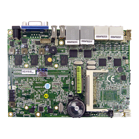
The 3I270D is an All-In-One Networking control Board. The board's design combines all necessary input and output interfaces, which make itself an ideal all-in-one control board for thin client, firewall or server applications. 3I270D is the perfect platform for a whole range of small form factor, low-power devices. -
Page 9: Major Feature
1-1 Major Feature 1. Intel Atom N270 CPU ( FSB 533 Mhz ) 2. Intel 945GSE Chipset on board, Graphic Chip Integrated 3. On board DDR2 module 1GB and support DDR2 SODIMM up to 2GB (option) 4. On board SSD 1/2/4/8 GB (option) 5. -
Page 11: Installing The So-Dimm
1-3 Installing the SO-DIMM 1. Align the SO-DIMM with the connector at a 45 degree angle. 2. Press the SO-DIMM into the connector until you hear a click. - Page 12 Notices: 1.The connectors are designed to ensure the correct insertion. If you feel resistance, check the connectors & golden finger direction, and realign the card. 2. Make sure the retaining clips (on two sides of the slot) lock onto the notches of the card firmly.
-
Page 13: 1-3-1.1 Removing The So-Dimm
1-3-1.1 Removing the SO-DIMM 1. Release the SO-DIMM by pulling outward the two retaining clips and the SO-DIMM pops up slightly. 2. Lift the SO-DIMM out of its connector carefully. -
Page 14: Directions For Installing The Mini Card
1-4 Directions for installing the Mini Card 2. Plug in the Mini Card in a 45 angle 1. Unscrew the screw on the board 3. Gently push down the Mini Card and screw the screw back. -
Page 15: Packing List
1-5 Packing List 5 USB Cable 1 3I270D Board 2 Utility CD Disk 6 DC Cable 7 User’s Manual 3 SATA Data Cable 8 DC 12V Power Adapter(2P) 4 SATA Power Cable The packing list above is for the users who purchase single motherboard. The users who purchase the board with chassis may refer to the packing list in the Assembly Guide. -
Page 16: Chapter 2 Hardware Installation
Please follow section 1-5, 2-1 and 2-2 to check the delivery package and unpack carefully. Please follow the jumper setting procedure. 2-1 Unpacking Precaution The 3I270D board has been well packed with an anti-static bag to protect its sensitive components and circuitry from damage due to static electric discharge. NOTE! 1. -
Page 17: Unpacking Checkup
2-2 Unpacking checkup First of all, please follow all necessary steps of section 2-1 to protect 3I270D from electricity discharge. With reference to section 1-5, please check the delivery package again with following steps: 1. Unpack the 3I270D board and keep all packing material, manual and driver disc etc, do not dispose ! 2. -
Page 18: Dimension
2-3 Dimension 57.02 35.43 21.84 3I270D_VR_V4G-M01 2.99 32.7 54.4 63.7 75.5 108.7 125.8 137.18... -
Page 19: Layout - 3I270D
Layout - 3I270D CFP1 MPCE1 CC21 SWP1 CPO1 LED1 FAN1 JSB1 CU61 CU31 CG11 CPI1 SODIM1 CPI13... -
Page 20: Diagram - 3I270D
Diagram - 3I270D CFP1 MPCE1 CF1 CC21 SWP1 CPO1 LED1 FAN1 JSB1 CG11 CPI1 SODIM1 CPI13... -
Page 21: Bottom Side Diagram- 3I270D
2-5-1 Bottom Side Diagram- 3I270D SATA1 SATA2 Back Panel-3I270D LAN 3 LAN 1 DC 12V IN LAN 4 LAN 2... -
Page 22: Install Memory
2-6 Install Memory This motherboard provides one 200-pin Small Outline Dual In-line Memory Module (SODIMM) socket for memory expansion available from minimum memory size of 256MB to maximum memory size of 2GB DDR2 SDRAM. DDR2 clock supports: DDR2 533, DDR2 667 Valid Memory Configurations Total Memory System Accept or Not... -
Page 23: Jumper Setting Description
NOTE! When you install SODIMM module fully into the SODIMM socket, the eject tab should be locked into the SODIMM module very firmly and fit into its indention on both sides. WARNING! Once you hear " Beep Beep Beep" sounds after turning on the power , please check if the DRAM is installed properly or not. -
Page 24: Coms Data Set
2-8 CMOS Data Set A battery must be used to retain the motherboard configuration in CMOS RAM. Close pin 1and pin 2 of JSB1 to store the CMOS data. To clear the CMOS, follow the procedures below: 1. Turn off the system and unplug the AC power 2. -
Page 25: Chapter 3 Connection
Chapter-3 Connection This chapter provides all necessary information of the peripheral's connections, switches and indicators. Always power off the board before you install the peripherals. 3-1 List of Connectors CA3: Line-out/Line-in/Mic-in 2x5 pin (2.0mm) Wafer CC1: COM1 DB9 Connector (Share to CG1) CC21: COM2 5pin (1.25mm) Wafer CF1: CF socket 50pin CFP1: FP ports 2x5 pin (2.0mm) Wafer... -
Page 26: Fan Connector
List of Connectors CU7: USB 7 port 4pin(1.25mm) Wafer CU8: USB 8 port 4pin(1.25mm) Wafer(Share to MPCE1) FAN1: CPU FAN 3pin Wafer LED1: power LED MPCE1: Mini card socket 52pin SATA1,SATA2: Two SATA connector 7pin 3-2 FAN Connector FAN1: CPU FAN connector(3pin 2.5mm wafer) PIN NO. -
Page 27: Vga Port Connector
*Note : VGA signal CG11 share with CG1 VGA CG1 3-4 Audio Port Connector The 3I270D has an on-board AC'97 3D sound interface. There are the connectors of LINE OUT, MIC-IN and CD-IN connectors. The MIC-IN Jack and CD-IN header are for audio sound input. The LINE-OUT pin1 connector is a 4-pin Jack for audio sound output. -
Page 28: Cf Card Reade
3-5 CF card Reade 3I270D configures CompactFlash Storage Card in IDE mode. It will use IDE channel when CompactFlash card is plugged in. This socket supports CF Card Type I/II socket spec. CF Socket 50pin--CF1 CF1: CF Socket For True IDE Mode (50pin CF Socket) PIN NO. -
Page 29: Usb Port
3-6 USB ports USB Ports (USB Type A connector) CU1: USB1, CU2: USB2 PIN NO Description PIN NO. Description CU1: USB1 DATA- DATA- DATA+ DATA+ CU2: USB2 CU31: USB 3 port 4pin Type A (Share to CL1) CU61: USB 6 port 4pin Type A (Share to CL2) pin1 pin1 pin1... -
Page 30: Lan Port
3-7 LAN port CL1 : LAN1 port RJ45 (Rear side connector Share to CU31) CL2 : LAN2 port RJ45 (Rear side connector Share to CU61) CL3 : LAN3 port RJ45 CL4 : LAN4 port RJ45 LAN port Giga /100Mb( RJ45 Jack) PIN NO Description PIN NO. -
Page 31: Com Port Connector (Oem)
3-8 COM Port Connector (OEM) CC1: RS232 Mode COM1 conector ( D-SUB 9pin) PIN NO. Description PIN NO. Description CC21 pin1 CC1: COM1 Note : All signal are RS-232 level. CC21: COM2 port (5pin 1.25mm Wafer) PIN NO. Note : All signal are TTL level . 3-9 For F75111N I2C watch dog timer device: DIO function: Logic 0 Level :+0.5V Max , Logic 1 Level : +4V Min... -
Page 32: I2C Wdt/Dio W75Io.h Reference Sample Code
3-10 I2C WDT/DIO W75IO.h Reference sample code: Compile platform:TC30 & DOS 6.22 // Sample.cpp : Defines the entry point for the console application. #include "stdafx.h" #include "conio.h" #include <string.h> #include <stdlib.h> #include <iostream> #include "W75IO.h" /* include W75IO.h #define DEMO_DI #define DEMO_DO #define... - Page 33 default: result=-1; break; (result == -1) return -1; (strlen(str) == 1 ) value=value+result; (strlen(str) == 2 ) ( i == 0 ) value=value+result*16; ( i == 1 ) value=value+result; return value; BOOL W75IO_init() /* First step :to init W75IO.DLL */ (InitializeW75IO()) /* init onboard W75IO chipset */ (InitInternalW75IO())
- Page 34 printf("read input input value %d\n",InterDigitalInput()); getch(); void W75IO_WDT() /* get WDT timer value*/ value; printf("Please enter WatchDog Timer value (0-255)\n"); cin>>value; /* check value */ timer=value; (timer > 255) printf("must be > 255\n"); getch(); return; /* sete onboard W75IO use secord as WatchDog Timer unit */ SetInterWDTUnit(FALSE);...
- Page 35 int main(int argc, char* argv[]) /* get user enter value*/ (W75IO_init()) while option =menu(); ( option == 4 ) break; switch (option) case DEMO_DI: W75IO_DI(); break; case DEMO_DO: W75IO_DO(); break; case DEMO_WDT: W75IO_WDT(); break; case DEMO_EXIT: break; return...
-
Page 36: I2C Wdt/Dio F75111N Reference Sample Code
3-10-1 I2C WDT/DIO F75111N reference sample code: Compile platform: Windows (include SMBus.h) Contents 1. Introduction 1.1 Initial Internal F75111 port address (0x9c) 1.2 Set F75111 DI/DO ( sample code as below Get Input value/Set output value) 1.3 Enable/Disable WDT 1.4 PULSE mode 2. - Page 37 2. Initial internal F75111 void F75111::InitInternalF75111() //set GPIO1X to Input function this->Write_Byte(F75111_INTERNAL_ADDR,GPIO1X_CONTROL_MODE ,0x00); //set GPIO3X to Input function this->Write_Byte(F75111_INTERNAL_ADDR,GPIO3X_CONTROL_MODE ,0x00); //set GPIO2X to Output function this->Write_Byte(F75111_INTERNAL_ADDR,GPIO2X_CONTROL_MODE ,0xFF); //Enable WDT OUT function this->Write_Byte(F75111_INTERNAL_ADDR,F75111_CONFIGURATION, 0x03); 3. Set output value void F75111::InterDigitalOutput(BYTE byteValue) BYTE byteData = 0;...
- Page 38 byteGPIO1X = byteGPIO1X & 0xF0; // Mask unuseful value byteGPIO3X = byteGPIO3X & 0x0F; // Mask unuseful value byteData = ( byteGPIO1X & 0x10 )? byteData + 0x01 : byteData; byteData = ( byteGPIO1X & 0x80 )? byteData + 0x02 : byteData; byteData = ( byteGPIO1X &...
- Page 39 7. Define F75111 pin in F75111.h //-------------------------------------------------------------------------------------------------------- #define F75111_INTERNAL_ADDR 0x9C // OnBoard F75111 Chipset #define F75111_EXTERNAL_ADDR 0x6E // External F75111 Chipset //-------------------------------------------------------------------------------------------------------- #define F75111_CONFIGURATION 0x03 // Configure GPIO13 to WDT2 Function //-------------------------------------------------------------------------------------------------------- #define GPIO1X_CONTROL_MODE 0x10 // Select Output Mode or Input Mode #define GPIO2X_CONTROL_MODE 0x20...
- Page 40 #define GP3_PSWIDTH_1MS 0x01 // When select Pulse mode: 1 #define GP3_PSWIDTH_20MS 0x02 // When select Pulse mode: 20 ms. #define GP3_PSWIDTH_100MS 0x03 // When select Pulse mode:100 ms. //-------------------------------------------------------------------------------------------------------- #define WDT_TIMER_RANGE 0x37 // 0-255 (secord or minute program by WDT_UNIT) #define WDT_CONFIGURATION 0x36...
- Page 41 Contents 1. Write_Byte Mode 2. Read_Byte Mode 3. Check Device (F75111) 4. SMBus_Clear 5 SMBus_Wait 6. SMBus_Busy 7. IO_Write 8. IO_Read 9. Define SMBus IO address 10. Define SMBus pin in SMBus. 1. Write Byte Mode int SMBus::Write_Byte(WORD dwSlave, BYTE pCmd, BYTE pByte) this->SMBus_Clear();...
- Page 42 int ret = this->SMBus_Wait(); // Check SMBus Status if (ret == SMBUS_OK) // If SMBus Stand by *pByte = (BYTE)this->IO_Read(SMBHSTDAT0) &0xFF; // Get SMBus host data value return ret; // reture SMBus status 3. Check Device (F75111) BOOL SMBus::CheckDevice(WORD wDeviceAddress) int ret;...
- Page 43 5. SMBus_Wait int SMBus::SMBus_Wait() timeout = SMBUS_TIMEOUT; DWORD dwValue; while (timeout--) Sleep(10); // I/O Delay dwValue = IO_Read(SMBHSTSTS) & 0x00FF; // Read Host Status Register if( dwValue & SMBHSTSTS_INTR ) // if status value equal SMBHSTSTS_INTR, return SMBus_OK return SMBUS_OK; // if status value equal SMBHSTSTS_FAILED, return SMBHSTSTS_FAILED if( dwValue &...
- Page 44 6. SMBus_Busy BOOL SMBus::SMBus_Busy() // Check SMBus status if equal SMBHSTSTS_BUSY if( (this->IO_Read(SMBHSTSTS) & SMBHSTSTS_BUSY ) == 1 ) return TRUE; // return true else return FALSE; // else retrun false 7. IO_Write void SMBus::IO_Write(WORD dwOffset, BYTE dwData) // Set dwData value to assigned address SetPortVal(this->m_MapIOAddress+dwOffset, dwData,1);...
- Page 45 10. Define SMBus pin in SMBus.h #define SMBHSTSTS 0x00 // SMBus Host Status Register Offset #define SMBHSTSTS_BUSY 0x01 // SMBus Host -> 0000-0001 Busy #define SMBHSTSTS_INTR 0x02 // SMBus Host -> 0000-0010 Interrupt / complection #define SMBHSTSTS_ERROR 0x04 // SMBus Host -> 0000-0100 Error #define SMBHSTSTS_COLLISION 0x08...
-
Page 46: Front Panel Port Header
3-11 Front Panel Port Header CFP1: FP connector (2x5pin 2.0mm wafer) pin1 SWP1 CFP1 pin1 PIN NO. Description PIN NO. Description HDD LED - HDD LED + LAN1 LED - LAN1 LED + LAN2 LED - LAN2 LED + LAN3 LED - LAN3 LED + LAN4 LED - LAN4 LED +... -
Page 47: Dc +5 /+12V Voltage Output Connector
3-13 DC +5 / +12V Voltage output connector CPO1: +12V / +5V DC voltage output (4pin 2.0mm Wafer) PIN NO. Description CPO1 pin1 +12V* *Note: DC in +12V by switch to DC-out voltage +12V, so DC in need stable +12V input 3-14 I C Bus Interface CO1: I C(SM) bus connector (4 pin 1.25mm wafer) (Option) PIN NO. -
Page 48: Mini Card
3-16 Mini card MPCE1 : Support USB Interface only (Mini card socket 52pin) Please refer to page 10 for installation of Mini card. MPCE1 3-17 SATA Interface SATA1,SATA2: Two SATA connector (7pin wafer) PIN NO. Description DATA TX+ DATA TX- DATA RX- DATA RX+ Note: BOM no SATA2 connector. - Page 49 Chapter 4 Introduction of BIOS The BIOS is a program located in the Flash Memory on the motherboard. This program is a bridge between motherboard and operating system. When you start the computer, the BIOS program gains control. The BIOS first operates an auto-diagnostic test called POST (Power on Self Test) for all the necessary hardware, it detects the entire hardware devices and configures the parameters of the hardware synchronization.
- Page 50 4-2 Getting Help Main Menu The on-line description of the highlighted setup function is displayed at the bottom of the screen. Status Page Setup Menu/ Option Page Setup Menu Press F1 to pop up a small help window that describes the appropriate keys to use and the possible selections for the highlighted item.
- Page 51 Standard CMOS Features This Menu is for basic system configurations. Advanced BIOS Features This menu is to set the Advanced Features available in your system. Advanced Chipset Features This menu is to change the values in the chipset registers and optimize your system performance.
- Page 52 4-4 Standard CMOS Features The items in Standard CMOS Setup Menu are divided into several categories. Each category includes none, one or more than one setup items. Use the arrow keys to highlight the item and then use the <PgUp> or <PgDn> keys to select the value you want to modify with this item.
- Page 53 4-5 Advanced BIOS Features Phoenix AwardBIOS CMOS Setup Utility Advanced BIOS Features Press Enter Hard Disk Boot Priority Press Enter USB Boot Priority Item Help Disabled Virus Warning Enabled Quick Power On Self Test USB-FDD First Boot Device Menu Level > Second Boot Device USB-CDROM Hard Disk...
- Page 54 Quick Power On Self Test This category speeds up Power On Self Test (POST) after you power on the computer. If this is set to Enabled, BIOS will shorten or skip some check items during POST. Enabled (default) Enable quick POST Disabled Normal POST First/Second/Third Boot Device...
- Page 55 4-5-1 Hard Disk Boot Priority Phoenix – AwardBIOS CMOS Setup Utility Hard Disk Boot Priority 1. Ch1 S. :xxx-xxxxx Item Help 2. Ch2 P. :xxx-xxxxx 3. Bootable Add-in Cards Menu Level ↑↓→← :Move Enter:Select +/- /PU/PD:Value F10:Save ESC:Exit F1:General Help F5:Previous Values F6:Fail-Safe Defaults F7:Optimized Defaults...
- Page 56 4-6 Advanced Chipset Features The Advanced Chipset Features Setup option is used to change the values of the chipset registers. These registers control most of the system options in the computer. Phoenix-AwardBIOS CMOS Setup Utility Advanced Chipset Features Item Help System BIOS Cacheable [ Enabled ] Video...
- Page 57 4-6-1 PCI Express Root Port Func Phoenix-AwardBIOS CMOS Setup Utility PCI Express Root Port Func PCI Express Port 1 [ Auto ] Item Help PCI Express Port 2 [ Auto ] PCI Express Port 3 [ Auto ] Menu Level PCI Express Port 4 [ Auto ] PCI-E Compliancy Mode...
- Page 58 4-7 Integrated Peripherals Phoenix-AwardBIOS CMOS Setup Utility Integrated Peripherals OnChip IDE Device [ Press Enter ] Item Help Onboard Device [ Press Enter ] Super IO Device [ Press Enter ] USB Device Setting [ Press Enter ] Menu Level > ↑↓→←...
- Page 59 4-7-1 OnChip IDE Device Function Phoenix-AwardBIOS CMOS Setup Utility OnChip IDE Device [ Enabled] IDE HDD Block Mode Item Help IDE DMA transfer access Disabled] PATA DMA Mode [ Auto] [ Enabled] On-Chip Primary PCI IDE Menu Level >> IDE Primary Master PIO [Auto] IDE Primary Slave [Auto]...
- Page 60 Primary/Secondary Master/Slave PIO The four IDE PIO (Programmed Input/Output) fields let you set a PIO mode (0-4) for each of the four IDE devices that the onboard IDE interface supports. Modes 0 through 4 provide successively increased performance. In Auto mode, the system automatically determines the best mode for each device.
- Page 61 4-7-2 Onbard Device Phoenix-AwardBIOS CMOS Setup Utility Onboard Device Item Help SSD Write protect [ Unlock ] Menu Level >> ↑↓→← :Move Enter:Select +/ - /PU/PD:Value F10:Save ESC:Exit F1:General Help F5:Previous Values F6: Fail-Safe Defaults F7:Optimized Defaults SSD Write protect ( OPT ) This item can help to protect your data to write/delete in SSD.
- Page 62 4-7-4 USB Device Function Phoenix-AwardBIOS CMOS Setup Utility USB Device Function USB 1.0 Controller [ Enabled ] Item Help USB 2.0 Controller [ Enabled ] USB Operation Mode [ High Speed ] USB Keyboard Function [ Enabled ] Menu Level >> USB Mouse Function [ Enabled ] USB Storage Function...
- Page 63 4-8 Power Management Setup The Power Management Setup allows you to configure your system to most effectively save energy saving while operating in a manner consistent with your own style of computer use. Phoenix-AwardBIOS CMOS Setup Utility Power Management Setup ACPI Function [Enabled] Item Help...
- Page 64 Video Off in Suspend This determines the manner in which the monitor is blanked. Yes Video will off. Video always On. MODEM Use IRQ This determines the IRQ in which the MODEM can use. The settings are: 3(default), 4, 5, 7, 9, 10, 11, NA. Resume by Alarm This function is for setting date and time for your computer to boot up.
- Page 65 Reset Configuration Data Normally, you leave this field Disabled. Select Enabled to reset Extended System Configuration Data (ESCD) when you exit Setup if you have installed a new add-on and the system reconfiguration has caused such a serious conflict that the operating system can not boot. The settings are: Enabled and Disabled.
- Page 66 4-10 PC Health Status This section shows the status of your CPU, Fan, and overall system. This is only available when there is Hardware Monitor function onboard. Phoenix-AwardBIOS CMOS Setup Utility PC Health Status Vcore 0.86V Item Help + 1.05V 1.02V + 3.33V 3.29V...
- Page 67 4-12 Load Fail-Safe Defaults When you press <Enter> on this item, you get a confirmation dialog box with a message similar to: Load Optimized Defaults ( Y/N )? N Press <Y> to load the default values that are factory settings for optimal system operation performance.
- Page 68 Chapter 5 DRIVER INSTALLATION There is a SYSTEM INSTALL CD disk in the package. This CD has all the drivers you need and some free application programs and utility programs. In addition, this CD also includes an auto-detect software which can tell you which hardware is installed and which driver is needed so that your system can function properly.
- Page 69 Auto install driver Menu 1. INF install Intel 945 GSE chipset system driver 2. VGA install on-board VGA driver 3. SOUND install VIA HID Audio Codec Audio driver 4. DIRECTX install DirectX 9 driver 5. LAN to LAN install driver readme file Each selection is illustrated as below: ...
- Page 70 5-1 INF Install INTEL 945GSE Chipset system driver 1.Click INF when System Install MENU 2.Click NEXT when Chipset Software appears. Install Utility appears. 3.This license agreement appear, 4.This is Readme information appear, click Yes, the Click NEXT. Click NEXT.
- Page 71 5.Click NEXT. 6.Click Finish to restart computer. NOTE: SYSTEM INSTALL will auto detect file path X:\driver\INTEL\I945\INF\infinst_autol.exe This driver supports WINDOWS 2000\XP\Vista...
- Page 72 5-2 VGA Install Intel 945GSE VGA Driver 1.Click VGA when System Install 2.Click NEXT when Intel ® Chipset MENU appears. Graphics Driver Software Setup appears. 3.Click NEXT when Intel ® Graphics 4.Click YES, This Announce CopyRight . Media Accelerator Driver Software appear.
- Page 73 5.Click NEXT. 6.Click FINISH to Restart Computer. NOTE: The path of the file For WINDOWS XP/2000 X:\driver\INTEL\I945\VGA\win2k_xp\Setup.exe For WINDOWS Vista X:\driver\INTEL\I945\VGA\winvista\Setup.exe For WINDOWS Vista 64 X:\driver\INTEL\I945\VGA\winvista64\ Setup.exe For WINDOWS XP 64 X:\driver\INTEL\I945\VGA\winxp64\ Setup.exe...
- Page 74 5-3 SOUND Install VIA HID Audio Codec Driver 1.Click SOUND when System Install 2.Click Next . MENU appears. 3.Click Next . 4.Click Next to begin installing driver. The program might be few minutes.
- Page 75 6.Click FINISH to Restart Computer. 5.Click NEXT. NOTE: The path of the file For 2000 \ XP X:\driver\INTEL\I945\SOUND\setup.exe...
- Page 76 STEP 2. Copy utility program to your bootable disc. You may copy it from DRIVER CD X:\Dirver\bios\AWDFLASH.EXE or download it from our web site. STEP 3. Copy the latest BIOS for your LEX motherboard from our web site to your bootable disc.
- Page 77 Appendix A: Power Consumption Test Condition Item Spec N270 1.6GHz SDRAM DDR2 533 / 1GB Operating System Windows XPP/SP3 Test Program 3D Mark 2001SE HDD 3.5" SATA Standard HDD HDD 2.5" SATA Slim Type HDD Test Result for reference ! Start up Operation Shut down...
- Page 78 Appendix B: Resolution list 640 x 480 x ( 256 / 16bit / 32bit ) 800 x 600 x ( 256 / 16bit / 32bit ) 1024 x 768 x ( 256 / 16bit / 32bit ) 1152 x 864 x ( 256 / 16bit / 32bit ) 1280 x 600 x ( 256 / 16bit / 32bit ) 1280 x 720 x ( 256 / 16bit / 32bit ) 1280 x 768 x ( 256 / 16bit / 32bit )
Need help?
Do you have a question about the 3I270D and is the answer not in the manual?
Questions and answers