
Subscribe to Our Youtube Channel
Related Manuals for Linear ADVANCED AT7200


Summary of Contents for Linear ADVANCED AT7200
- Page 1 ADVANCED TV LINE Model AT7200 200W ATSC UHF Transmitter OWNERS MANUAL Linear Industries Incorporation www.linear-tv.com Made in USA AT7400 Owner Manual Rev. 2.0 – October 2006-10-23...
- Page 2 AT7200 200W ATSC DTV TRANSMITTER ADVANCED TV LINE Owner Manual Table of Contents Section 1: Technical Specifications Typical Final Test Report Section 2: Master Control Unit Section 3: Exciter Drawer Section 4: Intermediate Directional Coupler Section 5: 220W UHF Power Amplifier Section 6: Output Directional Coupler, and Filtering Section 7:...
- Page 3 It is advisable that such personnel have familiarity with first-aid practices. Notice 5 To call our technical support center or for other customer service issues at Linear Inc, refer to the following number: 630 346 6698. Notice 6 If you experience some specific difficulty and the technical information available in this manual is not enough to help you, do not hesitate to call LINEAR technical support center.
- Page 4 TYPES OF ELECTRONIC EQUIPMENT. THE INSTALLATION, OPERATION, AND MAINTENANCE OF THIS EQUIPMENT INVOLVE RISKS TO PERSONNEL AND ALSO TO THE EQUIPMENT. LINEAR, INC. SHALL NOT BE RESPONSIBLE FOR INJURY OR DAMAGE THAT IS THE RESULT OF IMPROPER PROCEDURES OR USE BY PERSONS IMPROPERLY TRAINED OR LACKING THE KNOWLEDGE TO PERFORM ASSOCIATED TASKS.
- Page 5 Merchandise Return Authorization (MRA Number) is received from your Linear Sales representative or Linear Customer Service. Special shipping instruction will be provided which will assure proper handling. The circumstances and reasons for the return must be included in the request for return.
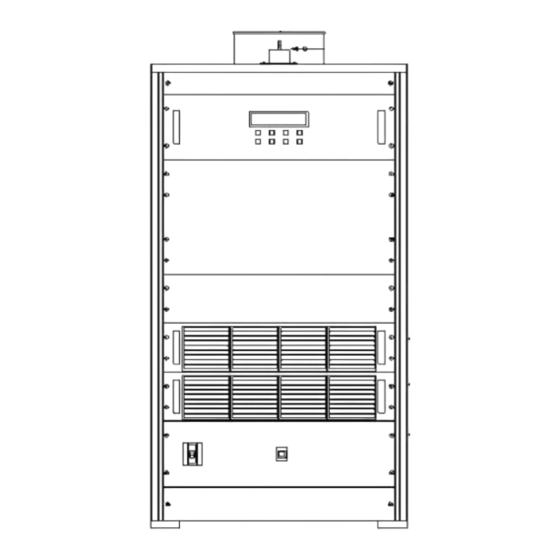
- Page 6 Section 1 – AT7200 Technical Specifications 1. Introduction The AT7200 is a 200W UHF ATSC/8VSB transmitter assembled and tested in United States by LINEAR INDUSTRIES INC. (www.linear-tv.com). Fig1.1: AT7200 Front View, cabinet wheels are optional. AT7400 Owner Manual Rev. 2.0 – October 2006-10-23...
- Page 7 2. AT7200 RF line Up: 3. AT7200 Cabinet Air Flux: 0.25m /sec. - 21ft /sec. Air Outlet Cold Air Inlet Fig. 1.4: Air flux path at AT4700 cabinet, (lateral view). Darker area denotes the internal heat source, or the RF drawers, (1) Exciter and (2) PA’s. AT7400 Owner Manual Rev.
- Page 8 UHF. Ch14 to Ch69, (4 bands). Frequency Step 1 Hz. ± 220kHz Symbol Rate 10.76 MSymbol/sec. Digital/Analog Converter 16 bit All –Digital Linear. Pre-Correction Included Pilot frequency stability overall ± 0.3 ppm. ≤0.15 dB. Peak to peak frequency response ≤15 ns.
- Page 9 5. AT4700 available models and options Models Mono-phase; 220Vac. 3-phase; 220Vac – 380Vac; 3 wires. 3-phase; 220Vac – 380Vac; 4 wires. Options: Integrated GPS receiver Adaptive digital pre-correction Dual Exciter Analog Transmission Mode Cabinet 4 wheels 6. AT7400 Typical Test Report 6.1.Out of Channel Emissions AT7400 Owner Manual Rev.
- Page 10 6.2.Frequency Response and Group Delay 6.3.Carrier Phase Noise AT7400 Owner Manual Rev. 2.0 – October 2006-10-23 Section 1 - 5/7...
- Page 11 6.4.Digital Modulation Error Rate: AT7400 Owner Manual Rev. 2.0 – October 2006-10-23 Section 1 - 6/7...
-
Page 12: Conducted Spurious Emissions
6.5.Conducted Spurious Emissions AT7400 Owner Manual Rev. 2.0 – October 2006-10-23 Section 1 - 7/7... -
Page 13: Section 2 - Master Control Unit
Section 2 – Master Control Unit Module 4459 1. General Description The main control unit, MCU, is the logical master unit acting all over the transmitter operational functions. The MCU is constantly connected and exchanging information via RS485 with the UHF power amplifiers units and the UHF exciter unit. - Page 14 2.6.Module 4459 Block Diagram Fig.2.2: – Module 4459 block diagram and PCBs displacement. AT7400 Owner Manual Rev. 2.0 – October 2006-10-23 Section 2 - 2/9...
- Page 15 2.7.Unit Control Board CIM3297 at Module 4459 This is the principal board on the MCU module. See Fig.2.5 for the PCB CIM3297 connections. The logic functions performed by the PCB CIM3297 are as follows: CI -1 CI -1 CI-3 CI-3 CI-3 +15V +15V...
-
Page 16: Digital Control
Fig.2.4: – Module 4459, CIM 3297 the transmitter main microcontroller. 2.7.1. Digital Control o The integrated circuit CI-4 (A128) is a 16 bit microcontroller, programmed on assembler language. This integrated circuit controls this module, 4459, and also the entire transmitter. This IC carries a controlled software version, and is programmed on factory. -
Page 17: Analog Readings
2.7.2. Analog Readings Information on analog format is available at the connectors P1 and P2 on the module 4459’s panel, which are routed to CON-9 at the PCB CIM3297. On P1-P2 connectors are available the following analog reading from external measurements: Fig. -
Page 18: Alarm Detection
2.7.2.1 Direct RF power, and reverse RF power. From the RF output directional coupler, module 4429. 2.7.2.2 Direct RF driver power, and reverse RF driver power. From the RF intermediate directional coupler, module 4429. 2.7.2.3 +8V, from the DC/DC converter; module 4147. 2.7.2.4 +15V, from the DC/DC converter;... -
Page 19: Rs485 Communication Bus
2.7.4. RS485 Communication bus On the PCB CIM3297, pin 1 and pin 2, at the CON-12 perform the RS485 communication link among the MCU, the UHF exciter driver drawer and the UHF power amplifier drawers. 2.7.5. Interface SNMP The interface SNMP is the PCB CIM3453. The connectors CON-4 and CON-10 located at the PCB CIM 3297 links the 2 PCBs. - Page 20 2.7.6. Displaying the Exciter and Power Amplifier Drawers Alarms Each drawer has its own local control units. The local processed data is link to the MCU via RS485 protocol. The MCU unit analyze, command actions and display at the LCD, the overall system status. Alarms from the drawers, are displayed as drawers alarms, followed by one of each signs “!”, or “#”.
- Page 21 2.7.9. Module 4459 Internal Wiring Fig. 29: - Module 4459 wiring diagram. 2.7.10. Module 4459 Schematic Diagrams: SEE ANNEX A 2.7.10.1 - PCB CIM3297 2.7.10.2 - PCB CIM3112 2.7.10.3 - PCB CIM3108 2.7.10.4 - PCB CIM3453 AT7400 Owner Manual Rev. 2.0 – October 2006-10-23 Section 2 - 9/9...
- Page 22 Section 3 – 20W UHF ATSC Exciter Unit/Drawer GAV4452 1.General Description The 20W UHF ATSC exciter drawer performs several important functions, as follows: The 8VSB modulation. Incoming SMPTE310 data stream, over an IF carrier, 21.52MHz. Insert the pre-distortion function over the modulated IF signal. Fig.3.1: Top GAV4452 front view, bottom GAV4452 rear view.
- Page 23 The modules assembled into the GAV4452 are: 01 Module 4454 - 8VSB Modulator and MASTER Clock Generator 01 Module 4453 - IF/UHF Up-Converter 01 Module 4466 - DDS 01 Module 4464 - 20W UHF / ATSC ...
- Page 24 2.GAV4452 – 30W UHF/ATSC Exciter – Block Diagram AT7400 Owner Manual Rev. 2.0 – October 2006-10-23 Section 3 - 3/39...
- Page 25 3.GAV4452 - Module 4454 – 8VSB Modulators and Master Clock 3.1. General Functional Description The module 4454 can be break down in 2 printed circuit boards. These boards are physically located as the figure below: CON-7 (WH) GROUND ? CON-5 – CIM3458 – MOD.4470 – VOLTAGE REGULATORS (BR) +5V ? CON-2 –...
- Page 26 CIP8357 CIP8355 8VSB Modulator RF UHF SMPTE 310 & Mixer & ALC -2.3dBm pre-distortion External Master Clock PLL + DDS Reference 172.16MHz 4 x VCO/off set 10MHz CIP8358 CIP8356 Sub-module 4454 Sub-module 4453 Fig.3.4: Module 4454- 8VSB Modulation and IF/UHF up-conversion structure 3.1.1.
- Page 27 3.1.1.1 PCB CIM3444 – General Functional Description The ADVANCE TV series is designed to receive as input signal, programming stream, standard SMPTE310M,with 19.39M bps, amplitude of 800 mVpp, @75Ω . The input BNC connector is located on the top cover of the transmitter rack. First the circuit to recover the clock rate used to perform the protocol interface.
- Page 28 The value for the system when working with 2 orthogonal carriers is because it is possible to implement corrections on non-linear distortions, or simply implement digital pre-distortion. The digital pre-correction is possible using LUT, (Look up Tables). This table synthesizes inverted responses regarding the RF power amplifier transfer function, reducing the IMD products.
- Page 29 3.1.3. PCB CIM3445 – Master Clock - Block Diagram 3.1.4. PCB CIM3445 – General Functional Description The 172.16MHz frequency is synthesized via a PLL, a VCO and a DDS circuit. The 10MHz reference is one out of the two inputs of the phase comparator. This signal comes to CIP8358 via a SMB connector, CON-2. The second one is also a 10MHz generated by the DDS circuit out from the free running 172.16MHz oscillator.
- Page 30 3.2.1. Module 4453 - External Connections CON-7 CON-7 CON-2 CON-2 (WH) GROUND ? CON- 5 – CIM345 8 – MOD.4470 – VOLTAGE REGUL ATORS (WH) GROUND ? CON- 5 – CIM345 8 – MOD.4470 – VOLTAGE REGUL ATORS (OR) +3.3V ? CON- 8– CIM345 8 – MOD.4470 – VOLTAGE REGUL ATORS (OR) +3.3V ? CON- 8–...
- Page 31 3.2.2. PCB CIM3443 – Local Oscillator The local oscillator is designed based on a PLL circuit. This oscillator is able to synthesize frequencies within the band from 450MHz up to 900MHz. To guarantee a high quality signal generation out from the local oscillator, 4 VCO’s (voltage controlled oscillator) were implemented with a shift frequency range of 125MHz each.
- Page 32 3.3.1. PCB CIM3442 – UHF Mixer – Block Diagram AT7400 Owner Manual Rev. 2.0 – October 2006-10-23 Section 3 - 11/39...
- Page 33 3.3.2. PCB CIM3442 – UHF Mixer – Test Points Diagram AT7400 Owner Manual Rev. 2.0 – October 2006-10-23 Section 3 - 12/39...
- Page 34 3.3.3. PCB CIM3442 – UHF Mixer – Adjustment Procedures The mixer-ALC circuitries have 2 types of adjustments. The first one is a DC level that polarizes each branch of the input of the complex mixer. Each one of the DC levels must be adjusted seeking for the max rejection on the un-desired vestigial side band, in conjunction with the LO rejection as well.
- Page 35 3.5. Module 4466 – External Connections AT7400 Owner Manual Rev. 2.0 – October 2006-10-23 Section 3 - 14/39...
- Page 36 3.6. Module 4464 – 20W UHF ATSC Power Amplifier The RF/UHF signal, already set to the assigned channel, is than power amplified up to 20W. The RF amplifier is type class AB. LDMOS transistors are also used on this amplification stage. Fig.:3.2; illustrates the RF chain of the module 4464.
-
Page 37: General Functional Description
3.1.3.1 General Functional Description The PCB CIM 3390 delivers is the output nominal ATSC UHF 20W output power for the module 4455 – intermediate directional coupler. Despite the amplifier being designed as a broadband amplifier, due optimization reasons, the amplifier is built in 4 frequency operational bands, as follows: channel 14 to 25 (B1) - channel 26 to 38 (B2) - channel 39 to 53 (B3) - channel 54 to 69 (B4) Despite the different bands, the PCB remains the same, as indicated on the table below: 20W UHF / ATSC EXCITER - MODULE 4464... - Page 38 3.9.1. Module 4464 – Technical Specifications CHARACTERISTIC SPECIFICATION SMPTE310M INPUT FREQUENCY 470 - 862MHz IMPEDANCE 75 Ohms CONNECTOR BNC FEMALE ³ 22dB RETURN LOSS RF OUTPUT GAIN FROM 45 TO 48dB ATSC UNTIL 20W AVERAGE POWER £ -60dB HARMONICS SPURIOUS <...
- Page 39 3.9.2. Module 4464 – PCB CIM3446 – 32dB Gain Driver 0.5w Amplifier The PCB CIM 3446 is the driver amplifier for the 20W final amplifier. This circuit is 2 parallels cells, type class A polarization, 90 degree out of phase, able to delivery up to 1W of power usable for DTV/ATSC standard over the 470MHz –...
- Page 40 3.9.3. Module 4464 – CIM 3446 – Technical Specifications AT7400 Owner Manual Rev. 2.0 – October 2006-10-23 Section 3 - 19/39...
- Page 41 +5V / 1A VOLTAGE ALARM +12V / 1A VOLTAGE SUPPLY 30dB / 50W SUPPLY +32V / 2A VOLTAGE ATTENUATO SUPPLY 8359 LINEAR +32V TPO - 1 VGS T2 (RD) TPO- 1 CON - 1 VGS ADJ CON - 2 (GY)
- Page 42 3.9.4.1.1. Transistor T2 1 – Turn TPO-1’s knob all way counter clock wise, no T2-ID will be present. 2 – Connect the multi-meter over the terminals of R13, the T2-drain resistor. 3 – Slowly start to turn TPO-1 knob clock wise up to the point that T2 starts to conduct, meaning few mili-volts will be read at the multi-meter.
- Page 43 According with the Fig. 3.2: block diagram: AT7400 Owner Manual Rev. 2.0 – October 2006-10-23 Section 3 - 22/39...
- Page 44 3.9.5.1 RF Hybrid Input This hybrid equally splits the incoming RF signal, keeping the input impedance at 50Ω level on an eventual amplification cell malfunction. This hybrid is built out of 2 coupled transmission lines. In one end of the first transmission line is connected the RF input signal, and on the other end a 50Ω/10W (R1 parallel with R2) resistive termination.
-
Page 45: Temperature Alarm
3.9.5.3 UHF 12.5W Driver Amplifier – Cell B, Transistor 2 On this cell, the trim-pot TPO-3 at the same time adjusts the VGS2 voltage for T2, and the drained current ID. The trimmers C35, C39 and C43, tunes and adjusts the input impedance. A combination among the trimmers’ physical position and transmission lines’... -
Page 46: Specification
3.9.6. Module 4464 – PCB CIM3440 – Technical Specifications FEATURE SPECIFICATION INPUT FREQUENCY 470 - 862MHz IMPEDANCE 50 Ohms ³ 22dB RETURN LOSS OUTPUT GAIN 13 TO 16dB RF POWER UNTIL 20WRMS £ -60dB HARMONICS SPURIOUS < -54dB EMISSION INTERMODULATION <... - Page 47 3.9.7.1 Drain Current ID, Adjustment Turn the unit ON and wait 3 minutes for thermal stability. Use a good quality multi-meter able to read mVdc, avoid to used auto-range multi-meters. 3.9.7.1.1. Transistor T1 1 - Set the trim-pot TPO-1 all way counterclockwise. On this condition no current flow over the transistor. 2 –...
- Page 48 NETWORK ANALYZER NETWORK ANALYZER 30dB / 50W 30dB / 50W ATTENUATOR ATTENUATOR TPO-1 TPO-1 TPO-1 VG S ADJ VG S ADJ VG S ADJ CON -2 CON -2 CON -2 CI - 7 CI - 7 CI - 7 +32V +32V +32V CI - 3...
- Page 49 Fig. 3.13: Module 4456 – 60A multiple power supply The module 4456 generates the following voltage values for this drawer internal use only: Voltage Current +32V Fixed +32V ON/OFF according to command. +15V Direct +15V -15V 200 mA +2.5V Table 2 - Module 4456: Listing of Voltage and current, per each power supply. The multiple power supply module 4456 is composed by the following PCB’s: AT7400 Owner Manual Rev.
- Page 50 Fig. 3.13: Module 4456 - Circuit functions: electrical schematic diagram, (CIM), and printed circuit board, (CIP). AT7400 Owner Manual Rev. 2.0 – October 2006-10-23 Section 3 - 29/39...
- Page 51 Module 4456 – Block Diagram 3.10.1. AT7400 Owner Manual Rev. 2.0 – October 2006-10-23 Section 3 - 30/39...
Need help?
Do you have a question about the ADVANCED AT7200 and is the answer not in the manual?
Questions and answers