
Subscribe to Our Youtube Channel
Related Manuals for Panasonic DMR-E85HEB


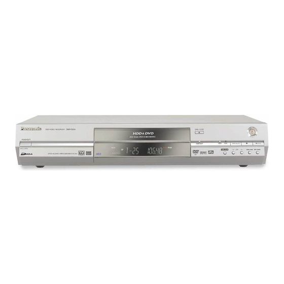
Summary of Contents for Panasonic DMR-E85HEB
- Page 1 ORDER NO.DSD0403005C2 DVD Video Recorder DMR-E85HEB / DMR-E85HEG Colour (K).......Black Type (S).......Silver Type SPECIFICATIONS...
- Page 2 2004 Matsushita Electric Industrial CO., Ltd. All rights reserved. Unauthorized copying and distribution is a violation of law. 1. Safety precautions 1.1. General guidelines 1. When servicing, observe the original lead dress. If a short circuit is found, replace all parts which have been overheated or...
- Page 3 damaged by the short circuit. 2. After servicing, see to it that all the protective devices such as insulation barriers, insulation papers shields are properly installed. 3. After servicing, make the following leakage current checks to prevent the customer from being exposed to shock hazards. 1.1.1.
- Page 4 6. The potential at any point should not exceed 0.75 volts RMS. A leakage current tester (Simpson Model 229 or equivalent) may be used to make the hot checks, leakage current must not exceed 1/2 milliampere. In case a measurement isoutside of the limits specified, there is a possibility of a shock hazard, and the equipment should be repaired and rechecked before it is returned to the customer.
- Page 5 comparableconductive material). 7. Immediately before removing the protective material from the leads of a replacement ES device, touch the protective material to the chassis or circuit assembly into which the device will be installed. Caution Be sure no power is applied to the chassis or circuit, and observe all other safety precautions.
- Page 6 4.1. About lead free solder (PbF) Distinction of PbF P.C.B.: P.C.B.s (manufactured) using lead free solder will have a PbF stamp on the P.C.B. Caution: - Pb free solder has a higher melting point than standard solder; Typically the melting point is 50 - 70°F (30 - 40°C) higher. Please use a high temperature soldering iron.
- Page 7 direction of Arrow. 6. Put the Upper Base Unit so that the Opener Roller is inserted into the groove. 7. Check center of Opener Roller is seen through the Opener position Checking Hole, and tighten 4 screws. 7. Service Explorer Confirm “RAM-Drive Last Error”...
- Page 8 *After finishing display “(7). Factor of Drive Error occurring”, press [0] [2] ~[9] [9] keys of the Remote Controller so that 99 memories can be displayed as maximum. 2. Press [4] [2] keys of remote controller. Example of FL Display: (1) Error Number is displayed for 5 seconds.
- Page 9 FL Display (Disc Disc Maker Country Maker's ID) Panasonic Japan Pioneer Japan Mitsubishi Chemical Japan Corporation Japan Maxell Japan MITUI CHEMICALS Japan Victor JVC Japan TAIYOYUDEN Taiyo yuden Japan Giga Storage Taiwan PRODISC Prodisc Taiwan PRINCO PRINCO Taiwan RITEK RITEK...
- Page 10 FL Display Disc Type DVD-ROM/Video Audio-CD 2.6GB DVD-RAM 4.7GB DVD-RAM DVD-R Error Occurring Disc State 8. Self-Diagnosis and Special Mode Setting 8.1. Self-Diagnosis Functions Self-Diagnosis Function provides information for errors to service personnel by “Self-Diagnosis Display” when any error has occurred. U14, H** and F** are stored in memory and held.
- Page 11 Error Diagnosis contents Description Monitor FL display Display Code Remote control code Display appears when main unit No display error and remote controller codes are not matched. “*” is remote controller code of the main Display for 5 seconds. Abnormal inner Display appears when the drive No display temperature detected...
- Page 12 Error Diagnosis contents Description Monitor FL display Display Code Unsupported disc error *An unsupported format disc was “This disc is UNSUPPORT played, although the drive starts incompatible.” normally. *The data format is not Display for 5 seconds. supported, although the media type is supported.
- Page 13 Item FL display Key operation Mode name Description Front Key TEST Mode *All the main unit's parameters Press [SKIP (REV)], (include tuner) are initialized. SLIP] and [OPEN keys simultaneously five seconds when is off. Service Mode Setting every kind of modes for When the power servicing.
- Page 14 Item FL display Key operation Mode name Description Front Key Aging Perform sequence of modes as * Display following the then When the power Aging Description shown below mode. press [CH DOWN], continually. SLIP] and [OPEN simultaneously for five seconds and than 10 seconds.
- Page 15 Item FL display Key operation Mode name Description Front Key Progressive The progressive setting is The display before When the power initialization initialized to Interlace. execution leaves. mode), press [STOP] [TIME SLIP] simultaneously for seconds. Aging Contents (Example): 8.3. Service Modes Service mode setting: While the power is off, press TIME SLIP, STOP and OPEN / CLOSE simultaneously for five seconds.
- Page 16 Item FL display Key operation Mode name Description (Remote controller ROM Version Region code, MAIN firm version, Press [0] [2] in service Display TIMER firm version and DRIVE mode firmware versions are displayed on FL for five seconds per each version in order, but ROM version will be left displayed.
- Page 17 Item FL display Key operation Mode name Description (Remote controller White Picture White picture is output as *Initial mode is “Interlace”. Press [1] [1] in service Output component Output from AV mode. Decoder. *White picture Switch Interlace/ Press [1] [4] in White (Saturation rate : 100%) Progressive Picture Output mode.
- Page 18 Item FL display Key operation Mode name Description (Remote controller RTSC Return in XP AV1 input signal is encoded (XP), Initial mode: EE2/ Interlace/ Press [1] [3] in service decoded (XP) and output XP/ Audio 48kHz mode. decoded signal to external (A &...
- Page 19 Item FL display Key operation Mode name Description (Remote controller HDD READ Perform a complete read When the HDD is OK Press [3] [1] in the inspection inspection of the HDD. mode. *When canceling checking mode while executing, do "forced If the HDD is defective power-off".
- Page 20 Item FL display Key operation Mode name Description (Remote controller RAM Drive Last RAM Drive error code display. 1. Error Number is Press [4] [2] in service Error displayed for 5 seconds. mode. *For details about the drive error code, refer to the Service Manual Then press [0] [1] for the specific RAM Drive.
- Page 21 Item FL display Key operation Mode name Description (Remote controller Delete the Last Delete the Last Drive Error Press [9] [6] in service Drive Error information stored on the DVD mode. RAM-Drive. Turn on all FL/ All segments of FL and all LEDs All segments are turned Press [5] [1] in service LEDs...
- Page 22 Item FL display Key operation Mode name Description (Remote controller Display the Error Display the Error History stored Display reason of error for Press [6] [5] in service History on the unit. 5 seconds. mode. Then press [0] [1] the past 19 error are displayed.
- Page 23 Item FL display Key operation Mode name Description (Remote controller P50 (H) Output Timer Microprocessor IC7501-22 Press [8] [4] in service output High signal for AV1-pin 10 mode. passing through inverter (approx. 0V DC at AV1-pin 10). When OK. When NG. P50 (L) Output Timer Microprocessor IC7501-22 Press [8] [5] in service...
- Page 24 The following chart is the procedure for disassembling the casing and inside parts for internal inspection when carrying out the servicing. To assemble the unit, reverse the steps shown in the chart below. 9.2. P.C.B. Positions 9.3. Top Case 1. Remove the 2 screws (A) and 3 screws (B). 2.
- Page 25 9.4. Digital P.C.B. 1. Remove the FFC and a Screw. 2. Unlock a Rocking Spacer. 3. Lift up Digital P.C.B. slightly so to disconnect Connector to remove Digital P.C.B. CAUTION: When replacing Digital P.C.B., pay attention as below.
- Page 26 9.5. Front Panel 1. Remove 3 tabs (A) and 2 tabs (B) in this order. (The tab (A) and (B) should be removed at the same time, respectively.) 2. Move the front panel to front side straight and slowly so to remove it with Connector.
- Page 27 9.6. Front (R) P.C.B. 1. Remove 6 screws and Front Angle. 9.7. HDD 1. Remove 3 Screws (A) and 2 connectors. 2. Slide and lift up HDD Holder in the direction of the arrows so to unlock 3 locking tabs.
- Page 28 3. Lift up HDD with super sheet vertically and remove super sheet. Handling of HDD The following precautions should be taken when handling HDD. 1. Never give an impact to HDD. (Even a drop from 1cm height can be a cause of HDD failure.
- Page 29 9.8. HDD Bracket 1. Remove 4 screws (B) and HDD Bracket with 2 Insulation Sheets. 9.9. DVD-RAM Drive 1. Remove 3 Screws. 2. Pull out DVD-RAM Drive vertically so to remove it with Connector. 9.10. Rear Panel 1. Remove the 12 screws (A) and screw (B). 2.
- Page 30 9.10.1. Only Fan Motor 1. Remove the 2 screws. 2. Remove Fan Connector to remove Fan Motor. 9.11. Main P.C.B. 1. Remove the 7 screws (A), Connector (A) and Fan Connector.
- Page 31 2. Remove a Screw (B) and lift up Front Jack portion of Main P.C.B. slightly so to unlock Tab to remove Main P.C.B.. 9.12. Power P.C.B. 1. Lift up Power P.C.B. a little so to unlock 2 Tabs and slide Power P.C.B.
- Page 32 9.13. The Scart P.C.B. 1. Pull out the Scart P.C.B. in the direction of the arrow. Note: At first disconnect the connector on one side, and pull out the Scart P.C.B. 9.14. VIF Decoder P.C.B. and Nicam Decoder P.C.B. 1. Remove the solders. 2.
- Page 33 10. Service Fixture and Tools Part Number Description Compatibility RFKZ0125 Extension FFC (Digital P.C.B. - DVD-RAM Drive / 40 Pin) Same as E50 series RFKZ0168 Extension Cable (Main P.C.B. - Fan / 3 Pin) Same as E50 series RFKZ0169 Extension Cable (Power P.C.B. - HDD / 4 Pin) Same as E100H series RFKZ0197 Extension Cable (Main P.C.B.
- Page 34 11. Service Positions Note: For description of the disassembling procedure, see the section 9. 11.1. Checking and Repairing of Power P.C.B.
- Page 35 11.2. Checking and Repairing of Main P.C.B.
- Page 36 11.3. Checking and Repairing of Digital P.C.B.
- Page 37 11.4. Checking and Repairing of DVD-RAM Drive...
- Page 38 11.5. Checking and Repairing of HDD...
- Page 39 12. Adjustment Procedures 12.1. After replacing the RAM Drive with new one 12.2. When the unit does not operate normally after replacing the Timer Microprocessor with new one in order to transmit the Step Operation Descriptions While power is ON, short IC7508-4 pin (RESET) and “RESET (L)”...
- Page 40 Turn on the power, and confirm items pointed out. Items pointed out should reappear. Insert RAM disc. The Panasonic RAM disc should be recognized. Enter the EE (TU IN / AV IN - AV OUT) mode. No abnormality should be seen in the picture, sound or operation.
-
Page 41: Table Of Contents
14. Voltage and Waveform Chart Note) - Indicated voltage values are the standard values for the unit measured by the DC electronic circuit tester (high-impedance) with the chassis taken as standard. Therefore, there may exist some errors in the voltage values, depending on the internal impedance of the DC circuit tester. - Page 42 INITIAL/LOGO ABBREVIATIONS A0~UP ADDRESS ACLK AUDIO CLOCK AD0~UP ADDRESS BUS ADATA AUDIO PES PACKET DATA ADDRESS LATCH ENABLE AMUTE AUDIO MUTE AREQ AUDIO PES PACKET REQUEST AUDIO RF SERVO AMP INVERTED INPUT SERVO AMPOUTPUT ASYNC AUDIO WORD DISTINCTION SYNC BIT CLOCK (PCM) BCKIN BIT CLOCK INPUT BLACK DROP OUT...
- Page 43 INITIAL/LOGO ABBREVIATIONS DACCK D/A CONVERTER CLOCK DEEMP DEEMPHASIS BIT ON/OFF DEMPH DEEMPHASIS SWITCHING DIG0~UP FL DIGIT OUTPUT DATA INPUT DMSRCK DM SERIAL DATA READ CLOCK DMUTE DIGITAL MUTE CONTROL DROP OUT DOUT0~UP DATAOUTPUT DATA SLICE RF (BIAS) DRPOUT DROP OUT SIGNAL DREQ DATA REQUEST DRESP...
- Page 44 INITIAL/LOGO ABBREVIATIONS IECOUT IEC958 FORMAT DATA OUTPUT IPFRAG INTERPOLATION FLAG IREF I (CURRENT) REFERENCE ISEL INTERFACE MODE SELECT LDON LASER DIODE CONTROL LASER POWER CONTROL LRCK L CH/R CH DISTINCTION CLOCK MA0~UP MEMORY ADDRESS MEMORY CLOCK MCKI MEMORY CLOCK INPUT MCLK MEMORY SERIAL COMMAND CLOCK...
- Page 45 INITIAL/LOGO ABBREVIATIONS READ ENABLE RFENV RF ENVELOPE RF PHASE DIFFERENCE OUTPUT (CD-ROM) REGISTER SELECT RSEL RF POLARITY SELECT RESET RESERVE SBI0, 1 SERIAL DATA INPUT SBO0 SERIAL DATA OUTPUT SBT0, 1 SERIAL CLOCK SERIAL DATA CLOCK SCKR AUDIO SERIAL CLOCK RECEIVER SERIAL CLOCK SCLK...
- Page 46 SYSTEM CLOCK INITIAL/LOGO ABBREVIATIONS TRACKING ERROR TIBAL BALANCE CONTROL BALANCE OUTPUT 1 BALANCE INPUT BALANCE INPUT BALANCE OUTPUT 2 TPSN OP AMP INPUT TPSO OP AMP OUTPUT TPSP OP AMP INVERTED INPUT TRCRS TRACK CROSSSIGNAL TRON TRACKING ON TRSON TRAVERSE SERVO ON INITIAL/LOGO ABBREVIATIONS VBLANK...
- Page 47 INITIAL/LOGO ABBREVIATIONS X' TAL XALE X ADDRESS LATCH ENABLE XAREQ X AUDIO DATA REQUEST XCDROM X CD ROM CHIP SELECT X CHIP SELECT XCSYNC X COMPOSITE SYNC X DATA STROBE XHSYNCO X HORIZONTAL SYNC OUTPUT XHINT XH INTERRUPTREQUEST X' TAL OSCILLATOR INPUT XINT X INTERRUPT X MEMORY WRITE ENABLE...
-
Page 48: Power P.c.b
17.11. AV Decoder/Main CPU Section (Digital P.C.B. (4/5)) Schematic Diagram (MC) 17.12. Audio I/O Section (Digital P.C.B. (5/5)) Schematic Diagram (AI) 17.13. VIF Decoder Schematic Diagram (For DMR-E85HEB) 17.14. VIF Decoder Schematic Diagram (For DMR-E85HEG) 17.15. Nicam Decoder Schematic Diagram 17.16. -
Page 49: Nicam Decoder P.c.b
18.3.2. Digital P.C.B. (Foil Side) 18.3.3. Digital P.C.B. Address Information 18.4. VIF Decoder P.C.B. (For DMR-E85HEB) 18.5. VIF Decoder P.C.B. (For DMR-E85HEG) 18.6. Nicam Decoder P.C.B. 18.7. Scart P.C.B. 18.7.1. Scart P.C.B. (Section 1/2) 18.7.2. Scart P.C.B. (Section 2/2) 18.8. Front (R) P.C.B. - Page 50 19.2. Casing Parts & Mechanism Section 2...
- Page 51 19.3. Packing & Accessories Section...
- Page 52 20. Replacement Parts List Notes: *Important safety notice: Components identified by mark have special characteristics important for safety. Furthermore, special parts which have purposes of fire-retardant (resistors), high-quality sound (capacitors), low-noise (resistors), etc. are used. When replacing any of components, be sure to use only manufactures specified parts shown in the parts list.
- Page 53 *Capacity values are in microfarads ( F) unless specified otherwise, P=Pico-farads (pF), F= Farads (F). *Resistance values are in ohms, unless specified otherwise, 1K=1,000 (OHM), 1M=1,000k (OHM). *The marking (RTL) indicates the retention time is limited for this item. After the discontinuation of this assembly in production, it will no longer be available.
- Page 54 Ref. No. Part No. Part Name & Description Remarks 12-12 RGK1811-S FL ORNAMENT EB,EG-S 12-13 VGB0560 PANASONIC BADGE 12-14 RHD26016 SCREW 12-15 RMX0299 DAMPER SHEET 12-16 RMR1637-W REFLECTOR DVD 12-17 RMR1638-W REFLECTOR HDD 12-18 XTN2+6G SCREW 12-19 RMR1655-W REFLECTOR COVER REP3713B FRONT(R) P.C.B.
- Page 55 Ref. No. Part No. Part Name & Description Remarks A6-6 RQCA1119 HDD CAUTION SHEET A6-6 RQCA1222 HDD CAUTION SHEET A6-7 RQCA1231 PAL PROGRESSIVE SHEET A6-8 RQCA1244 DVD-R REC SHEET A6-8 RQCA1245 DVD-R REC SHEET A6-9 RQCA1195 SETUP GUIDE RPQ1594 RPG7129 PACKING CASE EG-S RPG7130...
- Page 56 C3030,31 ECJ1VB1H103K 50V 0.01U...
- Page 57 Ref. No. Part No. Part Name & Description Remarks C3032 ECEA0JKS331 6.3V 330U C3033 ECEA1CKS220 16V 22U C3034 ECEA0JKS331 6.3V 330U C3035 ECEA1CKS220 16V 22U C3036 ECEA0JKS331 6.3V 330U C3037 ECEA1CKS220 16V 22U C3038 ECJ1XB1C104K 16V 0.1U ECJ1VB1C104K C3039 ECJ1VB0J105K 6.3V 1U C3040 ECJ1VB1H103K...
- Page 58 Ref. No. Part No. Part Name & Description Remarks C4056 F2A0J471A247 6.3V 470U C4057 ECJ2VC1H680J 50V 68P C4059 ECQV1H104JL 50V 0.1U C4060 ECJ2VC1H680J 50V 68P C4061 ECJ1VF1C104Z 16V 0.1U C4062 ECA1AM221 10V 220U C4063,64 F2A1C4700011 16V 47U C4065 ECJ1VF1C104Z 16V 0.1U C4067 F2A0J470A179 6.3V 47U...
- Page 59 Ref. No. Part No. Part Name & Description Remarks C7526 ECJ1XB1C104K 16V 0.1U ECJ1VB1C104K C7527 F2A0J470A012 6.3V 47U C7528 ECJ1VF1C104Z 16V 0.1U C7529 F2A0J470A012 6.3V 47U C7546 ECJ1XB1C104K 16V 0.1U ECJ1VB1C104K C7550 ECJ1VB1H103K 50V 0.01U C7551 ECA1HHG100 50V 10U C7552 ECJ1VF1H104Z 50V 0.1U C7555...
- Page 60 Ref. No. Part No. Part Name & Description Remarks D1501 MA165TA5 DIODE MA2C16500E D4001 MA165TA5 DIODE MA2C16500E D4005,06 MA3Z142D0RG DIODE D7401 MA165TA5 DIODE MA2C16500E D7402 MA4300N-M DIODE MAZ4300NM D7403 MA165TA5 DIODE MA2C16500E D7501 MAZ4240NMF DIODE D7502 B0AAGM000003 DIODE B0AAGM000007 D7504,05 MA2C18500E DIODE D7506...
- Page 61 JK7501 K1U415B00001 JACK,AV3...
- Page 62 Ref. No. Part No. Part Name & Description Remarks K7508 ERJ3GEY0R00V 1/10W 0 K7510,11 ERJ3GEY0R00V 1/10W 0 K7514,15 ERJ3GEY0R00V 1/10W 0 L1501 G0A220G00018 COIL 22UH L4002 ELESE220KA COIL 22UH L7401 G0A220G00018 COIL 22UH L7402 VLQ0599J270 COIL 27UH G0C270JA0026 EB L7403 G0C2R2JA0019 COIL 2.2UH LB1501...
- Page 63 Ref. No. Part No. Part Name & Description Remarks Q7512 2SD0874A0L TRANSISTOR Q7517 2SD0601A TRANSISTOR Q7518 2SD1819AWL TRANSISTOR Q7519 2SD0601A TRANSISTOR QR3002,03 UN5212TX TRANSISTOR UNR521200L QR4002-05 UN5211 TRANSISTOR UNR5211 QR4012 UN5113TW TRANSISTOR QR7401-03 UN5213TX TRANSISTOR UNR521300L QR7404 UNR511400L TRANSISTOR QR7405 UN5213TX TRANSISTOR UNR521300L...
- Page 64 Ref. No. Part No. Part Name & Description Remarks R4012 ERJ3GEYJ333V 1/10W 33K D0GB333JA002 R4013 ERJ6GEYJ102V 1/8W 1K R4014 ERJ3GEYJ103V 1/10W 10K D0GB103JA002 R4015 ERJ6GEYJ102V 1/8W 1K R4017 ERJ3GEYJ103V 1/10W 10K D0GB103JA002 R4018 ERJ3GEY0R00V 1/10W 0 R4019,20 ERJ3GEYJ473V 1/10W 47K D0GB473JA002 R4021,22 ERJ3GEYJ823V...
- Page 65 Ref. No. Part No. Part Name & Description Remarks R7432 ERJ3GEYJ223V 1/10W 22K D0GB223JA002 R7433 ERJ3GEYJ102V 1/10W 1K R7434 ERJ3GEYJ333V 1/10W 33K D0GB333JA002 R7435 ERJ3GEYJ223V 1/10W 22K D0GB223JA002 R7436,37 ERJ3GEYJ221V 1/10W 220 R7438-42 ERJ3GEYJ220V 1/10W 22 R7443 ERJ3GEYJ101 1/10W 100 D0GB101JA002 EG R7444 ERJ3GEY0R00V...
- Page 66 Ref. No. Part No. Part Name & Description Remarks R7595,96 ERJ3GEYJ473V 1/10W 47K D0GB473JA002 R7597 ERJ3GEYD153V 1/10W 15K D0HB153ZA002 R7598 ERJ3GEYJ181V 1/10W 180 R7599 ERJ3GEYJ223V 1/10W 22K D0GB223JA002 R7600,01 ERJ3GEYJ103V 1/10W 10K D0GB103JA002 R7602 ERJ3GEYJ821V 1/10W 820 R7603 ERJ3GEYJ183V 1/10W 18K D0GB183JA002 R7604-06 ERJ3EKF75R0...
- Page 67 Ref. No. Part No. Part Name & Description Remarks C0701 ECEA1HKS010 50V 1U C0701 ECJ1VF1H103Z 50V 0.01U C0702 ECUV1H151JCG 50V 150P ECJ2VC1H151J EG C0702 ERJ3GEYJ102V 1/10W 1K C0703 ECEA1HKS010 50V 1U C0703 ECJ1VF1H103Z 50V 0.01U C0704 ECJ1VB1E683K 25V 0.0683U C0704 ECUX1H270JCX 50V 27P ECJ2VC1H270J EG...
- Page 68 Ref. No. Part No. Part Name & Description Remarks IC0701 C1AB00001924 K0709 ERJ3GEY0R00V 1/10W 0 L0701 ELJNAR27JF COIL 27UH L0702 ELJNAR18JF COIL 18UH L0703 ELJNA3R3JF COIL 3.3UH L0703 ELJNAR68JF COIL 68UH L0704-07 ELJFA151KF COIL 150UH PK0701 VJR0826E009W CONNECTOR(9P) K1MR09A00028 PP0701 VJP3589E004B CONNECTOR(4P) K1KA04B00135...
- Page 69 Ref. No. Part No. Part Name & Description Remarks R0742 ERJ6GEYJ471V 1/8W 470 R0743 ERJ6GEYJ820V 1/8W 82 R0747,48 ERJ3GEYJ271V 1/10W 270 R0750 ERJ6GEYG562 1/8W 5.6K R0755,56 ERJ6GEYJ101V 1/8W 100 R0757 ERJ3GEYJ752V 1/10W 7.5K VR0701 EVNCYAA03B14 V.R. ERJ6GEY0R00V 1/8W 0 ERJ8GEY0R00V 1/4W 0 ERJ6GEY0R00V 1/8W 0...
- Page 70 C7323 ECJ1VC1H102J 50V 1000P...
- Page 71 Ref. No. Part No. Part Name & Description Remarks C7324 ECJ1VF1C104Z 16V 0.1U C7329 ERJ3GEY0R00V 1/10W 0 C7330 ERJ3GEYJ822V 1/10W 8.2K D0GB822JA002 C7332 ECJ1VF1C104Z 16V 0.1U C7333 ECJ1XB1C104K 16V 0.1U ECJ1VB1C104K C7334 ECEA1HKS2R2 50V 2.2U C7335 ECJ1VF1C104Z 16V 0.1U IC7301 TDA9874AH C1AB00001404 IC7302...
- Page 72 C3933 ECA1CAK101XB 16V 100U...
- Page 73 Ref. No. Part No. Part Name & Description Remarks C3934 ECJ1VB1H103K 50V 0.01U C3935 ECA1CAK101XB 16V 100U C3938 ECJ1VF1C104Z 16V 0.1U C3939 ECJ1VB1H103K 50V 0.01U C3951,52 ECJ1VC1H470J 50V 47P C3953,54 ECJ1VC1H471J 50V 470P C3955,56 ECJ1VC1H101J 50V 100P C3957,58 ECJ1VC1H471J 50V 470P C3959,60 ECJ1VC1H470J 50V 47P...
- Page 74 Ref. No. Part No. Part Name & Description Remarks R3922,23 ERJ6GEYJ471V 1/8W 470 R3924 ERDS2FJ471 1/4W 470 R3925-28 ERJ6ENF75R0 1/8W 75 R3929,30 ERJ6GEYJ471V 1/8W 470 R3931-33 ERJ3RED750V 1/16W 75 R3934,35 ERJ6ENF75R0 1/8W 75 R3962 ERJ3GEYJ103V 1/10W 10K D0GB103JA002 R3967 ERJ3GEYJ152V 1/10W 1.5K R3968 ERJ3GEYJ680...
- Page 75 C4414,15 ECJ0EF1C104Z 16V 0.1U...
- Page 76 Ref. No. Part No. Part Name & Description Remarks C4416 F2H0J331A016 6.3V 330U C4417 ECJ0EF1C104Z 16V 0.1U C4418 EEEHB0J101P 6.3V 100P C4421-26 ECJ0EB1E102K 25V 1000P C4427 EEEHB0J470R 6.3V 47P C4428 ECJ0EF1C104Z 16V 0.1U C4429 ECJ0EB1A104K 10V 0.1U C4430 ECST1AY106R 10V 10U C4431,32 ECJ0EF1C104Z 16V 0.1U...
- Page 77 Ref. No. Part No. Part Name & Description Remarks IC6001 MN2DS0011-HR IC6002 C0EBE0000130 IC6003 C3CBLD000091 IC6004 74LVC244APWL C0JBAZ001466 IC6005,06 C3ABRG000036 IC6701 C1ZBZ0002433 IC6703 REP3712H DIGITAL P.C.B. IC6703 RFKBE85HEB DIGITAL P.C.B. IC50001,02 C3ABPG000133 LB3404,05 J0JHC0000032 COIL LB3408,09 J0JHC0000032 COIL LB4401-04 J0JGC0000020 COIL LB4405 J0JHC0000032...
- Page 78 Ref. No. Part No. Part Name & Description Remarks R3454 ERJ2GEJ390X 1/16W 39 ERJ2RMJ390X R3455 ERJ2GEJ220X 1/16W 22 ERJ2RMJ220X R3456 ERJ2GEJ470 1/16W 47 R3457 ERJ2GE0R00X 1/16W 0 R3458 ERJ2GEJ220X 1/16W 22 ERJ2RMJ220X R3460-62 ERJ2GEJ470 1/16W 47 R3463,64 ERJ2GE0R00X 1/16W 0 R3472,73 ERJ2GEJ220X 1/16W 22...
- Page 79 Ref. No. Part No. Part Name & Description Remarks R6027 ERJ2GE0R00X 1/16W 0 R6028 ERJ2GEJ470 1/16W 47 R6029 ERJ2GEJ103 1/16W 10K R6031 ERJ2GEJ470 1/16W 47 R6035 ERJ2GEJ470 1/16W 47 R6036 ERJ2GEJ332X 1/16W 3.3K ERJ2RMJ332X R6037 ERJ2GEJ333X 1/16W 33K ERJ2RMJ333X R6039 ERJ2GEJ103 1/16W 10K R6040...
- Page 80 Ref. No. Part No. Part Name & Description Remarks R50028 ERJ2GEJ330X 1/16W 33 R50029 ERJ2GEJ102X 1/16W 1K ERJ2RMJ102X R50030 ERJ3RED220 1/16W 22 R50031 ERJ3RBD151 1/16W 150 R50032 ERJ2GEJ330X 1/16W 33 R50033 ERJ2GEJ102X 1/16W 1K ERJ2RMJ102X R50034,35 ERJ3RED160V 1/16W 16 R50036-38 ERJ2GEJ470 1/16W 47 R50039...
- Page 82 Ref. No. Part No. Part Name & Description Remarks C001 ECKENA102ME 1000P C002 ECQU2A104ML 0.1U C003 ECQU2A334ML 0.33 C006 ECKENA102ME 1000P C008 KH102M 1000P C009 KMM2W470JZ 450V 47 C010 RR3DD331K 2KV 330P C011 ECKENA102ME 1000P C012 MBC471J5 50V 470P C013 KY1H220 50V 22 C014...
- Page 83 D114 GPP20J DIODE...
- Page 84 Ref. No. Part No. Part Name & Description Remarks D120 MA2J11100L DIODE F001 19181-2A FUSE F101 SBM40 FUSE F102 SBM32 FUSE F103 SBM25 FUSE IC001 STRG6353 IC101 TL431AI IC102 LM2904DR IC105 BD4746G IC106 SI3120J IP101 ICPN10 IC PROTECTOR L002 ELF15N005A COIL L004 ELESN150KA...
- Page 85 Ref. No. Part No. Part Name & Description Remarks R001 ERDS1FJ105 0.5W 1M R002 CR10J681 0.1W 680 R003 ERX1SZGR47 1W 0.47 R005 ERDS2FJ224 1/4W 220K R006 ER0S2TKF2373 0.25W 237K R007 CR10F1272 0.1W 12.7K R008 CR10J562 0.1W 5.6K R009 ERDS2FJ224 1/4W 220K R010 ER0S2TKF2373 0.25W 237K...
- Page 86 Ref. No. Part No. Part Name & Description Remarks R172 ERJ6GEYJ101V 1/8W 100 R173 CR10J224 0.1W 220K R174 CR10J471 0.1W 470 R175 CR10J472 0.1W 4.7K R176 CR10F1002 0.1W 10K R177 CR10F2432 0.1W 24.3K R178 CR10J472 0.1W 4.7K R179 CR10J223 0.1W 22K R195 CR10J103 0.1W 10K...
- Page 87 Ref. No. Part No. Part Name & Description Remarks R7827 ERA3YED332 1/16W 3.3K R7828 ERJ3RBD562V 1/16W 5.6K S7801 EVQ11G07K SWITCH,OPEN/CLOSE S7802 EVQ11G07K SWITCH,SKIP-F S7809 EVQ11G07K SWITCH,CH-DOWN S7811 EVQ11G07K SWITCH,REC S7812 EVQ11G07K SWITCH,STOP S7813 EVQ11G07K SWITCH,SKIP-R S7819 EVQ11G07K SWITCH,CH-UP S7820 EVQ11G07K SWITCH,TIME WARP S7821 EVQ11G07K...
- Page 88 C3958 R3910 R3929 R3978 R3993 QR3909 C3922 C3959 R3911 R3930 R3979 R3994 QR3913 C3923 C3960 R3912 R3932 R3980 Diode C3925 C3961 R3914 R3933 R3981 D3903 C3930 C3962 R3915 R3934 R3982 Scart P.C.B. DMR-E85HEB/EG (FOIL SIDE) Scart P.C.B. (Foil Side) (REP3682A)
- Page 89 IC3901 Ref No. MODE 12.1 PLAY 12.1 11.6 STOP 12.1 IC3901 Ref No. MODE PLAY STOP IC3901 Ref No. MODE PLAY STOP Q3901 Q3905 Q3906 Q3908 Q3909 Ref No. MODE -0.6 -0.2 PLAY -0.6 -0.2 STOP -0.6 -0.3 Q3910 QR3908 QR3909 QR3913 Ref No.
- Page 90 C1543 R1516 C1540 25V47 1000 DMR-E85HEB/EG Sub Power Supply Section (Main P.C.B.(1/5)) NOTE:DO NOT USE THE PART NUMBER SHOWN ON THIS DRAWING FOR ORDERRING.THE CORRECT PART NUMBER IS SHOWN Schematic Diagram(P) IN THE PARTS LIST,AND MAY BE SLIGHTLY DIFFERNT OR AMENDED SINCE THIS DRAWING WAS PREPARED.
- Page 91 QR7501 M:Main Net Section(Page: UNR511300L V:Video I/O Section(Page: (XFWE MUTE) A:Audio Main Section(Page: T:Timer Section(Page: <N SW+5V> <N SW+5V> L2 IN R L2 IN L L2 IN CPS L2 IN CPNY L2 IN CPNC DMR-E85HEB/EG Timer Section(Main P.C.B.(5/5)) Schematic Diagram(T)
- Page 92 FANDCOUT <N SW+5V> FANLOCK FAN GND DMR-E85HEB/EG DMR-E85HEB/EG NOTE:DO NOT USE THE PART NUMBER SHOWN ON THIS DRAWING FOR ORDERRING.THE CORRECT PART NUMBER IS SHOWN IN THE PARTS LIST,AND MAY BE SLIGHTLY DIFFERNT OR AMENDED SINCE THIS DRAWING WAS PREPARED.
- Page 93 32.768KHz XCOUT 1.Country & Language 2.Tuner preset IC3001 (VIDEO PROCESSOR) 3.Timer REC info. HDD LED 4.ROM correction info. DU7402 XOUT TUNER QR7519 (HDD LED DRIVE) D7512 X7501 10MHz MSDA MSCL SCLK TBUS CLK P7402- DIGITAL P.C.B. DMR-E85HEB/EG Timer Block Diagram...
- Page 94 R3514 1M MSD22 MSD23 X3501 MSD24 H2D330500001 MSD25 MSD26 FL3506 MSD27 F1H0J4740004 MSD28 MSD29 MSD30 MSD31 XTRINT < D3.3V > < D3.3V > XRSTOUT FL3509 F1H0J4740004 < D1.5V > < D1.5V > DMR-E85HEB/EG Real Time Stream Control(RTSC) Section(Digital P.C.B.(3/5)) Schematic Diagram(TR)
- Page 95 TR MAB6 TR MAB2 TR MAB5 DHDD8 DHDD9 TR MAB3 TR MAB4 DHDD10 DHDD11 VDD33 DMR-E85HEB/EG DMR-E85HEB/EG < D3.3V > Real Time Stream Control(RTSC) Section Real Time Stream Control(RTSC) Section (Digital P.C.B.(3/5)) (Digital P.C.B.(3/5)) < D1.5V > Schematic Diagram(TR) Schematic Diagram(TR) NOTE:DO NOT USE THE PART NUMBER SHOWN ON THIS DRAWING FOR ORDERRING.THE CORRECT PART NUMBER IS SHOWN...
- Page 96 VIF Decoder P.C.B. DMR-E85HEB VIF Decoder P.C.B. (VEP07A71M)
- Page 97 VIF Decoder P.C.B. PP0701 IC0701 VR0701 QR0702 Q0702 Q0703 DMR-E85HEG VIF Decoder P.C.B. (VEP07A47B)
- Page 98 NOTE:THE MEASUREMENT MODE OF THE DC VOLTAGE ON THIS DIAGRAM IS STOP MODE. 16V22 NOTE:DO NOT USE ANY PART NUMBER SHOWN ON THIS SCHEMATIC DIAGRAM FOR DMR-E85HEB ORDERING.WHEN YOU ORDER A PART,PLEASE REFER TO PARTS LIST. VIF Decoder Schematic Diagram...
- Page 99 PP0701 (TO TUNER UNIT) 4MHz R0735 C0730 R0734 16V22 6800 R0724 C0739 C0703 R0711 Q0702 0.01 5600 2SD0601ASL (AMP) R0727 R0733 C0741 0.01 X0706 R0738 EFCKK9453D C0728 C0717 L0706 C0734 50V0.1 0.01 150u 1500P QR0702 D0703 C0706 B1GBHBHH0002 MA3Z080E0L 0.01 R0710 L0707 (SWITCHING)
- Page 100 T:Timer Section(Page: Q3007 SCART VIN 2SB1218A0L (AMP) DMR-E85HEB/EG Video I/O Section (Main P.C.B.(3/5)) NOTE:DO NOT USE THE PART NUMBER SHOWN ON THIS DRAWING FOR ORDERRING.THE CORRECT PART NUMBER IS SHOWN Schematic Diagram(V) IN THE PARTS LIST,AND MAY BE SLIGHTLY DIFFERNT OR AMENDED SINCE THIS DRAWING WAS PREPARED.
- Page 101 IC1502 IC1505 IC1506 Ref No. MODE PLAY STOP IC1507 IC1508 IC1509 Ref No. MODE PLAY STOP IC1510 Ref No. MODE PLAY STOP IC3001 Ref No. MODE PLAY STOP IC3001 Ref No. MODE PLAY STOP IC3001 Ref No. MODE PLAY STOP IC3001 Ref No.
- Page 102 IC3003 Ref No. MODE PLAY STOP Ref No. IC3003 MODE PLAY STOP Ref No. IC4001 MODE PLAY STOP IC4001 Ref No. MODE PLAY STOP IC4005 IC4007 Ref No. IC4006 MODE PLAY STOP IC4009 IC4010 Ref No. IC4011 MODE 12.1 13.5 12.1 PLAY 12.1...
- Page 103 IC7502 Ref No. MODE -25.5 -25.5 -25.5 -28.8 PLAY -25.5 -25.5 -25.5 -28.8 STOP -25.6 -25.5 -25.6 -28.9 IC7503 IC7504 IC7505 Ref No. MODE PLAY STOP IC7506 IC7508 Ref No. MODE 13.5 PLAY 13.5 STOP 13.6 Q3006 Q3007 Q3009 Q3010 Q4004 Ref No.
- Page 104 P9001 Ref No. MODE PLAY STOP P9001 Ref No. MODE PLAY STOP P9001 Ref No. MODE PLAY STOP P9001 Ref No. MODE PLAY STOP P9001 Ref No. MODE PLAY STOP...
- Page 105 T001-B1 STOP T001-P2 STOP T001-S3 STOP T001-P1 STOP 60Vp-p (5 sec.div) 20Vp-p (5m sec.div) 50Vp-p (5 sec.div) 500Vp-p (5 sec.div) T001-S2,S4 STOP IC001-2 STOP IC001-4 STOP P7402-2 REC/PLAY 24Vp-p (5 sec.div) 1.0Vp-p (5 sec.div) 1.0Vp-p (5 sec.div) 1.0Vp-p (20 sec.div) P7402-26 REC/PLAY P7402-30 REC/PLAY P7402-18 REC/PLAY...
- Page 106 17 Schematic Diagram 17.1. Interconnection Schematic Diagram FP602 FP3501 FP601 RESET- RESET- DASP- CS1- CS0- PDIAG- P7402 P9001 DD10 DD10 CPNCIN DM CPNCIN DM IOCS16- V YIN DM V YIN DM INTRQ DU7402 DD11 DD11 DGND DGND TUNER DGND DGND DD12 DD12 DMACK-...
- Page 107 DECODER R DECODER R DD10 DECODER L DECODER L Ref.No. Ref.No.7400 SERIES MIX R OUT1 MIX R OUT1 pply Ref.No.1500 SERIES Ref.No.3000 SERIES MIX L OUT1 MIX L OUT1 Ref.No.4000 SERIES RESET- Ref.No.7500,7600 SERIES SCART P.C.B. DMR-E85HEB/EG Interconnection Schematic Diagram...
- Page 108 17.2. Main Power Supply Schematic Diagram T001 ETB28BF1U6A POWER TRANSFORMER D001 D101 GPP20J RK49 L103 EXCELDR35 C009 R010 C117 IC001 450V47 237K 250V220 STRG6353 D005 D002 ST3D200 (SW IC) C101 C103 R102 GPP20J 220P 220P C105 250V470 R006 DRAIN 237K C010 330P C008...
- Page 109 3.32K 3.32K 1000P 4700 MA165 4700 DMR-E85HEB/EG Main Power Supply USE THE PART NUMBER SHOWN ON THIS DRAWING FOR ORDERRING.THE CORRECT PART NUMBER IS SHOWN PARTS LIST,AND MAY BE SLIGHTLY DIFFERNT OR AMENDED SINCE THIS DRAWING WAS PREPARED. Schematic Diagram...
- Page 110 17.3. Sub Power Supply Section (Main P.C.B. (1/5)) Schematic Diagram (P) C151 10V4 IC1502 C0DBAHG00013 C1516 (REG.JC+5V) IC1506 C0CBCDD00002 (REG.ANA+5V) JC P ON C1519 C1503 C1504 C1505 10V47 POWER ON R1502 D1501 R1503 3300 MA2C165001VT TO P102 RAM DRIVE UNIT P1501 R1501 C1512...
- Page 111 X SW 13V X SW 5.8V D3.3V R1515 C1543 DMR-E85HEB/EG Sub Power Supply Section (Main P.C.B.(1/5)) NOTE:DO NOT USE THE PART NUMBER SHOWN ON THIS DRAWING FOR ORDERRING.THE CORRECT PART NUMBER IS SHOWN Schematic Diagram(P) IN THE PARTS LIST,AND MAY BE SLIGHTLY DIFFERNT OR AMENDED SINCE THIS DRAWING WAS PREPARED.
- Page 112 17.4. Main Net Section (Main P.C.B. (2/5)) Schematic Diagram (M) TO PS3901 SCART P.C.B. PP7401 IIC CLK IIC DATA <REG.+5V> BOOSTER+5V <REG.+5V> PS 5V TUNER VIDEO SCART VIDEO IN CPS V OUT CPN Y OUT <REG.PS+12V> <X SW+5.8V> PS 12V LB7407 J0JHC0000032 PR OUT...
- Page 113 DECODER AUDIO(L) P:Sub Power Supply Section(Page: M:Main Net Section(Page: V:Video I/O Section(Page: A:Audio Main Section(Page: DMR-E85HEB/EG T:Timer Section(Page: Main Net Section (Main P.C.B.(2/5)) NOTE:DO NOT USE THE PART NUMBER SHOWN ON THIS DRAWING FOR ORDERRING.THE CORRECT PART NUMBER IS SHOWN IN THE PARTS LIST,AND MAY BE SLIGHTLY DIFFERNT OR AMENDED SINCE THIS DRAWING WAS PREPARED.
- Page 114 17.5. Video I/O Section (Main P.C.B. (3/5)) Schematic Diagram (V) YOUT DM LB3004 J0JHC0000032 JC REG5V R3053 R3052 R3049 R3051 QR3002 UNR521200L Q3009 (RGB :ON) 2SB1218A0L QR3003 Q3010 (BUFFER) UNR521200L Q3006 2SB1218A0L 2SB1218A0L (RGB :ON) (BUFFER) (BUFFER) GPYOUT DM RPROUT DM BPBOUT DM LB3002 J0JHC0000032...
- Page 115 ZJ3001 K9ZZ00000424 V:Video I/O Section(Page: A:Audio Main Section(Page: T:Timer Section(Page: DMR-E85HEB/EG Video I/O Section (Main P.C.B.(3/5)) NOTE:DO NOT USE THE PART NUMBER SHOWN ON THIS DRAWING FOR ORDERRING.THE CORRECT PART NUMBER IS SHOWN Schematic Diagram(V) IN THE PARTS LIST,AND MAY BE SLIGHTLY DIFFERNT OR AMENDED SINCE THIS DRAWING WAS PREPARED.
- Page 116 17.6. Audio Main Section (Main P.C.B. (4/5)) Schematic Diagram (A) E85HEG R4022 R4023 R4015 R4021 C4019 16V10 C4031 C4027 C4021 L4002 50V1 50V1 16V10 C4053 C4054 C4022 6V47 LB4001 J0JGC0000020 L2 IN L L2 IN R AADC L AADC R MIXLOUT DM C4069 0.1 MIXROUT DM...
- Page 117 A:Audio Main Section(Page: IC4012 T:Timer Section(Page: 4066 C0ABBB000118 (AMP) IN1- IN1+ K4008 DMR-E85HEB/EG 4067 C4070 C4072 10V220 10V220 Audio Main Section (Main P.C.B.(4/5)) NOTE:DO NOT USE THE PART NUMBER SHOWN ON THIS DRAWING FOR ORDERRING.THE CORRECT PART NUMBER IS SHOWN Schematic Diagram(A) IN THE PARTS LIST,AND MAY BE SLIGHTLY DIFFERNT OR AMENDED SINCE THIS DRAWING WAS PREPARED.
- Page 118 17.7. Timer Section (Main P.C.B. (5/5)) Schematic Diagram (T) XINTM POWER ON JC P ON EPG ON XINTP AV2 8 SBMTP SBPTM C7606 LB7506 E85HEG J0JGC0000020 <N SW+5V> TL7524 R7670 R7649 4700 JC REG5V QR7508 UNR521300L CSYNC IN (AMP) TL7526 C7580 10P SCLK R7620 22K...
- Page 119 AV3 SINL AV2 PB SW UART R7636 10K TL7507 R7544 100 IIC CLK RST UART R7545 100 R7635 10K IIC DATA SYNC DET TL7521 C7589 C7590 6.3V47 R7554 100 300L N SW+5V> N SW+5V> DMR-E85HEB/EG Timer Section(Main P.C.B.(5/5)) Schematic Diagram(T)
- Page 120 (RESET) (FAN MOTOR DRIVE) VOUT NC D7512 B3AEA0000049 C7588 0.01 IC7506 Q7519 C0ABBA000073 2SD601A0L (FAN MOTOR DRIVE) (HDD LED DRIVE) R7672 47K C7546 C7639 R7671 R7602 6800 R7603 R7601 <N SW+5V> DMR-E85HEB/EG NOTE:DO IN THE Timer Section(Main P.C.B.(5/5)) Schematic Diagram(T)
- Page 121 FANDCOUT FANLOCK FAN GND DMR-E85HEB/EG NOTE:DO NOT USE THE PART NUMBER SHOWN ON THIS DRAWING FOR ORDERRING.THE CORRECT PART NUMBER IS SHOWN IN THE PARTS LIST,AND MAY BE SLIGHTLY DIFFERNT OR AMENDED SINCE THIS DRAWING WAS PREPARED. Timer Section(Main P.C.B.(5/5)) Schematic Diagram(T)
- Page 122 17.8. Glue Net Section (Digital P.C.B. (1/5)) Schematic Diagram (GN) XIRQ0 DECIEC DMIX LRCK SRCK EEDATA GN:Glue Net Section(Page: EEBCK CL6725 EELRCK EN:AV Encoder Section(Page: CL6726 LRCK CL6727 SRCK CL6728 TR:RTSC Section(Page: DMIX CL6729 ADBCK CL6730 MC:AV Decoder/Main CPU Section(Page: ADLRCK ADDATA AI:Audio I/O Section(Page:...
- Page 123 MSD25 MSD26 MSD24 FL6702 F1H0J4740004 7 5 3 1 7 5 3 1 8 6 4 2 8 6 4 2 < D3.3V > < ANA3.3V > < ANA5V > < D5V > DMR-E85HEB/EG Glue Net Section(Digital P.C.B.(1/5)) Schematic Diagram(GN)
- Page 124 < D3.3V > R6739 R6737 47 XREF CKJ58 R6738 CKJ62 CKJ65 UARTP2G CKJ69 CKJ72 CKJ70 UARTG2P LB9009 J0JHC0000046 CKJ75 XWEF CKJ79 R6703 CKJ83 < D3.3V > < ANA3.3V > < ANA5V > < D5V > DMR-E85HEB/EG Glue Net Section(Digital P.C.B.(1/5)) Schematic Diagram(GN)
- Page 125 CKJ78 D1.5V CKJ82 D1.2V DMR-E85HEB/EG Glue Net Section(Digital P.C.B.(1/5)) Schematic Diagram(GN) NOTE:DO NOT USE THE PART NUMBER SHOWN ON THIS DRAWING FOR ORDERRING.THE CORRECT PART NUMBER IS SHOWN IN THE PARTS LIST,AND MAY BE SLIGHTLY DIFFERNT OR AMENDED SINCE THIS DRAWING WAS PREPARED.
- Page 126 17.9. AV Encoder/Real Time Stream Control (RTSC) Section (Digital P.C.B. (2/5)) D1.5V D3.3V I2C3DT I2C3CK ANA3.3V RX3408 22x4 R656DD7 R656DEC7 R656DD6 C3430 R656DEC6 R656DD5 R3410 FL3407 R656DEC5 C3431 R656DD4 F1H0J4740004 R656DEC4 FL3409 FL3402 F1H0J4740004 RX3417 22x4 R3412 F1H0J4740004 R656DD3 R656DEC3 R656DD2 R656DEC2 R656DD1...
- Page 127 BA0S D XWE D RX3416 22X4 DQM0 D XCS0 D GN:Glue Net Section(Page: R3448 XRAS D 5600 XCAS D EN:AV Encoder Section(Page: R3449 6800 TR:RTSC Section(Page: MC:AV Decoder/Main CPU Section(Page: AI:Audio I/O Section(Page: DMR-E85HEB/EG AV Encoder Section(Digital P.C.B.(2/5)) Schematic Diagram(EN)
- Page 128 NARCS1 NARRAS NARCAS CLK27XI CLK27XO NRST R3463 0 1.5V-VDD R3464 0 FL3417 F1H0J4740004 AVDD AGND FL3419 F1H0J4740004 FL3418 F1H0J4740004 < D1.5V > FL3420 F1H0J4740004 < D3.3V > < D3.3V > R3430 22 R3421 DMR-E85HEB/EG AV Encoder Section(Digital P.C.B.(2/5)) Schematic Diagram(EN)
- Page 129 MSD17 MSD16 XVDSPDK NHDK XIRQ6 NHINT1 XRTSCINT NHINT0 XMWE3 NHWE XMRE NHRE SA12 HA11 SA11 HA10 1.5V-VDD SA10 MSA4 MSA3 MSA2 MSA1 LRCKIO R3442 AMAS ADIN PCKI R3443 0 PCKO BCKIO R3444 0 DMR-E85HEB/EG AV Encoder Section(Digital P.C.B.(2/5)) Schematic Diagram(EN)
- Page 130 RX3439 RX3440 RX3441 RX3442 RX3443 22X4 22X4 22X4 22X4 22X4 LB3409 FL3435 J0JHC0000032 F1H0J4740004 IC3408 C3ABPJ000048 (32bit/64M SDRAM) LB3408 FL3434 J0JHC0000032 F1H0J4740004 RX3437 RX3433 RX3434 RX3435 RX3436 22X4 22X4 22X4 22X4 22X4 R3472 DMR-E85HEB/EG AV Encoder Section(Digital P.C.B.(2/5)) Schematic Diagram(EN)
- Page 131 MC:AV Decoder/Main CPU Section(Page: AI:Audio I/O Section(Page: X3437 RX3438 22X4 DMR-E85HEB/EG AV Encoder Section NOTE:DO NOT USE THE PART NUMBER SHOWN ON THIS DRAWING FOR ORDERING. (Digital P.C.B.(2/5)) THE CORRECT PART NUMBER IS SHOWN IN THE PARTS LIST, AND MAY BE SLIGHTLY DIFFERNT OR AMENDED SINCE THIS DRAWING WAS PREPARED.
- Page 132 17.10. Real Time Stream Control (RTSC) Section (Digital P.C.B. (3/5)) Schematic Diag FL3513 F1H0J4740004 FL3514 F1H0J4740004 RX3501 22x4 TR MAB7 TR MAB6 344 343 342 341 340 339 338 337 336 335 334 333 332 331 330 329 328 327 326 325 324 323 322 321 320 319 318 TR MAB5 TR MAB4 RX3502 22x4...
- Page 133 GN:Glue Net Section(Page: EN:AV Encoder Section(Page: TR:RTSC Section(Page: MC:AV Decoder/Main CPU Section(Page: AI:Audio I/O Section(Page: IC3501 MN88302 (RTSC) R3511 10K R3510 R3514 1M X3501 H2D330500001 < D3.3V > FL3509 F1H0J4740004 < D1.5V > DMR-E85HEB/EG Real Time Stream Control(RTSC) Section(Digital P.C.B.(3/5)) Schematic Diagram(TR)
- Page 134 DHDD3 BA1S TR DHDD4 DHDD5 TR MAB10 DHDD6 DHDD7 TR MAB0 VDD15 VDD33 TR MAB1 TR MAB2 DHDD8 DHDD9 TR MAB3 DHDD10 DHDD11 VDD33 DMR-E85HEB/EG < D3.3V > Real Time Stream Control(RTSC) Section (Digital P.C.B.(3/5)) < D1.5V > Schematic Diagram(TR)
- Page 135 TR MAB8 TR MAB7 TR MAB6 TR MAB5 TR MAB4 DMR-E85HEB/EG Real Time Stream Control(RTSC) Section (Digital P.C.B.(3/5)) Schematic Diagram(TR) NOTE:DO NOT USE THE PART NUMBER SHOWN ON THIS DRAWING FOR ORDERRING.THE CORRECT PART NUMBER IS SHOWN IN THE PARTS LIST,AND MAY BE SLIGHTLY DIFFERNT OR AMENDED SINCE THIS DRAWING WAS PREPARED.
- Page 136 17.11. AV Decoder/Main CPU Section (Digital P.C.B. (4/5)) Schematic Diagram (MC) RX50009 47x4 XCASM BAM1 BAM0 XCSM D1.2V DGND RX50010 47x4 D3.3V XRESET XWEM R6015 FL50001 FL50003 100K XRASM F1H0J4740004 F1H0J4740004 RX50011 47x4 XCS1 XCS5 XCS6 54 53 52 51 50 49 48 47 46 45 44 43 42 41 40 39 38 37 36 35 34 33 32 31 30 29 28 SD16 SD17 SD18...
- Page 137 RX6032 47x4 RX6025 33x4 TESTSEL1 32 31 30 29 28 RX6033 3.3Kx4 RX6026 33x4 <D1.2V> <ANA3.3V> 23 24 25 26 27 R6001 FL6010 RX6034 3.3Kx4 RX6001 10Kx4 F1H0J4740004 <D1.2V> FL6012 F1H0J4740004 <D3.3V> SDCLK DMR-E85HEB/EG AV Decoder/Main CPU Section(Digital P.C.B.(4/5)) Schematic Diagram(MC)
- Page 138 MC:AV Decoder/Main CPU Section(Page: AI:Audio I/O Section(Page: IC6001 MN2DS0011-H (AVDEC/MAIN CPU) <D1.2V> <ANA3.3V> R6021 47 XGINT2 XIRQ6 R6022 47 C50001 1 XGINT1 EPG ON H <D1.2V> R50010 XIRQ0 2400 XSSP R6018 <D3.3V> DMR-E85HEB/EG AV Decoder/Main CPU Section(Digital P.C.B.(4/5)) Schematic Diagram...
- Page 139 < ANA3.3V > 768FS2 C50001 1 CLK54A1 FL50006 R50011 22K F1H0J4740004 DMR-E85HEB/EG < ANA3.3V > AV Decoder/Main CPU Section (Digital P.C.B.(4/5)) NOTE:DO NOT USE ANY PART NUMBER SHOWN ON THIS SCHEMATIC DIAGRAM FOR ORDERING.WHEN YOU Schematic Diagram(MC) ORDER A PART,PLEASE REFER TO PARTS LIST.
- Page 140 17.12. Audio I/O Section (Digital P.C.B. (5/5)) Schematic Diagram (AI) LB4401 J0JGC0000020 D 3.3V DGND R4420 R4421 R4451 R4422 R4452 C4432 R4419 R4418 768FS1 C4411 C4412 10V10 6V47 IC4404 C4421 1000P C0FBBK000035 (D/A CONVERTER) C4422 1000P R4457 0 C4423 1000P C4424 1000P C4425 1000P R4426...
- Page 141 GN:Glue Net Section(Page: EN:AV Encoder Section(Page: TR:RTSC Section(Page: MC:AV Decoder/Main CPU Section(Page: AI:Audio I/O Section(Page: DMR-E85HEB/EG Audio I/O Section OWN ON THIS DRAWING FOR ORDERING. THE CORRECT PART NUMBER IS SHOWN (Digital P.C.B.(5/5)) GHTLY DIFFERNT OR AMENDED SINCE THIS DRAWING WAS PREPARED.
- Page 142 17.13. VIF Decoder Schematic Diagram (For DMR-E85HEB) C0721 PK0701 IC0701 DU7402-19 C1AB00001924 DU7402-20 DU7402-21 DU7402-22 SIF OUT R0742 DU7402-23 AFC S-CURVE DU7402-24 TUNER VIDEO DU7402-25 REG 5V R0743 DU7402-26 DU7402-27 R0741 Q0702 2SB0709A0L (AMP) R0704 R0719 4700 C0728 PP0701 (TO TUNER UNIT)
- Page 143 J0B4155A0003 NOTE:THE MEASUREMENT MODE OF THE DC VOLTAGE ON THIS DIAGRAM IS STOP MODE. NOTE:DO NOT USE ANY PART NUMBER SHOWN ON THIS SCHEMATIC DIAGRAM FOR DMR-E85HEB ORDERING.WHEN YOU ORDER A PART,PLEASE REFER TO PARTS LIST. VIF Decoder Schematic Diagram...
- Page 144 17.14. VIF Decoder Schematic Diagram (For DMR-E85HEG) PP0701 (TO TUNER UNIT) 4MHz R0735 C0730 R0734 16V22 6800 C0703 R0711 0.01 5600 R0727 X0706 EFCKK9453D C0728 C0717 L0706 50V0.1 0.01 150u D0703 C0706 MA3Z080E0L 0.01 R0710 L0707 150u R0709 C0705 C0707 0.01 C0743 C0742...
- Page 145 R0724 C0739 Q0702 2SD0601ASL (AMP) R0733 C0741 0.01 R0738 C0734 1500P QR0702 B1GBHBHH0002 (SWITCHING) R0713 C0742 C0721 C0720 C0733 R0726 C0719 C0740 0.01 0.01 50V0.22 0.47 OUTPUT2 A GND DIGITAL RC VCO CONTROL DETECTOR VIDEO TRAPS VIF-PLL 4.5 TO 6.5MHz VIF-AGC TUNER SIF-AGC...
- Page 146 17.15. Nicam Decoder Schematic Diagram C7335 C7305 6V100 IC7302 C0EAH0000051 TO PK7701 (RESET) MAIN P.C.B. (MAIN NET) PK7301 TU AUDIO IN LB7303 L7303 J0JCC0000080 G0C1R0JA0019 JC 5V C7303 C7306 C7334 6V100 0.01 50V2.2 C7311 100P R7304 C7301 R7301 C7302 0 TO PK7702 MAIN P.C.B.
- Page 147 R7309 R7314 TL7301 LB7302 C7313 C7312 J0JCC0000124 16V10 16V10 C7318 16V10 R7315 C7314 NOTE: DMR-E85HEB/EG DO NOT USE ANY PART NUMBER SHOWN ON THIS SCHEMATIC DIAGRAM Nicam Decoder Schematic Diagram FOR ORDERING.WHEN YOU ORDER A PART,PLEASE REFER TO PARTS LIST.
- Page 148 17.16. Scart Schematic Diagram LB3922 J0JGC0000020 TO PP7401 MAIN P.C.B. LB3923 J0JGC0000020 (MAIN NET SEC.) PS3901 IIC CLK IIC DATA BOOSTER+5V PS 5V TUNER VIDEO SCART VIDEO IN R3914 150 CPS V OUT R3919 150 CPN Y OUT PS 12V PR OUT PB OUT PY OUT...
- Page 149 EXTEMAL CLAMP INTERFACE (12V+0.5V) 100K CLAMP CONTROL3 BLOCK CLAMP C3930 R3911 R3912 C3931 C3932 C3933 C3934 C3939 R3975 R3976 2200 2200 50V1 50V1 16V100 0.01 0.01 C3935 16V100 R3985 R3913 C3938 R3910 R3986 1200 <PS+5V> <PS+12V> DMR-E85HEB/EG Scart Schematic Diagram...
- Page 150 UNR521100L (AUDIO MUTE) (AUDIO MUTE) R3967 R3969 1500 3300 Q3906 2SB0710A0L (SWITCH) QR3913 R3968 UNR521200L (SWITCH) R3917 QR3908 UNR521200L (AV2 RGB THROUGH :ON) R3915 Q3905 R3916 2SD132800L (AV2 BLANKING OUT) R3962 D3901 R3924 MA2C165001VT <PS+5V> <PS+12V> DMR-E85HEB/EG Scart Schematic Diagram...
- Page 151 R3903 R3902 R3901 R3924 DMR-E85HEB/EG NOTE:DO NOT USE THE PART NUMBER SHOWN ON THIS DRAWING FOR ORDERRING.THE CORRECT PART NUMBER IS SHOWN Scart Schematic Diagram IN THE PARTS LIST,AND MAY BE SLIGHTLY DIFFERNT OR AMENDED SINCE THIS DRAWING WAS PREPARED.
- Page 152 17.17. Front (R) Schematic Diagram IR7801 R7802 B3RAD0000071 (REMOTE CON.SENSOR) R7801 C7801 D7801 B3ABA0000109 TIME-WARP QR7801 UNR221400L TIME WARP LED DRIVE TO P7504 MAIN P.C.B. (TIMER SECTION) P7801 KEYIN2 KEYIN3 KEYIN1 TWARP LED K7801 0 HDD SEL LED N SW 5V DVD SEL LED DVD LED R7809 2700...
- Page 153 EVQ11G07K EVQ11G07K EVQ11G07K EVQ11G07K STOP SKIP-R CH-UP TIME-WARP PLAY SELECT ART NUMBER SHOWN ON THIS DRAWING FOR ORDERING. THE CORRECT PART NUMBER IS SHOWN DMR-E85HEB/EG AND MAY BE SLIGHTLY DIFFERNT OR AMENDED SINCE THIS DRAWING WAS PREPARED. Front(R) Schematic Diagram...
- Page 154 IC Pin Terminal Chart ( TC 1 - TC 8 ) IC Pin Terminal Chart ( TC9 - TC12 ) IC3404 / AVENC IC3402 / SDRAM IC3501 / RTSC IC50001 / SDRAM IC6001 / AV DEC&MAIN CPU IC6005,IC6006 / W-MEMORY FP3501 (TO DVD RAM&HDD) IC6001 / AV DEC&MAIN CPU SIGNAL NAME...
- Page 155 SA0 - SA25 ADDRESS BUS LINE (TC13, TC14-1, TC15-1, TC17, TC18-1, TC20) SD16 - SD31 DATA BUS LINE (TC14-2, TC15-2, TC18-2 ) 14-1 15-1 18-1 14-2 15-2 18-2 IC3404 / AVENC IC6701 / GLUE IC6001 / AVDEC&MAIN CPU IC6004 / BUFFER IC6003 / LOADER IC3501 / RTSC IC6701 / GLUE...
- Page 156 Remote control Turn the unit on Television operations VOLUME DIRECT TV REC Direct TV recording Select drive DRIVE SELECT Channel select Select channels and title numbers etc./ Enter numbers ShowView Show S screen Cancel Skip 30 seconds forward CANCEL INPUT SELECT MANUAL SKIP Input select (AV1, AV2, AV3 or AV4) SKIP...
- Page 157 L CH IN L OUT IIC DATA FROM IC7501- IIC BUS TIMER LOGIC IIC CLK SECTION IC7501- NICAM DECODER P.C.B. IC4007 IC4005 FROM P9001 P7402 IEC OUT IC4006 DIGITAL OPTICAL P.C.B. D+5V (DIGITAL AUDIO OUT) DMR-E85HEB/EG Analog Audio Block Diagram...
- Page 158 MC:AV Decoder/Main CPU Section(Page: XADC PD AUGND AI:Audio I/O Section(Page: DMR-E85HEB/EG Audio I/O Section NOTE:DO NOT USE THE PART NUMBER SHOWN ON THIS DRAWING FOR ORDERING. THE CORRECT PART NUMBER IS SHOWN (Digital P.C.B.(5/5)) IN THE PARTS LIST, AND MAY BE SLIGHTLY DIFFERNT OR AMENDED SINCE THIS DRAWING WAS PREPARED.
- Page 159 X SW 13V C4026 C4030 C4029 C4059 C4075 C4076 C4077 16V470 16V470 DMR-E85HEB/EG R4067 C4070 C4072 POWER ON 10V220 10V220 Audio Main Section (Main P.C.B.(4/5)) NOTE:DO NOT USE THE PART NUMBER SHOWN ON THIS DRAWING FOR ORDERRING.THE CORRECT PART NUMBER IS SHOWN Schematic Diagram(A) IN THE PARTS LIST,AND MAY BE SLIGHTLY DIFFERNT OR AMENDED SINCE THIS DRAWING WAS PREPARED.
- Page 160 AV2 V IN PP7402 PS3902 FROM IC7501- IIC BUS Q7406 TIMER DIGITAL CONTROL IIC CLK SECTION P9001 P7402 R/CR IN P.C.B. BUFFER IC7501- Q7405 P9001 P7402 G/C Y IN BUFFER Q7404 P9001 P7402 B/C B IN BUFFER DMR-E85HEB/EG Analog Video Block Diagram...
- Page 161 Nicam Decoder P.C.B. DMR-E85HEB/EG Nicam Decoder P.C.B. (VEP07A51A)
- Page 162 R7309 R7314 TL7301 LB7302 C7313 C7312 J0JCC0000124 16V10 16V10 C7318 16V10 R7315 C7314 NOTE: DMR-E85HEB/EG DO NOT USE ANY PART NUMBER SHOWN ON THIS SCHEMATIC DIAGRAM Nicam Decoder Schematic Diagram FOR ORDERING.WHEN YOU ORDER A PART,PLEASE REFER TO PARTS LIST.
- Page 163 DIGITAL P.C.B. Integrated Circuit CKA49 F CKC117 F CKJ33 C CL6729 C LB50001 C FL50006 F R3423 C R4450 F R50003 F RX3520 F RX6728 IC3401 C CKA51 F CKC118 F CKJ34 C CL6730 C LB50002 Capacitor R3427 C R4451 F R50004 F RX3521 F RX6729...
- Page 164 DIGITAL P.C.B. OVER VIEW (COMPONENT SIDE) DMR-E85HEB/EG Digital P.C.B. (Component Side) RFKBE85HEB: E85HEB REP3712H: E85HEG...
- Page 165 DIGITAL P.C.B. OVER VIEW (FOIL SIDE) DMR-E85HEB/EG Digital P.C.B. (Foil Side) RFKBE85HEB: E85HEB REP3712H: E85HEG...
- Page 166 Ref.No.6000,50000 SERIES Audio I/O Ref.No.4400 SERIES Sub Power Supply Ref.No.1500 SERIES Main Net Ref.No.7400 SERIES WORKING WORKING Digital P.C.B.connect circuit P7402 Main MEMORY MEMORY DMR-E85HEB/EG BUFFER LOADER P.C.B. 16bit/256M- 16bit/256M- Video I/O Ref.No.3000,3900,4900 SERIES 16bit/64M 16bit/64M SDRAM SDRAM SDRAM SDRAM...
- Page 167 XRAS D R3450 100K 5600 XCAS D EN:AV Encoder Section(Page: R3414 C3441 C3440 R3449 ACLKSEL 6V100 6800 TR:RTSC Section(Page: X3401 H0J270500069 MC:AV Decoder/Main CPU Section(Page: ENCLRCK C3407 C3408 R3451 AI:Audio I/O Section(Page: ENCDATA ENCBCK DMR-E85HEB/EG AV Encoder Section(Digital P.C.B.(2/5)) Schematic Diagram(EN)
- Page 168 AVDD R3443 0 PCKO FL3419 AGND BCKIO F1H0J4740004 R3444 0 FL3418 F1H0J4740004 < D1.5V > FL3420 F1H0J4740004 < D3.3V > < D3.3V > R3430 22 R3421 DMR-E85HEB/EG AV Encoder Section(Digital P.C.B.(2/5)) Schematic Diagram(EN) DMR-E85HEB/EG AV Encoder Section(Digital P.C.B.(2/5)) Schematic Diagram(EN)
- Page 169 NOTE:DO NOT USE THE PART NUMBER SHOWN ON THIS DRAWING FOR ORDERING. (Digital P.C.B.(2/5)) THE CORRECT PART NUMBER IS SHOWN IN THE PARTS LIST, AND MAY BE SLIGHTLY DIFFERNT OR AMENDED SINCE THIS DRAWING WAS PREPARED. Schematic Diagram(EN) DMR-E85HEB/EG AV Encoder Section(Digital P.C.B.(2/5)) Schematic Diagram(EN)
- Page 170 FRONT (R) P.C.B. DMR-E85HEB/EG FRONT (R) P.C.B. (REP3713B)
- Page 171 PLAY SELECT NOTE:DO NOT USE THE PART NUMBER SHOWN ON THIS DRAWING FOR ORDERING. THE CORRECT PART NUMBER IS SHOWN DMR-E85HEB/EG IN THE PARTS LIST, AND MAY BE SLIGHTLY DIFFERNT OR AMENDED SINCE THIS DRAWING WAS PREPARED. Front(R) Schematic Diagram...
- Page 172 QR7801 Ref No. MODE PLAY STOP...
- Page 173 8 6 4 2 CPNCIN DM G CY IN B CB IN R CR IN < D3.3V > BSON EPG ON ANA 3.3V < ANA3.3V > < ANA5V > ANA 5V < D5V > DMR-E85HEB/EG Glue Net Section(Digital P.C.B.(1/5)) Schematic Diagram(GN)
- Page 174 CKJ82 D1.2V < ANA3.3V > < ANA5V > < D5V > DMR-E85HEB/EG Glue Net Section(Digital P.C.B.(1/5)) DMR-E85HEB/EG Schematic Diagram(GN) Glue Net Section(Digital P.C.B.(1/5)) Schematic Diagram(GN) NOTE:DO NOT USE THE PART NUMBER SHOWN ON THIS DRAWING FOR ORDERRING.THE CORRECT PART NUMBER IS SHOWN...
- Page 175 Main Net Ref.No.7400 SERIES MIX R OUT1 MIX R OUT1 Sub Power Supply Ref.No.1500 SERIES Main Video I/O Ref.No.3000 SERIES MIX L OUT1 MIX L OUT1 P.C.B. Audio Main Ref.No.4000 SERIES RESET- Timer Ref.No.7500,7600 SERIES SCART P.C.B. DMR-E85HEB/EG Interconnection Schematic Diagram...
- Page 176 MAIN P.C.B. Integrated Circuit QR7407 L7402 C3006 C4012 C7426 C7605 R4014 R7437 R7582 IC1502 QR7501 L7403 C3007 C4013 C7427 C7606 R4015 R7438 R7583 IC1505 QR7502 L7502 C3009 C4014 C7428 C7607 R4017 R7439 R7584 IC1506 QR7503 LB1501 C3010 C4015 C7429 C7608 R4018 R7440 R7585...
- Page 177 Location Map (REAR) (FRONT) DMR-E85HEB/EG Main P.C.B. REP3766A: E85HEG REP3766B: E85HEB (1/4 Section)
- Page 178 E85HEG Location Map (REAR) (FRONT) DMR-E85HEB/EG Main P.C.B. REP3766A: E85HEG REP3766B: E85HEB (2/4 Section)
- Page 179 MAIN P.C.B. E85HEB E85HEB E85HEG E85HEB E85HEB Location Map (REAR) (FRONT) DMR-E85HEB/EG Main P.C.B. REP3766A: E85HEG REP3766B: E85HEB (3/4 Section)
- Page 180 E85HEG E85HEG E85HEB E85HEG E85HEG Location Map (REAR) (FRONT) DMR-E85HEB/EG Main P.C.B. REP3766A: E85HEG REP3766B: E85HEB (4/4 Section)
- Page 181 1 2 3 4 5 6 7 8 9 10 11 12 13 14 15 16 17 18 19 20 21 22 23 24 25 26 27 LB6004 FL6018 R6001 J0JHC0000032 F1H0J4740004 FL6010 RX6034 3.3Kx4 RX6001 10Kx4 F1H0J4740004 <D1.2V> FL6012 F1H0J4740004 XMWE3 <D3.3V> XMWE2 XMRE SDCLK DMR-E85HEB/EG AV Decoder/Main CPU Section(Digital P.C.B.(4/5)) Schematic Diagram(MC)
- Page 182 < ANA3.3V > <D3.3V> AV Decoder/Main CPU Section NOTE:DO NOT USE ANY PART NUMBER SHOWN ON THIS (Digital P.C.B.(4/5)) SCHEMATIC DIAGRAM FOR ORDERING.WHEN YOU Schematic Diagram(MC) ORDER A PART,PLEASE REFER TO PARTS LIST. DMR-E85HEB/EG AV Decoder/Main CPU Section(Digital P.C.B.(4/5)) Schematic Diagram(MC)
- Page 183 4700 P001 COLD AC SOCKET IMPORTANT SAFETY NOTICE: DMR-E85HEB/EG COMPONENTS IDENTIFIED WITH THE MARK HAVE THE SPECIAL CHARACTERISTICS FOR SAFETY. Main Power Supply NOTE:DO NOT USE THE PART NUMBER SHOWN ON THIS DRAWING FOR ORDERRING.THE CORRECT PART NUMBER IS SHOWN WHEN REPLACING ANY OF THESE COMPONENTS.ONLY THE SAME TYPE.
- Page 184 IC7301 Ref No. MODE PLAY STOP Ref No. IC7301 MODE PLAY STOP IC7301 Ref No. MODE PLAY STOP IC7302 Ref No. MODE PLAY STOP...
- Page 185 D1.2V L7401 V:Video I/O Section(Page: D1.5V D3.3V A:Audio Main Section(Page: IECOUT XDMUTE DMR-E85HEB/EG T:Timer Section(Page: AU 5V MIXLOUT DM Main Net Section MIXROUT DM (Main P.C.B.(2/5)) AADC L NOTE:DO NOT USE THE PART NUMBER SHOWN ON THIS DRAWING FOR ORDERRING.THE CORRECT PART NUMBER IS SHOWN AADC R IN THE PARTS LIST,AND MAY BE SLIGHTLY DIFFERNT OR AMENDED SINCE THIS DRAWING WAS PREPARED.
- Page 186 Q113 D108 (REG.DR+5V) F103 PC001 125V 2.5A DR+5V PS102 P1502 P1501 P102 FEED (TO DVD RAM DRIVE) BACK 16,17 PS101 TO HDD PS101 Q105 (RESET) COLD PS102 P1502 HDD P-FAIL 5 VDD OUT 4 IC7501- DMR-E85HEB/EG Power Supply Block Diagram...
- Page 187 IC3001(+5.0V) IC7403 E85HEB (REG.+5V) IC4009/IC4012- DU7402- REG.+5V PP7401 PS3901 VOUT IC3901- (Audio Main Sec.) QR7401 PS+12V PP7401 PS3901 IC3901- IC7401 (REG.PS+12V) PWR SAVE SCART P.C.B. IC7501- VOUT DMR-E85HEB/EG DMR-E85HEB/EG Power Supply Block Diagram (Main Net Sec.) Power Supply Block Diagram...
- Page 188 IC101 IC102 Ref No. MODE -810 16.1 13.5 PLAY -810 16.0 13.5 STOP -810 16.0 13.6 IC103 IC105 IC106 Ref No. MODE 12.0 12.0 13.6 PLAY 12.0 12.0 13.5 STOP 12.0 12.0 13.7 Ref No. Q101 Q102 Q103 Q104 Q105 MODE 13.6 13.5...
- Page 189 R001 C118 L108 R176 C119 C009 L105 ZD107 L002 IC103 L109 T001 C008 C123 PC001 D006 IC106 L010 L004 D003 JE10 D111 Q110 IP101 L011 C124 R167 R143 Q107 R131 R130 R166 C131 PS102 IC105 R174 DMR-E85HEB/EG Power P.C.B. (ETXMM507E4F)
- Page 190 C3928 C3929 R3972 R3973 R3904 C3930 R3911 R3912 C3931 C3932 C3933 C3934 C3939 R3975 R3976 50V1 50V1 0.01 2200 2200 50V1 50V1 16V100 0.01 0.01 C3935 16V100 R3985 R3913 4700 C3938 R3910 R3986 1200 <PS+5V> <PS+12V> DMR-E85HEB/EG Scart Schematic Diagram...
- Page 191 D3901 R3924 MA2C165001VT <PS+5V> <PS+12V> DMR-E85HEB/EG DMR-E85HEB/EG NOTE:DO NOT USE THE PART NUMBER SHOWN ON THIS DRAWING FOR ORDERRING.THE CORRECT PART NUMBER IS SHOWN Scart Schematic Diagram Scart Schematic Diagram IN THE PARTS LIST,AND MAY BE SLIGHTLY DIFFERNT OR AMENDED SINCE THIS DRAWING WAS PREPARED.
- Page 192 Diode Capacitor D3901 C3916 Connector C3917 JK3901 C3918 JK3904 C3919 JK3905 C3921 PS3901 C3924 PS3902 C3928 PS3903 C3929 Capacitor C3931 C3909 C3932 C3910 C3933 C3911 C3935 Resisitor C3914 C3915 R3924 Scart P.C.B. DMR-E85HEB/EG (COMPONENT SIDE) Scart P.C.B. (Component Side) (REP3682A)
Need help?
Do you have a question about the DMR-E85HEB and is the answer not in the manual?
Questions and answers