Table of Contents
Advertisement
Quick Links
Advertisement
Table of Contents

Related Manuals for Panasonic DMR-EH55EE


Summary of Contents for Panasonic DMR-EH55EE
-
Page 1: Dvd Recorder
ORDER NO.CHM0604016CE DVD Recorder DMR-EH55EE DMR-EH55GC DMR-EH55GCS DMR-EH55GN Vol. 1 Colour (S).......Silver Type © 2006 Matsushita Electric Industrial Co., Ltd. All rights reserved. Unauthorized copying distribution is a violation of law. -
Page 2: Table Of Contents
DMR-EH55EE / DMR-EH55GC / DMR-EH55GCS / DMR-EH55GN CONTENTS Page Page 1 Safety Precaution 13.1. Interconnection Schematic Diagram 1.1. General guidelines 13.2. Power Supply Schematic Diagram 2 Warning 13.3. Main Net (1/4) Section (Main P.C.B. (1/4)) Schematic 2.1. Prevention of Electrostatic Discharge (ESD) to... -
Page 3: Safety Precaution
DMR-EH55EE / DMR-EH55GC / DMR-EH55GCS / DMR-EH55GN 1 Safety Precaution 1.1. General guidelines 1. When servicing, observe the original lead dress. If a short circuit is found, replace all parts which have been overheated or damaged by the short circuit. -
Page 4: Warning
DMR-EH55EE / DMR-EH55GC / DMR-EH55GCS / DMR-EH55GN 2 Warning 2.1. Prevention of Electrostatic Discharge (ESD) to Electrostatic Sensitive (ES) Devices Some semiconductor (solid state) devices can be damaged easily by static electricity. Such components commonly are called Electrostatic Sensitive (ES) Devices. Examples of typical ES devices are integrated circuits and some field-effect transistor-sand semiconductor "chip"... -
Page 5: Precaution Of Laser Diode
DMR-EH55EE / DMR-EH55GC / DMR-EH55GCS / DMR-EH55GN 2.2. Precaution of Laser Diode... -
Page 6: Service Caution Based On Legal Restrictions
DMR-EH55EE / DMR-EH55GC / DMR-EH55GCS / DMR-EH55GN 2.3. Service caution based on legal restrictions 2.3.1. General description about Lead Free Solder (PbF) The lead free solder has been used in the mounting process of all electrical components on the printed circuit boards used for this equipment in considering the globally environmental conservation. -
Page 7: Service Navigation
DMR-EH55EE / DMR-EH55GC / DMR-EH55GCS / DMR-EH55GN 3 Service Navigation 3.1. Service Information 3.2. Caution for DivX... -
Page 8: Specifications
DMR-EH55EE / DMR-EH55GC / DMR-EH55GCS / DMR-EH55GN 4 Specifications... - Page 9 DMR-EH55EE / DMR-EH55GC / DMR-EH55GCS / DMR-EH55GN...
-
Page 10: New Feature
DMR-EH55EE / DMR-EH55GC / DMR-EH55GCS / DMR-EH55GN 5 New Feature 5.1. About DivX 5.1.1. General DivX is a new video compressing format that is applied MPEG4 technology to improve image quality and the compressibility, and it is developed by the DivXNetworks, Inc., Video file of high resolution and the high picture quality can be made though it is a high compressibility. - Page 11 DMR-EH55EE / DMR-EH55GC / DMR-EH55GCS / DMR-EH55GN...
- Page 12 DMR-EH55EE / DMR-EH55GC / DMR-EH55GCS / DMR-EH55GN...
- Page 13 DMR-EH55EE / DMR-EH55GC / DMR-EH55GCS / DMR-EH55GN...
- Page 14 DMR-EH55EE / DMR-EH55GC / DMR-EH55GCS / DMR-EH55GN 5.1.3. About DivX DRM Divx file includes file to which DRM(Digital Right Management) is applied and file not applied. This item is a content that relates only in treating file to which DRM is applied.
-
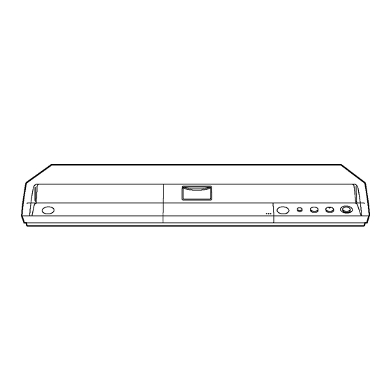
Page 15: Location Of Controls And Components
DMR-EH55EE / DMR-EH55GC / DMR-EH55GCS / DMR-EH55GN 6 Location of Controls and Components Followings are the Location of Controls and Components for DMR-EH55EC and DMR-EH56EG as a sample. For other model, refer to each Operation Instructions. - Page 16 DMR-EH55EE / DMR-EH55GC / DMR-EH55GCS / DMR-EH55GN...
-
Page 17: Operation Instructions
DMR-EH55EE / DMR-EH55GC / DMR-EH55GCS / DMR-EH55GN 7 Operation Instructions 7.1. Taking out the Disc from DVD-Drive Unit when the Disc cannot be ejected by OPEN/CLOSE button 7.1.1. Forcible Disc Eject 7.1.1.1. When the power can be turned off. 1. Turn off the power and press [STOP] [CH UP] keys on the front panel simultaneously for 5 seconds. -
Page 18: Service Mode
DMR-EH55EE / DMR-EH55GC / DMR-EH55GCS / DMR-EH55GN 8 Service Mode 8.1. Self-Diagnosis and Special Mode Setting 8.1.1. Self-Diagnosis Functions Self-Diagnosis Function provides information for errors to service personnel by “Self-Diagnosis Display” when any error has occurred. U**, H** and F** are stored in memory and held. - Page 19 DMR-EH55EE / DMR-EH55GC / DMR-EH55GCS / DMR-EH55GN Error Code Diagnosis contents Description Monitor Display Automatic FL display HARD Drive error The drive detected a hard error. “DVD drive error.” Display for 5 seconds. SELF Restoration operation Since the power cord fell out during a power...
- Page 20 DMR-EH55EE / DMR-EH55GC / DMR-EH55GCS / DMR-EH55GN Item FL display Key operation Mode name Description Front Key Forced disc eject Removing a disc that cannot be ejected. display before execution When the power is off, press The tray will open and unit will shift to P-off leaves.
- Page 21 DMR-EH55EE / DMR-EH55GC / DMR-EH55GCS / DMR-EH55GN Item FL display Key operation Mode name Description Front Key Demonstration Ejection of the disc is prohibited. *When lock the tray. When the power is on, press lock/unlock The lock setting is effective until unlocking the...
- Page 22 DMR-EH55EE / DMR-EH55GC / DMR-EH55GCS / DMR-EH55GN Item FL display Key operation Mode name Description (Remote controller key) White Picture Output White picture is output as component Output *Initial mode is “Interlace”. Press [1] [1] in service mode. from AV Decoder.
- Page 23 DMR-EH55EE / DMR-EH55GC / DMR-EH55GCS / DMR-EH55GN Item FL display Key operation Mode name Description (Remote controller key) HDD READ inspection Perform a complete read inspection of the When the HDD is OK Press [3] [1] in service mode. HDD.
- Page 24 DMR-EH55EE / DMR-EH55GC / DMR-EH55GCS / DMR-EH55GN Item FL display Key operation Mode name Description (Remote controller key) RAM Drive Last Error RAM Drive error code display. 1. Error Number is displayed for 5 Press [4] [2] in service mode.
- Page 25 DMR-EH55EE / DMR-EH55GC / DMR-EH55GCS / DMR-EH55GN Item FL display Key operation Mode name Description (Remote controller key) Front connection Press all front keys and check the connection Press [5] [4] in service mode. inspection between Main P.C.B. and Front key Switches.
- Page 26 DMR-EH55EE / DMR-EH55GC / DMR-EH55GCS / DMR-EH55GN Item FL display Key operation Mode name Description (Remote controller key) AV4(V)/AV1(RGB) Set input to AV4 (V) and set output to AV1 Press [8] [0] in service mode. Setting (RGB) for I/O checking...
-
Page 27: Service Fixture & Tools
DMR-EH55EE / DMR-EH55GC / DMR-EH55GCS / DMR-EH55GN 9 Service Fixture & Tools Part Number Description Compatibility RFKZ0260 Extension Cable (MainP.C.B. - RAM/Digital P.C.B. Module/ 88 Pin) Same as EH50 Series RFKZ0216 Extension Cable (MainP.C.B. - Power P.C.B./ 23 Pin) Same as E55 Series RFKZ0366 Extension FFC (HDD - RAM/Digital P.C.B. -
Page 28: Disassembly And Assembly Instructions
DMR-EH55EE / DMR-EH55GC / DMR-EH55GCS / DMR-EH55GN 10 Disassembly and Assembly Instructions 10.1. Disassembly Flow Chart The following chart is the procedure for disassembling the casing and inside parts for internal inspection when carrying out the servicing. To assemble the unit, reverse the steps shown in the chart below. -
Page 29: Top Case
DMR-EH55EE / DMR-EH55GC / DMR-EH55GCS / DMR-EH55GN 10.3. Top Case 10.5. SD Card P.C.B. 1. Remove 2 screws (A) and 3 screws (B). 1. Remove 1 FFC and 2 screws (A) to remove SD Card P.C.B.. 2. Slide Top Case rearward and open the both ends at rear side of the Top Case a little and lift the Top Case in the direction of the arrows. - Page 30 DMR-EH55EE / DMR-EH55GC / DMR-EH55GCS / DMR-EH55GN 1. Remove 1 FFC and 6 Screws (A). Note: 2. Lift up Digital P.C.B. slightly so to disconnect Connectors to RAM/Digital P.C.B. Module as service part has no heat sink remove Digital P.C.B.
-
Page 31: Dv Jack
DMR-EH55EE / DMR-EH55GC / DMR-EH55GCS / DMR-EH55GN 10.7. DV Jack P.C.B. 10.8. HDD 1. Remove 1 Screw (A) to remove DV Jack P.C.B. -
Page 32: Rear Panel
DMR-EH55EE / DMR-EH55GC / DMR-EH55GCS / DMR-EH55GN 1. Remove ATAPI Connector and HDD Power Connector. 2. Remove 4 Screws (A) to remove HDD Angle with HDD. 10.9. Rear Panel 1. Disconnect Fan Connector. 3. Put HDD with HDD Angle up and down inversely so as not to give a shock to HDD. -
Page 33: Power P.c.b
DMR-EH55EE / DMR-EH55GC / DMR-EH55GCS / DMR-EH55GN 10.10. Power P.C.B. 2. Remove 7 Screws (A) and 1 Screw (B). 1. Remove 1 Screw (A). 3. Unlock 2 Locking Tabs (A) to remove Rear Panel. 2. Remove 3 Screws (B) and disconnect Connector (A) to remove Power P.C.B.. -
Page 34: Main P.c.b. And Front (L)
DMR-EH55EE / DMR-EH55GC / DMR-EH55GCS / DMR-EH55GN 10.11. Main P.C.B. and Front (L) 10.12. Tuner P.C.B. P.C.B. 1. Pull out the Tuner P.C.B. in the direction of the arrow. 1. Remove 1 Screw (A). 2. Remove 4 Screws (A) and 1 Screw (B). -
Page 35: Measurements And Adjustments
DMR-EH55EE / DMR-EH55GC / DMR-EH55GCS / DMR-EH55GN 11 Measurements and Adjustments 11.1. Service Positions Note: For description of the disassembling procedure, see the section 10. 11.1.1. Checking and Repairing of Power P.C.B. - Page 36 DMR-EH55EE / DMR-EH55GC / DMR-EH55GCS / DMR-EH55GN 11.1.2. Checking and Repairing of RAM / Digital P.C.B. Module...
- Page 37 DMR-EH55EE / DMR-EH55GC / DMR-EH55GCS / DMR-EH55GN 11.1.3. Checking and Repairing of Main P.C.B.
- Page 38 DMR-EH55EE / DMR-EH55GC / DMR-EH55GCS / DMR-EH55GN 11.1.4. Checking and Repairing of HDD...
-
Page 39: Caution For Replacing Parts
DMR-EH55EE / DMR-EH55GC / DMR-EH55GCS / DMR-EH55GN 11.2. Caution for Replacing Parts 11.2.1. Items that should be done after replacing parts... - Page 40 DMR-EH55EE / DMR-EH55GC / DMR-EH55GCS / DMR-EH55GN Note3: Please prepare latest firmware updating disc. * Main Firm is being recorded in HDD, but new HDD has no data. Writing Procedure of Main Firm: <<Caution>> (1) Writing of Main Firm needs 3, 4 minutes.
-
Page 41: Standard Inspection Specifications After Making Repairs
Perform auto recording and playback for one minute using the RAM No abnormality should be seen in the picture, sound or operation. disc. *Panasonic DVD-RAM disc should be used when recording and playback. Model with the HDD: Perform auto recording and playback for one No abnormality should be seen in the picture, sound or operation. - Page 42 DMR-EH55EE / DMR-EH55GC / DMR-EH55GCS / DMR-EH55GN...
-
Page 43: Block Diagram
DMR-EH55EE / DMR-EH55GC / DMR-EH55GCS / DMR-EH55GN 12 Block Diagram 12.1. Power Supply Block Diagram POWER P.C.B. MAIN P.C.B. Q1700 T1150 (REG.X SW+3.8V) POWER SWITCHING TRANSFORMER VA1110,L1120 D1140,C1143 D1270 X SW+3.8V P1102 P1501 X SW+3.8V 16,17,19 AC INLET P1101 F1101... - Page 44 DMR-EH55EE / DMR-EH55GC / DMR-EH55GCS / DMR-EH55GN MAIN P.C.B. DIGITAL P.C.B. ANA+3.3V P7402 P59001 IC50001/IC53001/IC53003/IC57001(+3.3V) D+3.8V P7402 P59001 X SW+3.8V 60,62 IC59504 IC59506 ANA+5V P7402 P59001 IC50001/IC53003/IC53202/ (REG.D+3.3V) (REG.D+3.3V) IC4901- IC1506 IC53203(+5V) (REG.DR+5V) IC50001/IC55004/I IC50001/IC50002/ IP50002 VOUT VOUT C55006/IC57001(+3.3V) IC50004(+3.3V)
-
Page 45: Analog Video Block Diagram
DMR-EH55EE / DMR-EH55GC / DMR-EH55GCS / DMR-EH55GN 12.2. Analog Video Block Diagram :REC SIGNAL :PB SIGNAL IC3001 (VIDEO PROCESSOR) MAIN P.C.B. JK3903 (SW1) (SW2) COMP 6MHz P59001 P7402 C OUT DM 6MHz BIAS 12MHz (SW3) P59001 P7402 Y OUT DM... -
Page 46: Analog Audio Block Diagram
DMR-EH55EE / DMR-EH55GC / DMR-EH55GCS / DMR-EH55GN 12.3. Analog Audio Block Diagram :REC SIGNAL :PB SIGNAL MAIN P.C.B. JK3001 REAR JACK D4005 Q4006 MIX L OUT2 MUTE LINE OUT FROM XTMUTE TIMER Q4007 IC7501- QR4002-QR4004 SECTION MUTE MIX R OUT2... -
Page 47: Analog Timer Block Diagram
DMR-EH55EE / DMR-EH55GC / DMR-EH55GCS / DMR-EH55GN 12.4. Analog Timer Block Diagram IC7501 T7501 IR7501 (TIMER) DISPLAY HEATER POWER SWITCHING MAIN P.C.B. TRANSFORMER REMOTE CONTROL RECEIVER CTL. D7506 IP7501 P SAVE HEATER+ +38V UNREG.+38V PP7401 PS7801 (IC PROTECTOR) POWER SAVE... - Page 48 DMR-EH55EE / DMR-EH55GC / DMR-EH55GCS / DMR-EH55GN...
-
Page 49: Schematic Diagram
DMR-EH55EE / DMR-EH55GC / DMR-EH55GCS / DMR-EH55GN 13 Schematic Diagram 13.1. Interconnection Schematic Diagram JW7001 JW7501 PS57001 P37001 KEY3_POWER KEY3_POWER TPA+ TPA+ TPA- TPA- TPB+ TPB+ TPB- TPB- FRONT(L) P.C.B. P7402 P59001 DIGITAL P.C.B. DGND DGND DGND DGND DV JACK P.C.B. -
Page 50: Power Supply Schematic Diagram
DMR-EH55EE / DMR-EH55GC / DMR-EH55GCS / DMR-EH55GN 13.2. Power Supply Schematic Diagram LB1122 C1125 VWJ0795=5 ECKWNA102MEV ZA1103 ZA1104 D1140 EYF52BCY EYF52BCY B0EDKT000009 #K3GE1ZA00010 #K3GE1ZA00010 (S1WBA80-7062) L1120 G0B233D00001 K1122 C1121 VWJ0795=10 F1101 ECQU2A223MLC T1150 K5D202BK0005 ETS28BF1W6AD 250V T2AL P1101 D1270 K2AA2H000007... -
Page 51: Main Net (1/4) Section (Main P.c.b. (1/4)) Schematic
DMR-EH55EE / DMR-EH55GC / DMR-EH55GCS / DMR-EH55GN 13.3. Main Net (1/4) Section (Main P.C.B. (1/4)) Schematic Diagram (M) LOCATION MAP TUREG5V X_SW5R2V IC1510 C0CBCDG00006 (PG050DNA1ZPH) X_SW_3R3V RESET_5R2V M:Main Net Section:(Page: AV:A/V I/O Section:(Page: X_SW3R3 DE:Nicam Decoder Section:(Page: T:Timer Section:(Page: NOTE:DO NOT USE THE PART NUMBER SHOWN ON THIS DRAWING FOR ORDERRING. -
Page 52: Main Net (2/4) Section (Main P.c.b. (1/4)) Schematic
DMR-EH55EE / DMR-EH55GC / DMR-EH55GCS / DMR-EH55GN 13.4. Main Net (2/4) Section (Main P.C.B. (1/4)) Schematic Diagram (M) LOCATION MAP ZJ7402 K9ZZ00001279 ZJ7404 K9ZZ00001279 TO PS7801 TUNER PACK P.C.B. PP7401 K1KA18AA0288 BOOSTER5V TL7402 RFC_AUDIO[EB] RFC_AMUTE[EB] PS5V CPSVOUT[EB] QR7401 PS5V UNR521300L... -
Page 53: Main Net (3/4) Section (Main P.c.b. (1/4)) Schematic
DMR-EH55EE / DMR-EH55GC / DMR-EH55GCS / DMR-EH55GN 13.5. Main Net (3/4) Section (Main P.C.B. (1/4)) Schematic Diagram (M) MAIN NET SECTION (1/4) ANA5V P_OFF_L DR_P_ON_H HDD_PFAIL IC1506 DR12V Q1509 C0DAEYH00002 B1DHED000008 (UPA1717G-E1-A) DR5V TO P59001 ZJ7401 SOURSE VIN VOUT DIGITAL P.C.B. -
Page 54: Main Net (4/4) Section (Main P.c.b. (1/4)) Schematic Diagram (M)
DMR-EH55EE / DMR-EH55GC / DMR-EH55GCS / DMR-EH55GN 13.6. Main Net (4/4) Section (Main P.C.B. (1/4)) Schematic Diagram (M) MAIN NET SECTION (2/4) R7405 Q7401 ERDS2TJ471T 2SD1819AWL R7404 D7403 MA2C165001VT R7407 C7407 (MA165TA5VT) L7402 G0A220GA0026 R7406 R7408 470K LB7407 J0JKB0000012 QR7403... - Page 55 DMR-EH55EE / DMR-EH55GC / DMR-EH55GCS / DMR-EH55GN IC1510 IC1505 IC1521 IC7402 TU +5V SWITCHING REGULATOR XSW +3.3V SWITCHING REGULATOR ANA +3.3V SWITCHING REGULATOR BOOSTER +5V SWITCHING REGULATOR IC-DETAIL BLOCK DIAGRAM IC-DETAIL BLOCK DIAGRAM IC-DETAIL BLOCK DIAGRAM IC-DETAIL BLOCK DIAGRAM CONT...
-
Page 56: A/V I/O (1/4) Section (Main P.c.b. (2/4)) Schematic Diagram (Av)
DMR-EH55EE / DMR-EH55GC / DMR-EH55GCS / DMR-EH55GN 13.7. A/V I/O (1/4) Section (Main P.C.B. (2/4)) Schematic Diagram (AV) LOCATION MAP C4033 R4046 R4055 C4063 16V22 D0HB682ZA002 D0HB123ZA002 16V22 R4076 R4090 G_MIXLOUT_A R4077 M:Main Net Section:(Page: C4060 33P[22] D4005 R4002 AV:A/V I/O Section:(Page:... -
Page 57: A/V I/O (2/4) Section (Main P.c.b. (2/4)) Schematic
DMR-EH55EE / DMR-EH55GC / DMR-EH55GCS / DMR-EH55GN 13.8. A/V I/O (2/4) Section (Main P.C.B. (2/4)) Schematic Diagram (AV) LOCATION MAP M:Main Net Section:(Page: AV:A/V I/O Section:(Page: DE:Nicam Decoder Section:(Page: T:Timer Section:(Page: AV2-8PIN C3957 470P R3930 AV3_S_IN_L C3958 470P ZJ7501 JK3002... -
Page 58: A/V I/O (3/4) Section (Main P.c.b. (2/4)) Schematic
DMR-EH55EE / DMR-EH55GC / DMR-EH55GCS / DMR-EH55GN 13.9. A/V I/O (3/4) Section (Main P.C.B. (2/4)) Schematic Diagram (AV) A/V I/O SECTION (1/4) R4003 G_AADC_L_A R4005 G_AADC_R_A G_CIN_DM_A G_V_YIN_DM_A G_SLICER_A G_CSYNC_A G_IIC_CLK_A G_IIC_DATA_A SYNC_DET G_COUT_DM_A G_YOUT_DM_A G_BPBOUT_D_A G_RPROUT_D_A LB3001 PS_5V J0JGC0000020... -
Page 59: A/V I/O (4/4) Section (Main P.c.b. (2/4)) Schematic
DMR-EH55EE / DMR-EH55GC / DMR-EH55GCS / DMR-EH55GN 13.10. A/V I/O (4/4) Section (Main P.C.B. (2/4)) Schematic Diagram (AV) F G H N O P Q R S Z AA AB AC AD AE AG AH AI AJ AK AL AM... - Page 60 DMR-EH55EE / DMR-EH55GC / DMR-EH55GCS / DMR-EH55GN IC3001 IC4011 VIDEO/AUDIO PROCESSOR AU +5V SWITCHING REGULATOR IC-DETAIL BLOCK DIAGRAM IC-DETAIL BLOCK DIAGRAM VOUT (SW1) (SW2) COMP 6MHz 6MHz BIAS 12MHz (SW3) 6MHz CLAMP CLAMP/ BIAS (SW4) 6MHz COMP 12MHz CLAMP (SW6)
-
Page 61: Nicam Decoder Section (Main P.c.b. (3/4)) Schematic Diagram (De)
DMR-EH55EE / DMR-EH55GC / DMR-EH55GCS / DMR-EH55GN 13.11. Nicam Decoder Section (Main P.C.B. (3/4)) Schematic Diagram (DE) IC7301 RESET IC-DETAIL BLOCK DIAGRAM L7304 R7326 2.2u G_SIFIN_A R7322 G_TU_A_IN_A TU_REG5V K7308 ERJ3GEY0R00V Vref LB7304 L7303 LB7303 J0JHC0000032 G0C1R0JA0019 J0JCC0000080 K7303 IC7302... -
Page 62: Timer (1/4) Section (Main P.c.b. (4/4)) Schematic
DMR-EH55EE / DMR-EH55GC / DMR-EH55GCS / DMR-EH55GN 13.12. Timer (1/4) Section (Main P.C.B. (4/4)) Schematic Diagram (T) LOCATION MAP DP7501 A2BD00000145 TL7513 M:Main Net Section:(Page: AV:A/V I/O Section:(Page: DE:Nicam Decoder Section:(Page: T:Timer Section:(Page: FL10 FL23 FL09 [31]FL11 [20]FL22 FL24 FL08... -
Page 63: Timer (2/4) Section (Main P.c.b. (4/4)) Schematic
DMR-EH55EE / DMR-EH55GC / DMR-EH55GCS / DMR-EH55GN 13.13. Timer (2/4) Section (Main P.C.B. (4/4)) Schematic Diagram (T) LOCATION MAP M:Main Net Section:(Page: D7510 D7504 MA2C165001VT MAZ4220NLF AV:A/V I/O Section:(Page: L7501 G0C390JA0055 IP7501 DE:Nicam Decoder Section:(Page: ELESN390JA K5H7512A0010 T:Timer Section:(Page: R7615... -
Page 64: Timer (3/4) Section (Main P.c.b. (4/4)) Schematic
DMR-EH55EE / DMR-EH55GC / DMR-EH55GCS / DMR-EH55GN 13.14. Timer (3/4) Section (Main P.C.B. (4/4)) Schematic Diagram (T) TIMER SECTION (1/4) 97 96 92 91 87 86 84 83 CL7501 C7522 100P TL7515 R7516 22(EC) R7527 G_CSYNC_A VSYNC TL7509 R7528 FL_TXD... -
Page 65: Timer (4/4) Section (Main P.c.b. (4/4)) Schematic Diagram (T)
DMR-EH55EE / DMR-EH55GC / DMR-EH55GCS / DMR-EH55GN 13.15. Timer (4/4) Section (Main P.C.B. (4/4)) Schematic Diagram (T) M N O P Q TIMER SECTION (2/4) QR7507 UNR521000L RESET_5R2V IOPWR_SAVE_H R7586 D7502 R7583 R7584 B0ACCK000005 4700 (1SS355) TO JW7001 FRONT(L) P.C.B. -
Page 66: Tuner Pack Schematic Diagram
DMR-EH55EE / DMR-EH55GC / DMR-EH55GCS / DMR-EH55GN 13.16. Tuner Pack Schematic Diagram TO PP7401 MAIN P.C.B. C7828 K7808 C7809 (MAIN NET(2/4) SECTION) TU7801 0.01 ERJ3GEY0R00V 0.01 ENGF7502GF PS7801 LB7802 K1KB18B00012 J0JHC0000032 BOOSTER+B BOOSTER_5V RFC_AUDIO AUDIO IN RFC_A_MUTE MSDA PS_5V CPS_V_OUT... -
Page 67: Sd Card Schematic Diagram
DMR-EH55EE / DMR-EH55GC / DMR-EH55GCS / DMR-EH55GN 13.17. SD Card Schematic Diagram TO P53501 DIGITAL P.C.B. (BE(1/4) SECTION) P6802 SD CARD K1MY20AA0021 P6801 K1NA09E00075 SDAT1 DAT1 SCDA4A0200 SDAT0 DAT0 R6802 G_SCLK_B CKE9 DAT2 SCMD CKE1 C6801 RX6801 DAT3 0.01 SDAT3... -
Page 68: Front (L) Schematic Diagram
DMR-EH55EE / DMR-EH55GC / DMR-EH55GCS / DMR-EH55GN 13.18. Front (L) Schematic Diagram POWER TO JW7501 S7002 MAIN P.C.B. EVQ11A04M (TIMER(4/4) SECTION) JW7001 [VWJ02F0060VV] KEY3_POWER NOTE:DO NOT USE THE PART NUMBER SHOWN ON THIS DRAWING FOR ORDERRING. DMR-EH55EE/GC/GCS/GN THE CORRECT PART NUMBER IS SHOWN IN THE PARTS LIST,AND MAY BE SLIGHTLYDIFFERNT OR AMENDED SINCE THIS DRAWING WAS PREPARED. -
Page 69: Printed Circuit Board
DMR-EH55EE / DMR-EH55GC / DMR-EH55GCS / DMR-EH55GN 14 Printed Circuit Board 14.1. Power P.C.B. 203$&)24*454 !"#$%&'#$()*+&,-+# !""#$ !%& '(""$) (%& *"$++ *"-+- !%" ."$"+ /*""#+ (%& !""## !%& '(""$, *"$+" *"0++ ."&+" !%& *%& /*"$++ !""#& '(""$& *"$-+ <$/+/#0& ."&+$ (%&... -
Page 70: Main
DMR-EH55EE / DMR-EH55GC / DMR-EH55GCS / DMR-EH55GN 14.2. Main P.C.B. 14.2.1. Main P.C.B. (1/4 Section) (EE) Location Map (REAR) (FRONT) DMR-EH55EE/GC/GCS/GN Main P.C.B. ( RFKB79119JT:EH55EE, RFKB79119KT: EH55GC/GCS/GN) (1/4 Section) - Page 71 DMR-EH55EE / DMR-EH55GC / DMR-EH55GCS / DMR-EH55GN 14.2.2. Main P.C.B. (2/4 Section) Location Map (REAR) (FRONT) DMR-EH55EE/GC/GCS/GN Main P.C.B. ( RFKB79119JT:EH55EE, RFKB79119KT: EH55GC/GCS/GN) (2/4 Section)
- Page 72 DMR-EH55EE / DMR-EH55GC / DMR-EH55GCS / DMR-EH55GN 14.2.3. Main P.C.B. (3/4 Section) Main P.C.B. Location Map (REAR) (FRONT) DMR-EH55EE/GC/GCS/GN Main P.C.B. ( RFKB79119JT:EH55EE, RFKB79119KT: EH55GC/GCS/GN) (3/4 Section)
- Page 73 DMR-EH55EE / DMR-EH55GC / DMR-EH55GCS / DMR-EH55GN 14.2.4. Main P.C.B. (4/4 Section) Location Map (REAR) (FRONT) DMR-EH55EE/GC/GCS/GN Main P.C.B. ( RFKB79119JT:EH55EE, RFKB79119KT: EH55GC/GCS/GN) (4/4 Section)
- Page 74 DMR-EH55EE / DMR-EH55GC / DMR-EH55GCS / DMR-EH55GN 14.2.5. Main P.C.B. Address Information Main P.C.B. Integrated Circuit CL7508 LB3003 C1522 C3916 C7332 C7579 R3992 R7507 R7618 IC1505 TL3001 LB3005 C1523 C3917 C7333 C7584 R3993 R7508 R7619 IC1506 TL7401 LB3006 C1524 C3918...
-
Page 75: Tuner P.c.b. And Dv Jack P.c.b
DMR-EH55EE / DMR-EH55GC / DMR-EH55GCS / DMR-EH55GN 14.3. Tuner P.C.B. and DV Jack P.C.B. DV Jack P.C.B. Tuner P.C.B. DMR-EH55EE/GC/GCS/GN DMR-EH55EE/GC/GCS/GN Tuner P.C.B. DV Jack P.C.B. (VEP07A91D) (VEP73135A) -
Page 76: Sd Card P.c.b. And Front (L) P.c.b
DMR-EH55EE / DMR-EH55GC / DMR-EH55GCS / DMR-EH55GN 14.4. SD Card P.C.B. and Front (L) P.C.B. Front (L) P.C.B. SD Card P.C.B. DMR-EH55EE/GC/GCS/GN DMR-EH55EE/GC/GCS/GN SD Card P.C.B. Front (L) P.C.B. (VEP73136A) (VEP70161A) -
Page 77: Appendix For Schematic Diagram
DMR-EH55EE / DMR-EH55GC / DMR-EH55GCS / DMR-EH55GN 15 Appendix for Schematic Diagram 15.1. Voltage and Waveform Chart Note) Circuit voltage and waveform described herein shall be regarded as reference information when probing defect point, because it may differ from an actual measuring value due to difference of Measuring instrument and its measuring condition and product itself. - Page 78 DMR-EH55EE / DMR-EH55GC / DMR-EH55GCS / DMR-EH55GN IC4009 IC4011 Ref No. MODE 11.6 PLAY 11.6 STOP 11.6 IC4012 IC4901 Ref No. MODE 11.6 PLAY 11.6 STOP 11.6 Ref No. IC7301 MODE PLAY STOP Ref No. IC7301 MODE PLAY STOP IC7301 Ref No.
- Page 79 DMR-EH55EE / DMR-EH55GC / DMR-EH55GCS / DMR-EH55GN Q1501 Q1509 Ref No. MODE 12.4 12.4 12.4 12.3 12.3 12.3 12.3 PLAY 12.4 12.4 12.4 12.3 12.3 12.3 12.3 STOP 12.4 12.4 12.4 12.3 12.3 12.3 12.3 Ref No. Q4006 Q4007 Q4008...
- Page 80 DMR-EH55EE / DMR-EH55GC / DMR-EH55GCS / DMR-EH55GN 15.1.5. Waveform Chart T1150-12 STOP T1150-4,5 STOP IC1150-1 STOP T1150-8 STOP 10Vp-p (2m sec.div) 30Vp-p (5 sec.div) 10.0Vp-p (5 sec.div) 30Vp-p (5 sec.div) IC1150-9 STOP P7402-29,31 REC/PLAY P7402-51 REC/PLAY P7402-55 REC/PLAY 580Vp-p (5 sec.div) 0.8Vp-p (1m sec.div)
- Page 81 DMR-EH55EE / DMR-EH55GC / DMR-EH55GCS / DMR-EH55GN 15.1.6. Abbreviations INITIAL/LOGO ABBREVIATIONS INITIAL/LOGO ABBREVIATIONS A0~UP ADDRESS IECOUT IEC958 FORMAT DATA OUTPUT ACLK AUDIO CLOCK IPFRAG INTERPOLATION FLAG AD0~UP ADDRESS BUS IREF I (CURRENT) REFERENCE ADATA AUDIO PES PACKET DATA ISEL INTERFACE MODE SELECT...
- Page 82 DMR-EH55EE / DMR-EH55GC / DMR-EH55GCS / DMR-EH55GN INITIAL/LOGO ABBREVIATIONS TRACKING ERROR TIBAL BALANCE CONTROL BALANCE OUTPUT 1 BALANCE INPUT BALANCE INPUT BALANCE OUTPUT 2 TPSN OP AMP INPUT TPSO OP AMP OUTPUT TPSP OP AMP INVERTED INPUT TRCRS TRACK CROSS SIGNAL...
-
Page 83: Parts And Exploded Views
DMR-EH55EE / DMR-EH55GC / DMR-EH55GCS / DMR-EH55GN 16 Parts and Exploded Views 16.1. Exploded Views 16.1.1. Casing Parts & Mechanism Section... - Page 84 DMR-EH55EE / DMR-EH55GC / DMR-EH55GCS / DMR-EH55GN 16.1.2. Packing & Accessories Section...
-
Page 85: Replacement Parts List
DMR-EH55EE / DMR-EH55GC / DMR-EH55GCS / DMR-EH55GN 16.2. Replacement Parts List Ref. Part No. Part Name & Remarks Description C1706 ECJ1VB1H103K 50V 0.01U Notes: C1707 F2A0J6810007 6.3V 680P *Important safety notice: C1800 F2A1E4700048 25V 47U Components identified mark have special... - Page 86 DMR-EH55EE / DMR-EH55GC / DMR-EH55GCS / DMR-EH55GN Ref. Part No. Part Name & Remarks Ref. Part No. Part Name & Remarks Description Description R1800 ERJ6GEYJ471V 1/8W 470 C3003 ECJ1VB1C104K 16V 0.1U R1801 ERJ6GEYJ104V 1/8W 100K C3004 ECJ1VB1C104K 16V 0.1U R1802 ERJ6GEYJ472V 1/8W 4.7K...
- Page 87 DMR-EH55EE / DMR-EH55GC / DMR-EH55GCS / DMR-EH55GN Ref. Part No. Part Name & Remarks Ref. Part No. Part Name & Remarks Description Description C4034 F2A1C220B173 16V 22P C7523 ECJ1VB1H103K 50V 0.01U C4055 ECJ1VF1C104Z 16V 0.1U C7524 ECJ1VB1C104K 16V 0.1U C4056...
- Page 88 DMR-EH55EE / DMR-EH55GC / DMR-EH55GCS / DMR-EH55GN Ref. Part No. Part Name & Remarks Ref. Part No. Part Name & Remarks Description Description IC7504 C0HBB0000044 LB7416 J0JCC0000164 COIL IC7505 C0EBJ0000336 LB7417 J0JCC0000103 COIL IC7507 C0ABBA000073 LB7418 J0JCC0000103 COIL LB7419 J0JCC0000103...
- Page 89 DMR-EH55EE / DMR-EH55GC / DMR-EH55GCS / DMR-EH55GN Ref. Part No. Part Name & Remarks Ref. Part No. Part Name & Remarks Description Description R3059 ERJ3GEYJ750V 1/10W 75 R7324 ERJ3GEYJ221V 1/10W 220 R3060 ERJ3GEYJ750V 1/10W 75 R7325 ERJ3GEYJ221V 1/10W 220 R3061...
- Page 90 DMR-EH55EE / DMR-EH55GC / DMR-EH55GCS / DMR-EH55GN Ref. Part No. Part Name & Remarks Ref. Part No. Part Name & Remarks Description Description R7587 ERJ3GEYJ224V 1/10W 220K W529 ERJ6GEY0R00V 1/8W 0 R7588 ERJ3GEYJ104V 1/10W 100K W530 ERJ6GEY0R00V 1/8W 0 R7589...
- Page 91 DMR-EH55EE / DMR-EH55GC / DMR-EH55GCS / DMR-EH55GN Ref. Part No. Part Name & Remarks Ref. Part No. Part Name & Remarks Description Description W521 ERJ8GEY0R00V 1/4W 0 RHD30113 SCREW W523 ERJ6GEY0R00V 1/8W 0 RFKV0069HDK HDD 160GB W524 ERJ3GEY0R00V 1/10W 0...
Need help?
Do you have a question about the DMR-EH55EE and is the answer not in the manual?
Questions and answers