
Subscribe to Our Youtube Channel
Related Manuals for Panasonic SHOWSTOPPER PV-SS2710


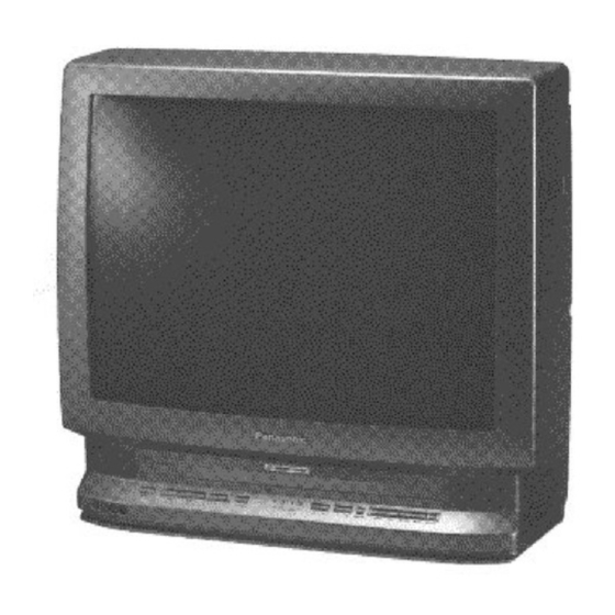
Summary of Contents for Panasonic SHOWSTOPPER PV-SS2710
- Page 1 ORDER NO. MKE0101751C1 TV/Hard Disk Recorder Combination PV-SS2710 SPECIFICATIONS 2001 Matsushita-Kotobuki Electronics Industries LTD. All rights www.manualscenter.com...
- Page 2 reserved. Unauthorized copying and distribution is a violation of law. 1. SAFETY PRECAUTIONS 1.1. GENERAL GUIDELINES 1. IMPORTANT SAFETY NOTICE There are special components used in this equipment which are important for safety. These parts are marked by in the Schematic Diagrams, Circuit Board Layout, Exploded Views and Replacement Parts List.
- Page 3 resistance than specified, as follows : B+ Line Minimum Resistance 130 V (Hot chassis ground) 27 V (Cold chassis ground) 17 V (Cold chassis ground) 6. When the TV set is not used for a long period of time, unplug the power cord from the AC outlet.
- Page 4 2. Connect a 1.5 k , 10 W resistor, in parallel with a 0.15 F capacitor, between each exposed metallic part on the set and a good earth ground , as shown in Figure 1. 3. Use an AC voltmeter, with 1 k /V or more sensitivity, to measure the potential across the resistor.
- Page 5 3. Measure the High Voltage. The meter reading should indicate 30.0 kV± 2.0 kV. If the meter indication is out of tolerance, immediate service and correction is required to prevent the possibility of premature component failure. 4. To prevent an X-Radiation possibly, it is essential to use the specified picture tube.
- Page 6 3. PREVENTION OF ELECTROSTATIC DISCHARGE (ESD) TO ELECTROSTATICALLY SENSITIVE (ES) DEVICES Some semiconductor (solid state) devices can be damaged easily by static electricity. Such components commonly are called Electrostatically Sensitive (ES) Devices. Examples of typical ES devices are integrated circuits and some field-effect transistors are semiconductor "chip" components.
- Page 7 Be sure no power is applied to the chassis or circuit, and observe all other safety precautions. 8. Minimize bodily motions when handling unpackaged replacement ES devices. (Otherwise harmless motion such as the brushing together of your clothes fabric or the lifting of your foot from a carpeted floor can generate static electricity (ESD) sufficient to damage an ES device).
- Page 8 Check the signal at the following wires and TPs. / Refer to “Check points and Waveforms for service position (1).” Fig. 1-1-2 Fig. 1-1-3 www.manualscenter.com...
- Page 9 5.1.1.1.2. Service Position (2) 1. Remove the Rear Cover and the TV/Video/Power/HDR Unit. Then, remove the C.B.A.s from the Bottom Frame. 2. Remove the PCB Holder Piece from the Bottom Frame as shown. Fig. 1-2-1...
- Page 10 3. Place the Main C.B.A. and TV Main C.B.A. on the Table. Then, connect the Connector P7004 and P551. 4. In order to stabilize C.B.A.s, attach the PCB Holder Piece to both C.B.A.s as shown. Fig. 1-2-2 5. Place it along with Guide ribs on the Bottom Frame. Service Position (2) Fig.
- Page 11 Note: 1. It is only possible to use the LINE3 input terminal (on the A/V Jack C.B.A.) in this position to connect with the Input source. 2. After servicing, attach the PCB Holder Piece in the place of the Bottom Frame.
- Page 12 absorbent mat. Also, be careful when transporting HDD. B. Be careful not to subject HDD to any shock when tightening screws for HDD replacement. (Tighten screws manually, not with an electric driver.) 2. MOISTURE A. Moisture may also be a damaging factor. HDD is semi-closed style. Sudden changes in ambient temperature may cause moisture to form.
- Page 13 (the replacement HDD carton). 5.1.3. HOW TO WATCH THE TV WITHOUT THE HDD AND HDR MAIN C.B.A. The unit works as a TV after removing the HDD and the HDR Main C.B.A. When both the HDD and the HDR Main C.B.A. are removed, be sure to disconnect all cables from the HDD (2 Cables) and the HDR Main C.B.A.
- Page 14 Note: 1. After replacing the HDD, press SELECT button on the unit in this mode. Only Total elapsed "HDD Active" time (in hours) will be cleared to 0. 2. FAN ACTIVE displayed on the TV monitor shows the total elapsed "Fan Locked"...
- Page 15 3. Press and hold STOP, VOL -, and EXIT buttons on the unit together over 5 seconds again or press the POWER button OFF to release EVR Adjustment Mode. The Default value will be written to Memory IC (IC6001). 4. Perform all EVR Adjustments. (Refer to "EVR (Electronic Variable Register) ADJUSTMENT WITH THE REMOTE CONTROL"...
- Page 16 Fig. 5-2...
- Page 17 5.1.10. HOT CIRCUIT Primary circuit exists on the TV Main C.B.A. and the Power Supply C.B.A. This circuit is identified as "HOT" on the C.B.A. and in the Service Manual. Use extreme care to prevent accidental shock when servicing. 5.1.11. VARIABLE VOLTAGE ISOLATION TRANSFORMER An Isolation Transformer should always be used during the servicing of HDR Combination whose chassis is not isolated from the AC power line.
- Page 18 Leadless capacitor must be preheated before installation. -(266 °F ~ 302 °F) (130 °C ~150 °C) for about two minutes. Note: A. Leadless components must not be reused after removal. B. Excessive mechanical stress and rubbing of the component electrode must be avoided. 2.
- Page 19 5.2. IC, TRANSISTOR AND CHIP PART INFORMATION 6. DISASSEMBLY/ASSEMBLY PROCEDURES 6.1. CABINET SECTION 6.1.1. Disassembly Flowchart Perform all disassembly procedures in the order described in the "Disassembly Flowchart" shown below. When reassembling, use the reverse procedure.
- Page 20 CAUTION: Disconnect AC plug before disassembly. Fig. D1 6.1.2. Disassembly Method www.manualscenter.com...
- Page 21 Fig. D2...
- Page 22 Fig. D3...
- Page 23 6.1.2.1. Notes in chart 1. Removal of TV/Video/Power/HDR Unit Fig. D4 www.manualscenter.com...
- Page 24 2. Removal of CRT Unit Place the Unit face down on a soft cloth before removing the CRT Unit. 3. Removal/Installation of Hard Disk Drive A. Use extreme care when removing or installing the Hard Disk Drive. (Refer to "HANDLING PRECAUTIONS FOR HDD"...
- Page 25 1. Dual-Trace Oscilloscope Voltage Range: 0.001 V to 50 V/Div. Frequency Range: DC to 50 MHz Probes: 10:1, 1:1 2. NTSC Video Pattern Generator 3. MTS/SAP Signal Generator (TV Multi-Channel Sound Modulator (U.S.A.)) 4. Plastic Tip Driver and Non-Metal Driver 5.
- Page 26 Adjustment : R4906, R4914 (Main C.B.A.) Specification : minimum level INPUT : Antenna Input Terminal MTS (ONLY L CH) 300 Hz±5 Hz, 3 kHz±5 Hz 14 % or 7 % Modulating Mode : STEREO audio (TV) Equipment : Oscilloscope, MTS/SAP Signal Generator 1.
- Page 27 7.1.4. SEPARATION ADJUSTMENT Note: Be sure to perform this adjustment after STEREO/SAP SEPARATION ADJUSTMENT are completed. Purpose: To separate the L and R Channels of Stereo Signal. Symptom of Misadjustment: The L and R Channels of Stereo Signal will not be separated properly resulting in no stereophonic effect.
- Page 28 3. Set to TV mode, and then set to STEREO audio. 4. Adjust R4902 (SEPARATION) on the Main C.B.A. so that the signal level is minimum. Fig. E3 7.1.5. EVR (Electronic Variable Register) ADJUSTMENT WITH THE REMOTE CONTROL This unit has electronic technology using I C Bus concept.
- Page 29 The adjustment overlay will appear to enter EVR adjustment mode. Fig. E4-1 7.1.7.1. How to adjust: www.manualscenter.com...
- Page 30 7.1.7.2. How to release from EVR Adjustment Mode: Press and hold STOP, VOL-, and EXIT buttons on the unit together over 5 seconds again or press the POWER button OFF. The adjusted value will be written to Memory IC (IC6001). 7.1.8.
- Page 31 Note: Before pressing DISPLAY key on the remote control for collapse scan, select the desired control function and move the shaded area to the value for adjustments you will proceed. Fig. E4-6 7.1.8.1. How to release from Service Mode: Press DISPLAY key again on the remote control. 7.1.9.
- Page 32 3. Select SUB BRIGHT in EVR adjustment mode. Then, after making a note of the original value, adjust to the (D0). 4. Select SUB CONTRAST in EVR adjustment mode and adjust so that the level A is 3.0 V[p-p]±0.1 V[p-p]. 5.
- Page 33 Video Input Jack, Monoscope Pattern Signal Mode : STOP Equipment : Oscilloscope, NTSC Video Pattern Generator 1. Supply a Monoscope Pattern Signal to the Video Input Jack. 2. Connect the Oscilloscope to TP50 on the CRT C.B.A. (Use TP47 for GND.) 3.
- Page 34 adjust the B CUT -OFF and G CUT -OFF. 10. Press DISPLAY key on the remote control again to return for full frame scan. 11. Select SUB BRIGHT in EVR adjustment mode and adjust so that the picture has adequate brightness. 12.
- Page 35 on the CRT C.B.A. 4. Select SUB TINT in EVR adjustment mode and adjust so that level A and B should be equal in amplitude. Fig. E7-1 5. Select SUB COLOR in EVR adjustment mode and adjust so that the level C is 1.50 V[p-p]±0.15 V[p-p].
- Page 36 V POSITION (EVR) Specification : Refer to descriptions below. Input : Video Input Jack, Monoscope Pattern Signal Mode : STOP Equipment : NTSC Video Pattern Generator 1. Supply a Monoscope Pattern Signal to the Video Input Jack. 2. Select H CENTER in EVR adjustment mode and adjust so that A is approximately equal to width B.
- Page 37 7.1.13. WHITE BALANCE ADJUSTMENT Purpose: To set the standard white level for each color temperature. Symptom of Misadjustment : White becomes bluish or reddish. Test Point : TP50 (CRT C.B.A) Adjustment : FOCUS CONTROL (Flyback Transformer), SCREEN CONTROL (Flyback Transformer), SUB BRIGHT (EVR), G DRIVE (EVR), B DRIVE (EVR),...
- Page 38 Input : Video Input Jack, Monoscope Pattern Signal, White Pattern Signal Mode : STOP Equipment : NTSC Video Pattern Generator, White Pattern Generator, Oscilloscope 1. Supply a Monoscope Pattern Signal to the Video Input Jack. 2. Connect the Oscilloscope to TP50 on the CRT C.B.A. (Use TP47 for GND.) 3.
- Page 39 9. In EVR adjustment mode, select the two colors not observed in step 8 from the following control functions (B CUT -OFF, G CUT -OFF, or R CUT -OFF) and adjust so that the horizontal line becomes white. For example, if the horizontal line appeared red in step 8, select and adjust the B CUT -OFF and G CUT -OFF.
- Page 40 Mode : STOP 1. Do not input any signal to the unit. 2. Set INPUT SELECT item to LINE in SET UP TV menu to display black screen. 3. Select SUB BRIGHT in EVR adjustment mode, and adjust so that the black screen starts to turn grey (lighting only).
- Page 41 8.2. MAIN / INFRARED / OPERATION SCHEMATIC DIAGRAMS 8.3. POWER SUPPLY SCHEMATIC DIAGRAMS 8.4. TV MAIN SCHEMATIC DIAGRAM 8.5. VERTICAL SCHEMATIC DIAGRAM 8.6. AUDIO/VIDEO JACK SCHEMATIC DIAGRAM 8.7. CRT SCHEMATIC DIAGRAM 8.8. INTERCONNECTION SCHEMATIC DIAGRAM 8.9. I/O CHART OF EACH CONNECTOR BETWEEN MAIN C.B.A./POWER SUPPLY C.B.A.
- Page 42 12.2. CHASSIS FRAME SECTION(2)
- Page 43 12.3. CHASSIS FRAME SECTION(3) www.manualscenter.com...
- Page 44 12.4. PACKING PARTS AND ACCESSORIES SECTION...
- Page 45 13. REPLACEMENT PARTS LISTS BEFORE REPLACING PARTS, READ THE FOLLOWING: 13.1. REPLACEMENT NOTES 13.1.1. General Notes 1. Use only original replacement parts: To maintain original function and reliability of repairedunits, use only...
- Page 46 original replacement parts which arelisted with their part numbers in the parts list. 2. IMPORTANT SAFETY NOTICE Components identified by the sign have special characteristics important for safety. When replacing any of these components, use only the specified parts. 3. SPECIAL NOTE All integrated circuits and many other semiconductor devices are electrostatically sensitive and therefore require the special handling techniques described underthe "ELECTROSTATICALLY SENSITIVE...
- Page 47 All coils are in H, M = 1,000 2. Abbreviation RTL: Retention Time Limited This indicates that the retention time is limited for this item. After the discontinuation of this item in production, it will no longer be available. Non Repairable Board Ass'y MGF CHIP: Metal Glaze Film Chip C CHIP:...
- Page 48 with remote control. 7. D1010 and D1011 replacement note: Although D1010 and D1011 have Ref. No. for diode,they are ICs. 13.2. MECHANICAL REPLACEMENT PARTS LIST Ref. No. Part No. Part Name & Description Remarks LXQVB01279 PICTURE TUBE UNIT 1 MKA LSYK0477 FRONT CABINET ASS'Y 1 MKA...
- Page 49 Ref. No. Part No. Part Name & Description Remarks VEKS5783 CONNECTOR CABLE W/PLUG,DC 1V 2 MKA VEKS5784 CONNECTOR CABLE W/PLUG,DC 1V 2 MKA VEKS5785 CONNECTOR CABLE W/PLUG,DC 1V 2 MKA VEKS5786 CONNECTOR CABLE W/PLUG,DC 5V 2 MKA LSYY0010 HDR UNIT 2 E.S.D.
- Page 50 13.3. ELECTRICAL REPLACEMENT PARTS LIST 13.3.1. PRINTED CIRCUIT BOARD ASSEMBLY Ref. No. Part No. Part Name & Description Remarks VEPS3089A MAIN C.B.A. E.S.D. RTL MKA VEPS0A97A INFRARED C.B.A. RTL MKA VEPS1019A POWER SUPPLY C.B.A. RTL MKA LRP61012A TV MAIN C.B.A. RTL MKA LRP63019C VERTICAL C.B.A.
- Page 51 Ref. No. Part No. Part Name & Description Remarks Q3001 2SC2412K1 CHIP OR 2SD601A CHIP Q3002 2SC2412K1 CHIP OR 2SD601A CHIP Q3003 2SA1037K146R CHIP OR 2SB709A CHIP Q3004 2SC2295(C) CHIP Q3005 2SA1037K146R CHIP OR 2SB709A CHIP Q3006 2SC2412K1 CHIP OR 2SD601A CHIP Q3007 2SA1037K146R CHIP...
- Page 52 Ref. No. Part No. Part Name & Description Remarks Q5303 2SC2412K1 CHIP OR 2SD601A CHIP Q5304 2SC2412K1 CHIP OR 2SD601A CHIP Q5501 2SA1037K146R CHIP OR 2SB709A CHIP Q5502 2SC2295(C) CHIP Q5503 2SA1037K146R CHIP OR 2SB709A CHIP Q5504 2SA1037K146R CHIP OR 2SB709A CHIP Q5505 DTC114YK...
- Page 53 Ref. No. Part No. Part Name & Description Remarks OR 1SS133T D6006 MA165 OR 1SS119 OR 1SS133T D6501 MA728 CHIP D6502 SLP313C81HAB LED GREEN D6503 SLP913C81HAB LED RED D6504 SLP313C81HAB LED GREEN D6505 SLP913C81HAB LED RED RESISTORS...
- Page 54 Ref. No. Part No. Part Name & Description Remarks R3001 ERJ6ENF1001V MGF CHIP 1/10W 1K R3002 ERJ6GEYJ102V MGF CHIP 1/10W 1K R3003 ERJ6ENF1001V MGF CHIP 1/10W 1K R3004 ERJ6GEYJ681V MGF CHIP 1/10W 680 R3006 ERJ6GEYJ331V MGF CHIP 1/10W 330 R3007 ERJ6ENF4700V MGF CHIP 1/10W 470 R3008...
- Page 55 Ref. No. Part No. Part Name & Description Remarks R3056 ERJ6GEY0R00V MGF CHIP 1/10W 0 R3057 ERJ6GEY0R00V MGF CHIP 1/10W 0 R3058 ERJ6GEY0R00V MGF CHIP 1/10W 0 R3059 ERJ6GEYJ102V MGF CHIP 1/10W 1K R3060 ERJ6GEYJ152V MGF CHIP 1/10W 1.5K R3061 ERJ6GEYJ104V MGF CHIP 1/10W 100K R4001 ERJ6GEYJ102V MGF CHIP 1/10W 1K...
- Page 57 Ref. No. Part No. Part Name & Description Remarks R4902 EVNCYAA03B14 VARIABLE 10K R4903 ERJ6GEYJ102V MGF CHIP 1/10W 1K R4904 ERJ6GEYJ122V MGF CHIP 1/10W 1.2K R4905 ERJ6GEYJ104V MGF CHIP 1/10W 100K R4906 EVNCYAA03B14 VARIABLE 10K R4907 ERJ6GEYG683V MGF CHIP 1/10W 68K R4908 ERJ6GEYJ105V MGF CHIP 1/10W 1M R4909...
- Page 58 Ref. No. Part No. Part Name & Description Remarks R5348 ERJ6GEYJ101V MGF CHIP 1/10W 100 R5350 ERJ6GEYJ272V MGF CHIP 1/10W 2.7K R5352 ERJ6GEYJ272V MGF CHIP 1/10W 2.7K R5353 ERJ6GEYJ222V MGF CHIP 1/10W 2.2K R5354 ERDS2TJ471 R5355 ERJ6GEYJ473V MGF CHIP 1/10W 47K R5356 ERJ6GEYJ151V MGF CHIP 1/10W 150 R5357...
- Page 60 Ref. No. Part No. Part Name & Description Remarks R6039 ERJ6GEYJ472V MGF CHIP 1/10W 4.7K R6040 ERJ6GEYJ103V MGF CHIP 1/10W 10K R6041 ERJ6GEYJ103V MGF CHIP 1/10W 10K R6042 ERJ6GEYJ563V MGF CHIP 1/10W 56K R6043 ERJ6GEYJ102V MGF CHIP 1/10W 1K R6044 ERJ6GEYJ102V MGF CHIP 1/10W 1K R6054 ERJ6GEYJ102V MGF CHIP 1/10W 1K...
- Page 62 Ref. No. Part No. Part Name & Description Remarks R6122 ERJ6GEYJ221V MGF CHIP 1/10W 220 R6123 ERJ6GEYJ223V MGF CHIP 1/10W 22K R6124 ERDS2TJ222 2.2K R6125 ERJ6GEYJ562V MGF CHIP 1/10W 5.6K R6126 ERJ6GEYJ153V MGF CHIP 1/10W 15K R6128 ERJ6GEYJ223V MGF CHIP 1/10W 22K R6133 ERJ6GEY0R00V MGF CHIP 1/10W 0 R6134...
- Page 63 Ref. No. Part No. Part Name & Description Remarks R6545 ERJ6GEYJ103V MGF CHIP 1/10W 10K R6546 ERJ6GEYJ103V MGF CHIP 1/10W 10K R6547 ERJ6GEYJ103V MGF CHIP 1/10W 10K R6548 ERJ6GEYJ103V MGF CHIP 1/10W 10K R6549 ERJ6GEYJ103V MGF CHIP 1/10W 10K R6550 ERJ6GEYJ103V MGF CHIP 1/10W 10K R6551 ERJ6GEYJ103V MGF CHIP 1/10W 10K...
- Page 64 Ref. No. Part No. Part Name & Description Remarks C4014 ECUV1H104ZFN C CHIP 50V 0.1 C4015 ECUV1H104ZFN C CHIP 50V 0.1 C4016 ECEA1CKA100 ELECTROLYTIC 16V 10 C4017 ECUV1H104ZFN C CHIP 50V 0.1 C4018 ECEA0JKA470 ELECTROLYTIC 6.3V 47 C4025 ECUV1H104ZFN C CHIP 50V 0.1 C4026 ECEA0JKA470 ELECTROLYTIC 6.3V 47...
- Page 66 Ref. No. Part No. Part Name & Description Remarks C4918 ECEA1CKA100 ELECTROLYTIC 16V 10 C4919 ECEA1CKA100 ELECTROLYTIC 16V 10 C4920 ECEA1CKA100 ELECTROLYTIC 16V 10 C5303 ECUV1H103ZFN C CHIP 50V 0.01 C5304 ECEA1CKN100 ELECTROLYTIC 16V 10 C5305 ECEA1CKN100 ELECTROLYTIC 16V 10 C5306 ECEA1CKA470 ELECTROLYTIC 16V 47...
- Page 67 Ref. No. Part No. Part Name & Description Remarks C6005 ECUV1H101JCN C CHIP 50V 100P C6008 ECUV1E104ZFN C CHIP 25V 0.1 C6010 ECUV1H103ZFN C CHIP 50V 0.01 C6012 ECUV1H020CCN C CHIP 50V 2P C6013 ECUV1H150GCN C CHIP 50V 15P C6014 ECUV1H180JCN C CHIP 50V 18P C6016 ECEA0JKA470...
- Page 68 Ref. No. Part No. Part Name & Description Remarks X5301 VSXS0208-A X5302 CSB503F38 X6001 VSXS0784 X6002 VSXS0238 X6501 EF0EC8384T4 PIN HEADERS Ref. No. Part No. Part Name & Description Remarks P3001 VJPS0276 CONNECTOR 6P P3002 VJPS0277 CONNECTOR 7P P3003 VJPS0771 CONNECTOR PLUG 13P P3004 VJPS0267...
- Page 69 13.3.3. INFRARED C.B.A. INTEGRATED CIRCUITS Ref. No. Part No. Part Name & Description Remarks IC6351 PNA4611M00YA INFRARED RECEIVER UNIT RESISTORS Ref. No. Part No. Part Name & Description Remarks R6351 ERDS2TJ560 CAPACITORS Ref. No. Part No. Part Name & Description Remarks C6351 VCYSHRE104ZF CERAMIC 25V 0.1...
- Page 70 Ref. No. Part No. Part Name & Description Remarks Q1001 2SK2996 Q1101 2SD601(R,S) CHIP Q1201 2SA1037K146R CHIP OR 2SB709A CHIP Q1202 2SC2412K1 CHIP OR 2SD601(R,S) CHIP Q1203 2SD2097TV2R CHIP OR 2SD235800A CHIP Q1204 2SD1119(R) CHIP Q1205 2SC2412K1 CHIP OR 2SD601(R,S) CHIP Q1206 2SD2097TV2R CHIP...
- Page 71 Ref. No. Part No. Part Name & Description Remarks D1001 ERZV10D241 SURGE ABSORBER 240V D1002 D3SBA60-4101 D1003 MA111 CHIP D1004 MA4300-L ZENER 30V D1005 MA165 D1006 MA4300-L ZENER 30V D1007 ERA18-04V3 D1008 MA8200-L ZENER CHIP 20V OR UDZTE-1720B ZENER CHIP 20V D1009 ERA18-04V3 D1010...
- Page 72 RESISTORS Ref. No. Part No. Part Name & Description Remarks R1002 LSRJA8J224V MGF CHIP 1/8W 220K R1003 LSRJA8J274V MGF CHIP 1/8W 270K R1004 LSRJA6J823V MGF CHIP 1/10W 82K R1005 LSRJA8J104V MGF CHIP 1/8W 100K R1006 LSRJA8J124V MGF CHIP 1/8W 120K R1007 LSRJA8J331V MGF CHIP 1/8W 330...
- Page 73 Ref. No. Part No. Part Name & Description Remarks R1214 ERJ6GEYJ104V MGF CHIP 1/10W 100K R1301 ERG1SJ101P METAL OXIDE 1W 100 R1302 ERG1SJ101P METAL OXIDE 1W 100 R1303 ERDS2T0 R1304 LSRJA6J102V MGF CHIP 1/10W 1K R1305 LSRJA6J102V MGF CHIP 1/10W 1K R1306 LSRJA6J102V MGF CHIP 1/10W 1K...
- Page 74 Ref. No. Part No. Part Name & Description Remarks R1541 ERG1SJ150E METAL OXIDE 1W 15 CAPACITORS Ref. No. Part No. Part Name & Description Remarks C1001 ECQU2A683MLC POLYESTER 250V 0.068 C1002 ECUV1H104KBN C CHIP 50V 0.1 C1003 ECA2DHG221E ELECTROYTIC 200V 220 C1004 ECUV1E222KBN C CHIP 25V 2200P...
- Page 75 Ref. No. Part No. Part Name & Description Remarks C1302 ECUV1H104ZFN C CHIP 50V 0.1 C1303 ECEA1EKA470B ELECTROLYTIC 25V 47 C1304 ECEA0JKA470 ELECTROLYTIC 6.3V 47 C1305 ECUV1H104ZFN C CHIP 50V 0.1 C1306 ECEA0JKA470 ELECTROLYTIC 6.3V 47 C1307 ECUV1H104ZFN C CHIP 50V 0.1 C1308 ECUV1H104ZFN C CHIP 50V 0.1...
- Page 76 FUSE & PROTECTOR Ref. No. Part No. Part Name & Description Remarks F1001 LSSF0046 FUSE 125V 1.6A PR1101 UNH000400A IC PROTECTOR OR ICP-N25T104 IC PROTECTOR PR1102 UNH000400A IC PROTECTOR OR ICP-N25T104 IC PROTECTOR PR1104 UNH000400A IC PROTECTOR OR ICP-N25T104 IC PROTECTOR PR1201 UNH000400A IC PROTECTOR...
- Page 77 Ref. No. Part No. Part Name & Description Remarks Q501 2SC2482KT Q551 2SD2539LBK Q571 2SC2785(TH) OR 2SC2785(TJ) OR 2SC945A(TQ) Q581 2SA1321TPE6 OR 2SA1767(Q) OR 2SB1221(Q) Q801 2SC2785(TH) OR 2SC2785(TJ) OR 2SC945A(TQ) DIODES Ref. No. Part No. Part Name & Description Remarks D503 ERB43-04V...
- Page 78 Ref. No. Part No. Part Name & Description Remarks R501 ERDS2TJ681 R502 ERDS2TJ332 3.3K R505 ERDS2TJ561 R511 ERG3FJ272H METAL OXIDE 3W 2.7K R513 ERG12SJ560P METAL OXIDE 1/2W 56 R516 LAR05222J09 W FLMPRF 5W 2.2K R552 ERDS2TJ103 R553 ERDS2TJ102 R554 ERDS2TJ822 8.2K R555 ERDS2TJ683...
- Page 79 Ref. No. Part No. Part Name & Description Remarks C501 ECQB1H473KM POLYESTER 50V 0.047 C510 ECKW2H681KB5 CERAMIC 500V 680P C513 ECA1HM100B ELECTROLYTIC 50V 10 C524 ECKC3D471KBP CERAMIC 2KV 470P C531 ECA1HM3R3B ELECTROLYTIC 50V 3.3 C552 ECA1EM471E ELECTROLYTIC 25V 470 C553 ECKW2H221KB5 CERAMIC 500V 220P C554...
- Page 80 PIN HEADERS Ref. No. Part No. Part Name & Description Remarks P551 VJSS0876 CONNECTOR RECEPTACLE 19P P552 VJSS0898 4P WIRE TRAP P801 VJPS0303 CONNECTOR 2P P7004 VJSS0875 CONNECTOR RECEPTACLE 13P FUSE & PROTECTOR Ref. No. Part No. Part Name & Description Remarks F801 LSSF012B040...
- Page 81 TRANSISTORS Ref. No. Part No. Part Name & Description Remarks Q431 2SA1175 OR 2SA1175(TH) OR 2SA733(TQ) Q432 2SC3311A(R) Q433 2SB1322A(R,S) Q434 2SC3311A(R) Q502 2SC2785(TH) OR 2SC2785(TJ) OR 2SC945A(TQ) Q541 2SA1175 OR 2SA1175(TH) OR 2SA733(TQ) Q542 2SC2785(TH) OR 2SC2785(TJ) OR 2SC945A(TQ) DIODES Ref.
- Page 82 Ref. No. Part No. Part Name & Description Remarks R401 ERDS2TJ561 R402 ERDS2TJ103 R405 ERG2SJ561H METAL OXIDE 2W 560 R406 ERDS2TJ334 330K R409 ERJ6GEYJ273V MGF CHIP 1/10W 27K R410 ERDS2TJ272 2.7K R411 ERDS2TJ104 100K R413 ERJ6GEYJ333V MGF CHIP 1/10W 33K R414 ERX1SJ1R2P METAL OXIDE 1W 1.2...
- Page 83 Ref. No. Part No. Part Name & Description Remarks C401 ECEA1HGE2R2 ELECTROLYTIC 50V 2.2 C402 ECA1CM471B ELECTROLITIC 16V 470 C408 ECA1HGE010KB ELECTROLYTIC 50V 1 C409 ECA1VM101B ELECTROLYTIC 35V 100 C413 ECQB1H104KF POLYESTER 50V 0.1 C414 ECA1CM222E C418 ECA1VM221B ELECTROLYTIC 35V 220 C458 ECQB1H103KM POLYESTER 50V 0.01 C541...
- Page 84 Ref. No. Part No. Part Name & Description Remarks D4591 RD9.1EW ZENER 9.1V D4592 MA165-TA5.VT D4593 MA165-TA5.VT D4789 MA165-TA5.VT D4790 MA165-TA5.VT D4797 MA165-TA5.VT D4798 MA165-TA5.VT RESISTORS Ref. No. Part No. Part Name & Description Remarks R4591 ERDS2TJ681 R4592 ERDS2TJ681 R4593 ERDS2TJ681 R4594 ERDS2TJ681...
- Page 85 Ref. No. Part No. Part Name & Description Remarks R351 ERG2ANJ153H METAL OXIDE 2W 15K R352 ERG2ANJ153H METAL OXIDE 2W 15K R353 ERG2ANJ153H METAL OXIDE 2W 15K R354 ERD25TJ272 2.7K R355 ERD25TJ272 2.7K R356 ERD25TJ272 2.7K R357 ERDS2TJ332 3.3K R358 ERDS2TJ332 3.3K R359...
- Page 86 NOTE: FOR SCHEMATIC DIAGRAM AND CIRCUIT BOARD LAYOUT NOTES, REFER TO BEGINNING OF SCHEMATIC SECTION. MAIN C.B.A. (VIDEO/AUDIO SECTION) MODE STOP MODE STOP MODE STOP MODE STOP MODE STOP MODE STOP MODE STOP MODE STOP MODE STOP MODE STOP MODE STOP PIN NO.
- Page 87 NOTE: FOR SCHEMATIC DIAGRAM AND CIRCUIT BOARD LAYOUT NOTES, REFER TO BEGINNING OF SCHEMATIC SECTION. MAIN C.B.A. (SYSTEM CONTROL/SERVO SECTION) MODE PLAY MODE PLAY MODE PLAY MODE PLAY MODE PLAY MODE PLAY MODE PLAY MODE PLAY MODE PLAY PIN NO. PIN NO.
- Page 88 NOTE: FOR SCHEMATIC DIAGRAM AND CIRCUIT BOARD LAYOUT NOTES, REFER TO BEGINNING OF SCHEMATIC SECTION. INFRARED VERTICAL AUDIO/VIDEO JACK POWER SUPPLY C.B.A TV MAIN C.B.A. C.B.A. CRT C.B.A. C.B.A. C.B.A. MODE STOP MODE STOP MODE STOP MODE STOP MODE STOP MODE STOP MODE...
- Page 89 1. Important safety notice 3. Parts enclosed in dashed lines marked "Z" are not used Components identified by the sign have special in any models included in this service manual. characteristics important for safety. When replacing any Example: of these components. Use only the specified parts. C3010 0.01 2.
- Page 90 INTERCONNECTION SCHEMATIC DIAGRAM IMPORTANT SAFETY NOTICE: COMPONENTS IDENTIFIED BY THE SIGN HAVE SPECIAL CHARACTERISTICS IMPORTANT FOR SAFETY. HDR MAIN C.B.A. HARD DISK DRIVE FAN MOTOR WHEN REPLACING ANY OF THESE COMPONENTS, P9074 P9023 (9 Pins) (40 Pins) USE ONLY THE SPECIFIED PARTS. P9031 (12 Pins) NOTE:...
- Page 91 CRT SCHEMATIC DIAGRAM NOTE: NOTE: IMPORTANT SAFETY NOTICE: FOR SCHEMATIC DIAGRAM AND CIRCUIT BOARD LAYOUT NOTES, PARTS ENCLOSED IN DASHED LINES MARKED "Z" ARE NOT USED. COMPONENTS IDENTIFIED BY THE SIGN HAVE REFER TO BEGINNING OF SCHEMATIC SECTION. SPECIAL CHARACTERISTICS IMPORTANT FOR SAFETY. WHEN REPLACING ANY OF THESE COMPONENTS, USE ONLY THE SPECIFIED PARTS.
- Page 92 AUDIO/VIDEO JACK SCHEMATIC DIAGRAM NOTE: FOR SCHEMATIC DIAGRAM AND CIRCUIT BOARD LAYOUT NOTES, REFER TO BEGINNING OF SCHEMATIC SECTION. D4799 J4791 D4790 NOTE: REC VIDEO SIGNAL REC AUDIO SIGNAL PB AUDIO SIGNAL MA165-TA5.VT PARTS ENCLOSED IN DASHED LINES MARKED "Z" ARE NOT USED. TO TV MAIN D4797 C.B.A.
- Page 93 VERTICAL SCHEMATIC DIAGRAM NOTE: NOTE: FOR SCHEMATIC DIAGRAM AND CIRCUIT BOARD LAYOUT NOTES, PARTS ENCLOSED IN DASHED LINES MARKED "Z" ARE NOT USED. REFER TO BEGINNING OF SCHEMATIC SECTION. IMPORTANT SAFETY NOTICE: COMPONENTS IDENTIFIED BY THE SIGN HAVE SPECIAL CHARACTERISTICS IMPORTANT FOR SAFETY. WHEN REPLACING ANY OF THESE COMPONENTS, Q542 USE ONLY THE SPECIFIED PARTS.
- Page 94 TV MAIN SCHEMATIC DIAGRAM NOTE: NOTE: FOR SCHEMATIC DIAGRAM AND CIRCUIT BOARD LAYOUT NOTES, PARTS ENCLOSED IN DASHED LINES MARKED "Z" ARE NOT USED. REFER TO BEGINNING OF SCHEMATIC SECTION. TO VERTICAL C.B.A. P451/P452 REC VIDEO SIGNAL REC AUDIO SIGNAL DISCHARGE TV POWER ON(H) BLANKING PULSE...
- Page 95 POWER SUPPLY I SCHEMATIC DIAGRAM NOTE:THE VOLTAGE FOR PARTS IN HOT CIRCUIT CAUTION: FOR CONTINUED PROTECTION AGAINST FIRE HAZARD, IMPORTANT SAFETY NOTICE: NOTE: IS MEASURED USING POWER HEAT SINK REPLACE ONLY WITH THE SAME TYPE 1.6A 125V FUSE. COMPONENTS IDENTIFIED BY THE SIGN HAVE FOR SCHEMATIC DIAGRAM AND CIRCUIT BOARD LAYOUT NOTES, AS A COMMON TERMINAL.
- Page 96 POWER SUPPLY II SCHEMATIC DIAGRAM NOTE: FOR SCHEMATIC DIAGRAM AND CIRCUIT BOARD LAYOUT NOTES, REFER TO BEGINNING OF SCHEMATIC SECTION. PB VIDEO SIGNAL REC AUDIO SIGNAL REC VIDEO SIGNAL PB AUDIO SIGNAL UNSW+12V 1 NOTE: R1541 15/1W PARTS ENCLOSED IN DASHED LINES MARKED "Z" ARE NOT USED. TO HDR MAIN J1501 JK1501...
- Page 97 MAIN I / INFRARED SCHEMATIC DIAGRAM NOTE: FOR SCHEMATIC DIAGRAM AND CIRCUIT BOARD LAYOUT NOTES, REFER TO BEGINNING OF SCHEMATIC SECTION. Q6005 SWITCHING MUTE-ON R6142 VOLUME CONTROL TO MAIN IV TO MAIN IV UNSW+5V(D) SERIAL DATA 1 C6042 10/16V SERIAL DATA 0 TO MAIN II TO MAIN II UNSW+5V(D)
- Page 98 MAIN II / OPERATION SCHEMATIC DIAGRAM NOTE: NOTE: REFER TO "I/O CHART OF EACH CONNECTOR BETWEEN MAIN C.B.A./ FOR SCHEMATIC DIAGRAM AND CIRCUIT BOARD LAYOUT NOTES, POWER SUPPLY C.B.A. AND HDR MAIN C.B.A." REFER TO BEGINNING OF SCHEMATIC SECTION. P6501 R6506 HDR SERIAL DATA 0 R6507...
- Page 99 MAIN III SCHEMATIC DIAGRAM NOTE: PARTS ENCLOSED IN DASHED LINES MARKED "Z" ARE NOT USED. TO MAIN I TO MAIN IV TO MAIN I REC VIDEO SIGNAL NOTE: PB VIDEO SIGNAL FOR SCHEMATIC DIAGRAM AND CIRCUIT BOARD LAYOUT NOTES, REFER TO BEGINNING OF SCHEMATIC SECTION. IMPORTANT SAFETY NOTICE: R5301 COMPONENTS IDENTIFIED BY THE SIGN...
- Page 100 IC5301 LUMINANCE/CHROMINANCE PROCESS IC-DETAIL BLOCK DIAGRAM, AN5367FB REC VIDEO SIGNAL PB VIDEO SIGNAL S P O T K I L L E R B L A C K L E V E L D E T E C T O R D E T E C T O R A C C A C C...
- Page 101 *2,*3,*4 NOTE: MAIN IV SCHEMATIC DIAGRAM NOTE: NOTE: REFER TO "I/O CHART OF EACH CONNECTOR BETWEEN MAIN C.B.A./ FOR SCHEMATIC DIAGRAM AND CIRCUIT BOARD LAYOUT NOTES, PARTS ENCLOSED IN DASHED LINES MARKED "Z" ARE NOT USED. POWER SUPPLY C.B.A. AND HDR MAIN C.B.A." REFER TO BEGINNING OF SCHEMATIC SECTION.
- Page 102 (1) MAIN C.B.A. (2) POWER SUPPLY C.B.A. P3002 (TO HDR MAIN C.B.A. P9032) P1301 (TO HDR MAIN C.B.A. P9019) Pin No. I/O Signal Name Description Pin No. I/O Signal Name Description HDR AUDIO(L) HDR L-channel audio signal HDR+12V Power supply terminal(unsw+12V) Grounding terminal HDR+12V Power supply terminal(unsw+12V)
- Page 103 VERTICAL C.B.A. LRP63019C CRT C.B.A. LRP63005E NOTE: NOTE: CIRCUIT BOARD LAYOUT INCLUDES COMPONENTS WHICH ARE NOT USED. CIRCUIT BOARD LAYOUT INCLUDES COMPONENTS WHICH ARE NOT USED. PLEASE REFER TO THE SCHEMATIC DIAGRAM AND PARTS LIST FOR PROPER PARTS CONTENT. PLEASE REFER TO THE SCHEMATIC DIAGRAM AND PARTS LIST FOR PROPER PARTS CONTENT. IMPORTANT SAFETY NOTICE: CAUTION: WHEN SERVICING THIS C.B.A., AVOID TOUCHING HIGH VOLTAGE COMPONENTS.
- Page 104 TV MAIN C.B.A. LRP61012A www.manualscenter.com R560 C812 T502 C510 R511 P7004 T501 P551 COLD C813 J554 U801 R516 IC801 R807 J555 Q501 U551 Q551 TP501 TP893 R584 TP502 R583 R582 R581 C563 R805 C571 E C B Q581 R806 R802 L802 C531 C556...
- Page 105 www.manualscenter.com POWER SUPPLY C.B.A. VEPS1019A P1201 JK1503 R1532 P1504 COLD D1509 D1513 R1530 D1508 D1516 R1533 AUDIO D1502 D1510 R1314 IN/OUT R1131 D1506 D1517 L1102 R1516 R1519 R1315 P1001 R1517 D1204 R1528 R1121 D1505 D1512 R1529 R1208 D1507 D1518 R1102 F1001 1.6A 125V R1514 R1539...
- Page 106 NOTE: NOTE: MAIN C.B.A. VEPS3089A IMPORTANT SAFETY NOTICE: CIRCUIT BOARD LAYOUT INCLUDES COMPONENTS WHICH ARE NOT USED. FOR SCHEMATIC DIAGRAM AND CIRCUIT BOARD LAYOUT NOTES, COMPONENTS IDENTIFIED BY THE SIGN HAVE www.manualscenter.com PLEASE REFER TO THE SCHEMATIC DIAGRAM AND PARTS LIST FOR PROPER PARTS CONTENT. REFER TO BEGINNING OF SCHEMATIC SECTION.
- Page 107 MAIN C.B.A. TV MAIN C.B.A. U7001 UHF/VHF TUNER/TV DEMODULATOR UNIT IC6002 (TV MICROCONTROLLER) P6002 P6002 SERIAL DATA 0 P6002 P6002 SERIAL CLOCK P6002 P6002 RESET(L) TUNER CS(L) TUNER CS(H) IC6003 (OSD/CCV MICROCONTROLLER) X6001 OSC 2 14.3MHz OSD CS(L) OSD CS(L) OSC 1 SERIAL DATA 0 SERIAL DATA 1...
- Page 108 4.6 Vp-p 4.6 Vp-p 4.8 Vp-p 20 µs 20 µs 20 µs VIDEO SIGNAL MAIN C.B.A. CRT C.B.A. 2 Vp-p 0.34 Vp-p X5301 130 Vp-p 130 Vp-p 3.58MHz OSC TP47 IC5301 (LUMINANCE/CHROMINANCE PROCESS) 0.1 V 20 µs 0.5 V 20 µs 3.58MHz 50 V 20 µs...
- Page 109 REC AUDIO SIGNAL PB AUDIO SIGNAL MAIN C.B.A. POWER SUPPLY C.B.A. IC4004 (OP AMP) IC4201(OP AMP) Q4202 P3003 P1504 AUDIO OUT(L) P3002 BUFFER HDR AUDIO (L) Q4201 P3003 P1504 AUDIO OUT(R) P3002 BUFFER HDR AUDIO (R) P3006 LINE AUDIO 1(L) P3006 LINE AUDIO 2(L) TO/FROM...
- Page 110 REC VIDEO SIGNAL PB VIDEO SIGNAL TV MAIN C.B.A. MAIN C.B.A. IC3301 (Y/C SEPA) NOT USED Q3302 Q3301 BUFFER BUFFER Q3304 J5503 BUFFER Q3303 Q3305 SEPARATION BUFFER BUFFER NOT USED Q7001 Q5300 BUFFER (FROM IC5301(31)) UHF/VHF TUNER/TV 358MHz DEMODULATOR UNIT J5502 IC5502 (INPUT SELECT) J7001...
- Page 111 TV MAIN C.B.A. POWER SUPPLY C.B.A. V1 17.5 Vp-p T1001 (SWITCHING TRANSFORMER) 5 µs +5.1V F801 F1001 L801 L1001 D1002 4A/125V 1.6A/125V L1101, TP1205 P801 P1001 TP804 D1101 C1104,1109 Q1203 PR1101 LINE LINE FULL-WAVE SW+5.1V(A) RECTIFIER SMOOTHING CORD P801 FILTER FILTER RECTIFIER TP803...
- Page 112 VIDEO & AUDIO SIGNAL PATH (HDR MODE) VIDEO & AUDIO SIGNAL PATH (BYPASS MODE) VIDEO SIGNAL PATH (HDR MODE) VIDEO SIGNAL PATH (BYPASS MODE) AUDIO SIGNAL PATH (HDR MODE) AUDIO SIGNAL PATH (BYPASS MODE) POWER SUPPLY C.B.A. MAIN C.B.A. CRT C.B.A. HDR MAIN C.B.A.
- Page 113 Note: Before doing troubleshooting: 1. Confirm that a signal is being output from the input sources (Cable Box, DSS Receiver, or Antenna) and that the input sources are properly and securely connected to the unit. 2. If using the IR Blaster, confirm that the IR Blaster is properly affixed to the external devices (Cable Box, DSS Receiver, etc.) for CH control. 3.
- Page 114 Symptoms Possible Solution No Video on the TV monitor and/ Both Video and Audio NG Change to BYPASS mode by pressing BYPASS button and confirm that the picture is Main C.B.A. is defective. Repair Main C.B.A. or No Audio from the Speaker. being displayed on the TV monitor and the audio can be heard from the speaker.
- Page 115 Symptoms Possible Solution Can not control the CH of Cable Confirm that the Serial Cable is securely connected to the external devices(Cable Box or DSS Receiver) If not, connect it securely. Box or DSS Receiver by using the Serial cable. Still NG Confirm that the Setup has been carried out properly.
Need help?
Do you have a question about the SHOWSTOPPER PV-SS2710 and is the answer not in the manual?
Questions and answers