Table of Contents
Advertisement
Quick Links
[1]
Precaution for using lead-free solder ..... . ....... 1-1
[2]
Safety precaution for service manual..... . ....... 1-2
[3]
Voltage selection ........................................... 1-2
[4]
Ac power supply cord............................. . ....... 1-2
[5]
Specifications ......................................... . ....... 1-3
[6]
Names of parts ....................................... . ....... 1-4
[1]
Mechanism section ................................ . ....... 2-1
[2]
Deck section........................................... . ....... 2-1
[3]
Tuner section.......................................... . ....... 2-2
[4]
Test Mode............................................... . ....... 2-3
[5]
CD Section .................................................... 2-5
[1]
Caution on disassembly ......................... . ....... 3-1
[1]
Main Block diagrams.............................. . ....... 4-1
[2]
CD Servo Block diagrams ............................. 4-3
!
Parts marked with "
" are important for maintaining the safety of the set. Be sure to replace these parts with specified ones
for maintaining the safety and performance of the set.
SERVICE MANUAL
MODEL
In the interests of user-safety the set should be restored to its
original condition and only parts identical to those specified be
used.
CONTENTS
CHAPTER 5. CIRCUIT DESCRIPTION
[1]
Waveforms of CD Servo Circuit.....................5-1
[2]
Voltage...........................................................5-2
[1]
Notes on schematic diagram .........................6-1
[2]
Types of transistor and LED ..........................6-1
[3]
Schematic diagram ........................................6-2
[4]
Wiring side of PWB......................................6-10
[1]
Troubleshooting .............................................7-1
[1]
Function table of IC........................................8-1
[2]
LCD Display.................................................8-10
This document has been published to be used
for after sales service only.
The contents are subject to change without notice.
- 1
GX-CD5100W
No. S4613GXCD5100
PORTABLE CD STEREO
COMPONENT SYSTEM
GX-CD5100W
Advertisement
Table of Contents

Related Manuals for Sharp GX-CD5100W


Summary of Contents for Sharp GX-CD5100W
-
Page 1: Table Of Contents
GX-CD5100W SERVICE MANUAL No. S4613GXCD5100 PORTABLE CD STEREO COMPONENT SYSTEM GX-CD5100W MODEL In the interests of user-safety the set should be restored to its original condition and only parts identical to those specified be used. CONTENTS PRECAUTIONS FOR USING LEAD FREE SOLDER CHAPTER 5. -
Page 2: Precautions For Using Lead Free Solder
GX-CD5100W CHAPTER 1. GENERAL DESCRIPTION Audio XL-MP150 Service Manual XLMP150 Market [1] PRECAUTIONS FOR USING LEAD-FREE SOLDER 1. Employing lead-free solder "MAIN,DISPLAY,POWER KEY,POWER SUPPLY,HEADPHONE,TAPE 1 KNOB,TAPE 2 KNOB,FLASH, CD SERVO of this model employs lead-free solder. The LF symbol indicates lead-free solder, and is attached on the PWB and service manuals.The alphabetical character following LF shows the type of lead-free solder. -
Page 3: Safety Precaution For Service Manual
Copying or broadcasting such material without permission of the relevant in licenses or owners of the copyright is prohibited by law. SHARP is not in a position to authorise the copying or broadcasting of copyright materials and nothing in this OPERATION MANUAL should be implied as giving that authority. -
Page 4: Specifications
FOR A COMPLETE DESCRIPTION OF THE OPERATION OF THIS UNIT, PLEASE REFER TO THE OPERATION MANUAL. As part of our policy of continuous improvement, SHARP reserves the right to make design and specifcation changes for product improvement without prior notice. The performance specification figures indicated are nominal values of production units .There maybe some deviations from these... -
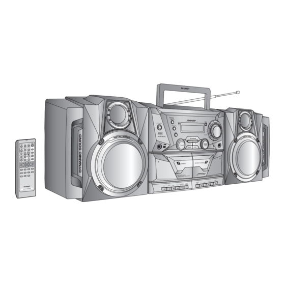
Page 5: Names Of Parts
GX-CD5100W [6] NAMES OF PARTS Controls and indicators 1. Disc Compartment Front panel 1. Tape 1 Cassette Compartment 2. Built in Microphone 3. Headphone Socket 4. Tuning Down Button 5. Tuning Up Button 6. Line In Button PUSH OPEN/CLOSE 7. On/Stand by Button 8. - Page 6 GX-CD5100W Controls and indicators (continued) Rear Panel 1. AM Loop Aerial Socket 2. Beat Cancel 3. CD/LINE Input Socket 4. Speaker Terminals 5. AC Power Lead 6. Voltage Selector 7. Battery Compartment 8. DC Power Terminal Speaker system 1. Tweeter 2.
- Page 7 GX-CD5100W Display 1. Disc Pause Indicator 2. Disc Play Indicator 3. Disc Repeat Play Indicator 4. Tape Continuous Playback Indicator 5. Extra Bass Indicator 6. Memory Indicator 7. CD Indicator 8. MP3 Indicator 9. High Speed Dubbing Indicator 10. Random Indicator 12 13 11.
-
Page 8: Chapter 2. Adjustments
GX-CD5100W CD-ES700/CD-ES77 CD-ES700/CD-ES77 Service Manual CD-ES700/CD-ES77 Market CHAPTER 2. ADJUSTMENTS [1] MECHANISM SECTION • Driving Force Check Torque Meter Specified Value Play: TW-2412 Tape 1: Over 72 g Tape 2: Over 72 g • Torque Check Torque Meter Specified Value... -
Page 9: Tuner Section
GX-CD5100W [3]TUNER SECTION fL: Low-range frequency • Setting the Test Mode fH: High-renge frequency Keeping the T1(STOP) button and T2(STOP) button, pressed • AM IF/RF TUNER button. Then, the frequency is initially set in the memory Signal generator: 400 Hz, 30%, AM modulated as shown in Table. -
Page 10: Test Mode
GX-CD5100W [4] TEST MODE Setting the test mode During stand-by mode, press ON/STAND-BY button while pressing down the TAPE 2 STOP button and TAPE 1 STOP button then, press the CD STOP button to enter the test mode. T E S T IL isn’t done... - Page 11 GX-CD5100W <<MEMORY>> key input. Laser ON. <<MEMORY>> key input. Tracking OFF play at that specific point. <<MEMORY>> key input. Tracking ON play from that specific point. <<MEMORY>> key input. Adjustment result automatically will display as below for each 2 sec : a) "FOF_XXXX"...
-
Page 12: Cd Section
GX-CD5100W [5] CD SECTION Adjustment Since this CD system incorporates the following automatic adjustment functions, readjustment is not needed when replacing the pickup. Therefore, different PWBs and pickups can be combined freely. Each time a disc is changed, these adjustments are performed automatically. -
Page 13: Chapter 3. Mechanism Blocks
GX-CD5100W CHAPTER 3. MECHANISM BLOCKS CD-ES700/CD-ES77 CD-ES700/CD-ES77 Service Manual CD-ES700/CD-ES77 Market CHAPTER 3. [1] Caution on disassembly Caution on Disassembly Follow the below-mentioned notes when disassembling the unit and reassembling it, to keep it safe and ensure excellent performance: 1. Take cassette tape and compact disc out of the unit. - Page 14 GX-CD5100W Figure 4 Figure 7 Figure 5 Figure 8 Figure 6 3 – 2...
-
Page 15: Chapter 4. Diagrams
GX-CD5100W CHAPTER 4. DIAGRAMS CHAPTER 5. [1] Main Block diagrams Figure 4-1: BLOCK DIAGRAM (1/4) 4 – 1... - Page 16 GX-CD5100W Figure 4-2: BLOCK DIAGRAM (2/4) 4 – 2...
-
Page 17: Cd Servo Block Diagrams
GX-CD5100W [2] CD Servo Block Diagrams Figure 4-3: BLOCK DIAGRAM (3/4) 4 – 3... - Page 18 GX-CD5100W Figure 4-4: BLOCK DIAGRAM (4/4) 4 – 4...
- Page 19 GX-CD5100W CHAPTER 5. CIRCUIT DISCRIPTION CHAPTER 5. [1] WAVEFORMS OF CD CIRCUIT SPDO RFOUT LRSY PDOUT 0 DATACK PDOUT 1 DATA RFOUT 5 – 1...
-
Page 20: Voltage
GX-CD5100W [2] Voltage Q703 Q103 Q102 Q308 Q303 Pin No. Voltage (V) Pin No. Voltage (V) Pin No. Voltage (V) Pin No. Voltage (V) Pin No. Voltage (V) 4.84 0.00 0.70 8.12 0.00 0.10 0.00 0.00 8.78 0.00 0.00 0.00 0.00... - Page 21 GX-CD5100W IC401 IC101 IC701 IC303 (LC75341) (AN7345K) (MICOM- IXA098AW) (LC72131) Pin No. Voltage (V) Pin No. Voltage (V) Pin No. Voltage (V) Pin No. Voltage (V) Pin No. Voltage (V) 0.00 0.00 4.91 0.02 2.07 0.00 0.00 4.81 4.81 0.00 0.00...
- Page 22 GX-CD5100W (LC78690 ) (LA6548NH ) Pin No. Voltage (V) Pin No. Voltage (V) Pin No. Voltage (V) 1.60 5.86 3.28 1.77 5.56 0.00 1.73 1.64 3.25 1.54 1.64 1.54 2.60 1.64 2.60 Pin No. Voltage (V) 1.64 0.00 5.62 1.64 0.00...
-
Page 23: Chapter 6. Circuit Schematics And Parts Layout
GX-CD5100W CHAPTER 6. CIRCUIT SCHEMATICS AND PARTS LAYOUT CIRCUIT SCHEMATICS AND PARTS LAYOUT CHAPTER 6. Notes on schematic diagram Resistor: • The indicated voltage in each section is the one • measured by Digital Multimeter between such a To differentiate the units of resistors, such symbol section and the chassis with no signal given. -
Page 24: Schematic Diagram
GX-CD5100W [3] SCHEMATIC DIAGRAM Figure 6-1: MAIN SCHEMATIC DIAGRAM (1/8) 6 – 2... - Page 25 GX-CD5100W Figure 6-2: MAIN SCHEMATIC DIAGRAM (2/8) 6 – 3...
- Page 26 GX-CD5100W Figure 6-3: DISPLAY SCHEMATIC DIAGRAM (3/8) 6 – 4...
- Page 27 GX-CD5100W Figure 6-4: DISPLAY SCHEMATIC DIAGRAM (4/8) 6 – 5...
- Page 28 GX-CD5100W FM SIGNAL MW / SW1 / SW2 SIGNAL Figure 6-5: DISPLAY SCHEMATIC DIAGRAM (5/8) 6 – 6...
- Page 29 GX-CD5100W Figure 6-6: DISPLAY SCHEMATIC DIAGRAM (6/8) 6 – 7...
- Page 30 GX-CD5100W PICK UP UNIT Figure 6-7: CD MP3 SCHEMATIC DIAGRAM (7/8) 6 – 8...
- Page 31 GX-CD5100W NOTES ON SCHEMATIC DIAGRAM can be found on page 6-1 The numbers are waveform numbers shown in page 5-1 Figure 6-8: CD MP3 SCHEMATIC DIAGRAM (8/8) 6 – 9...
-
Page 32: Wiring Side Of Pwb
GX-CD5100W [4] Wiring side of PWB ROD ANTENNA (239) SO401 CD/LINE INPUT R-ch L-ch ANTENNA SPRING SW101 AM LOOP (227) BEAT ANTENNA CANCEL B C E E C B E C B E C B E C B E C B... - Page 33 GX-CD5100W Lead-free solder indication L-ch Lead-free solder is used in the MAIN, HEADPHONE PWB. Refer to "Precautions for handling lead-free solder" for instructions and precautions. SCREW TO TAPE MECHANISM CHASIS HEADPHONE PWB-A5 JK801 HEADPHONE E C B 2 3 4 5 6 7 Figure 6-10: WIRING SIDE OF PWB (2/15) 6 –...
- Page 34 GX-CD5100W Figure 6-11: WIRING SIDE OF PWB (3/15) 6 – 12...
- Page 35 GX-CD5100W Figure 6-12: WIRING SIDE OF PWB (4/15) 6 – 13...
- Page 36 GX-CD5100W Figure 6-13: WIRING SIDE OF PWB (5/15) 6 – 14...
- Page 37 GX-CD5100W -MEMO- 6 – 15...
- Page 38 GX-CD5100W Figure 6-14: WIRING SIDE OF PWB (6/15) 6 – 16...
- Page 39 GX-CD5100W Figure 6-15: WIRING SIDE OF PWB (7/15) 6 – 17...
- Page 40 GX-CD5100W Figure 6-16: WIRING SIDE OF PWB (8/15) 6 – 18...
- Page 41 GX-CD5100W Figure 6-17: WIRING SIDE OF PWB (9/15) 6 – 19...
- Page 42 GX-CD5100W Figure 6-18: WIRING SIDE OF PWB (10/15) 6 – 20...
- Page 43 GX-CD5100W Figure 6-19: WIRING SIDE OF PWB (11/15) 6 – 21...
- Page 44 GX-CD5100W 1 2 3 4 5 6 7 Figure 6-20: WIRING SIDE OF PWB (12/15) 6 – 22...
- Page 45 GX-CD5100W CD MOTOR PWB Figure 6-21: WIRING SIDE OF PWB (13/15) 6 – 23...
- Page 46 GX-CD5100W CD SERVO PWB-C (BOTTOM VIEW) Figure 6-22: WIRING SIDE OF PWB (14/15) 6 – 24...
- Page 47 GX-CD5100W The number are waveform number shown in page 5-1 Figure 6-23: WIRING SIDE OF PWB (15/15) 6 – 25...
-
Page 48: Chapter 7. Flowchart
GX-CD5100W CHAPTER 7. FLOWCHART [1] Troubleshooting 1. When the CD does not function The CD section may not operate when the objective lens of the optical pickup is dirty. Clean the objective lens, and check the playback operation. When this section does not operate even after the above step is taken, check the follow- ing items. - Page 49 GX-CD5100W (1) Focus-RF system check. Although a CD is inserted and the cover is closed, "NO DISC" is displayed. Push Open/Close Button without inserting a disc, and try starting the playback operation. Figure 1 1. Does the pickup move to the PICKUP-IN Switch (NSW1) Sled motor (NM2).
- Page 50 GX-CD5100W (2) Focus-RF system check. Check the TE waveform at pin 16 on IC1. If the waveform shown in Figure 4 appears and soon after NO The tracking servo is not activated. DISC appears ? Check the peripheral circuits at pins 15, 16 and 23 on IC1, and FFC1.
- Page 51 GX-CD5100W (4) PLL system check. When a disc is loaded, start play operation. PDOUT 0 PDOUT 1 The RF waveform is normal, but the TOC data cannot be read. Check the PDOUT waveform. (Figure 6) Check around pins 26~30 on IC1.
-
Page 52: Chapter 8. Others
GX-CD5100W CHAPTER 8. OTHERS [1] Function Table of IC IC1 VHiLC78690E-1: CD Servo (LC78690E) (1/2) Pin No. Terminal Name Input/Output Setting in Reset Function EFMIN Input INPUT RF signal input pin. RFOUT Output UNSTABLE RF signal output pin. Output UNSTABLE RF signal DC level detection. - Page 53 GX-CD5100W IC1 VHiLC78690E-1: CD Servo (LC78690E) (2/2) Pin No. Terminal Name Input/Output Setting in Reset Function CONT1 Input/Output INPUT General Purpose I/O pin 1 Controlled by command from the microproces- sor. Any of these that are unused must be CONT0...
- Page 54 GX-CD5100W IC1 VHiLC78690E-1: CD Servo (LC78690E) 80 79 78 77 76 75 74 73 72 69 68 67 66 62 61 EFMIN LRSY DATACK RFOUT DATA PHLPF TEST1 STDATA STCK STREQ TEST0 LC78690E CONT0 RFMON CONT1 VREF CONT2 JITTC INTB1...
- Page 55 GX-CD5100W IC701 RH - IXA098AW00 : System Micom ( IXA098AW ) ( 1/3) TERMINAL NAME POWER OFF Input STOP Type Function Output MODE PORT TYPE DEMO T REC/PLAY Output CMOS Input High C. Mecha Head Switch. REC="L", except REC="H" P120/INTP0/EXLVI...
- Page 56 Input CD DSP C.SELECTOR in : only MP3 model P05/TI001/SSI11 / Output RX_IN Input CMOS Input Input Input RX SIGNAL IN (SHARP FORMAT CODE) P32/INTP3 / Output DSA ACK Input CMOS Input ESS 3880FM DSA ACKNOWLEDGE (V ONLY) Output P31/INTP2...
- Page 57 GX-CD5100W IC701 RH - IXA098AW00 : System Micom ( IXA098AW ) ( 3/3 ) TERMINAL NAME POWER OFF Input STOP Type Function Output MODE PORT TYPE DEMO Input CMOS Input Input Input CD DSP LC78637E WRQ SIGNAL IN :VCD only...
- Page 58 GX-CD5100W IC701 RH - IXA098AW00 : System Micom ( IXA098AW ) P120/INTP0/EXL T REC/PLAY AVSS 60 T REC R SW AVREF 59 +3.3V PLAY NTSC T BIAS P57 58 destination T2 RUN PLUS P56 57 RADIO EN T1 RUN PLUS...
- Page 59 GX-CD5100W IC401 VHiLC75341M-1: Audio Processor (LC75341M) Pin No. Terminal Name Function 13-16 R1-4 Input signal pin. Pin No. Terminal Name Function RSEL0 Input selector output pin. Serial data and clock input pin for con- Volume + equalizer output pin trol.
- Page 60 GX-CD5100W IC804 VHILA4663N/-1: 2ch BTL Power IC Figure 8-4 BLOCK DIAGRAM OF IC 8 – 9...
-
Page 61: Lcd Display
GX-CD5100W [2] LCD DISPLAY LCD701 RV-LXA004AWZZ 8 – 10... - Page 62 GX-CD5100W 8 – 11...
-
Page 63: Parts Guide
GX-CD5100W PARTS GUIDE PORTABLE CD STEREO COMPONENT SYSTEM GX-CD5100W MODEL CONTENTS [1] INTEGRATED CIRCUITS [8] CAPACITORS [2] TRANSISTORS [9] RESISTORS [3] DIODES [10] OTHER CIRCUITRY PARTS [4] FILTERS [11] CABINET PARTS [5] TRANSFORMERS [12] SPEAKER BOX PARTS [6] COILS [13] ACCESSORIES [7] VIBRATORS/CRYSTALS [14] P.W.B. - Page 64 GX-CD5100W PRICE PART PARTS CODE DESCRIPTION RANK MARK RANK [1] INTEGRATED CIRCUITS VHILC78690E-1 CD Servo, LC78690E VHILA6548NH-1 Focus / Tracking / Spin / Sled / Driver IC IC101 VHIAN7345K/-1 Playback and REC Playback Amp,AN7345K IC201 VHIKIA4558F-1 OP Amp IC IC301...
- Page 65 GX-CD5100W PRICE PART PARTS CODE DESCRIPTION RANK MARK RANK [3] DIODES D201 VHDKDS160//-1 Silicon,KDS160 D202 VHDKDS160//-1 Silicon,KDS160 D301 VHD1N4148H/-1 Silicon,D1N4148H D302 VHD1N4148H/-1 Silicon,D1N4148H D303 VHD1N4148H/-1 Silicon,D1N4148H D304 VHD1N4148H/-1 Silicon,D1N4148H D305 VHD1N4148H/-1 Silicon,D1N4148H D306 VHD1N4148H/-1 Silicon,D1N4148H D307 VHD1N4148H/-1 Silicon,D1N4148H D308 VHD1N4148H/-1...
- Page 66 GX-CD5100W PRICE PART PARTS CODE DESCRIPTION RANK MARK RANK [7] VIBRATORS/CRYSTALS X301 92LCRSTL1425A Crystal,456 KHz RCRM-0047AWZZ Ceramic,16.9344MHz XL301 RCRSP0019AWZZ Crystal,4.5 MHz XL701 RCRSP0011AWZZ Crystal,32.768 KHz [8] CAPACITORS VCEAZA1AW107M 100µF,10V,Electrolytic VCKYCY1HB102K 0.001µF,50V VCEAZA1AW107M 100µF,10V,Electrolytic VCKYPA1HB103K 0.01µF,50V VCEAZA1EW476M 47µF,25V,Electrolytic RC-EZ0004AWZZ 3.3µF,16V,Electrolytic VCKYPA1HB102K 0.001µF,50V...
- Page 67 GX-CD5100W PRICE PART PARTS CODE DESCRIPTION RANK MARK RANK [8] CAPACITORS C125 VCKYCY1HB561K 270 pF,50V C126 VCEAZA1EW335M 3.3µF,25V,Electrolytic C127 VCKYCY1HB102K 0.001µF,50V C128 VCEAZA1CW107M 100µF,16V,Electrolytic C129 VCKYCY1HB271K 270 pF,50V C130 VCKYCY1HB333K 0.033µF,50V C131 VCKYCY1HB223K 0.022µF,50V C132 VCKYCY1HB332K 0.0033µF,50V C133 VCCCCY1HH181J 180 pF( CH ),50V...
- Page 68 GX-CD5100W PRICE PART PARTS CODE DESCRIPTION RANK MARK RANK [8] CAPACITORS C343 VCKYCY1HB223K 0.022µF,50V C344 VCKYCY1HB223K 0.022µF,50V C345 VCKYCY1HB223K 0.022µF,50V C346 VCKYCY1HB223K 0.022µF,50V C347 VCKYCY1HB223K 0.022µF,50V C348 VCEAZA1HW105M 1µF,50V,Electrolytic C349 VCKYCY1HB223K 0.022µF,50V C350 VCCCCY1HH220J 22 pF( CH ),50V C351 VCCCCY1HH180J...
- Page 69 GX-CD5100W PRICE PART PARTS CODE DESCRIPTION RANK MARK RANK [8] CAPACITORS C612 VCKYCY1HB102K 0.001µF,50V C613 VCKYCY1HB102K 0.001µF,50V C614 VCEAZA1HW106M 10µF,50V,Electrolytic C615 VCEAZA1HW105M 1µF,50V,Electrolytic C616 VCEAZA1EW335M 3.3µF,25V,Electrolytic C617 VCEAZA1CW476M 47µF,16V,Electrolytic C701 VCCCCY1HH101J 100 pF( CH ),50V C703 VCCCCY1HH101J 100 pF( CH ),50V...
- Page 70 GX-CD5100W PRICE PART PARTS CODE DESCRIPTION RANK MARK RANK [8] CAPACITORS C907 VCQYKA1HM104K 0.1µF,50V,Mylar C908 VCEAZA1CW107M 100µF,16V,Electrolytic CV701 VCKYCY1HB104K 0.1µF,50V CV702 VCEAZA1HW106M 10µF,50V,Electrolytic [9] RESISTORS C392 VRS-CY1JB000J 0 ohms,Jumper,0.8x1.55mm,Green VRS-CY1JB000J 0 ohms,Jumper,0.8x1.55mm,Green VRS-CY1JB000J 0 ohms,Jumper,0.8x1.55mm,Green VRS-CY1JB000J 0 ohms,Jumper,0.8x1.55mm,Green VRS-CY1JB000J 0 ohms,Jumper,0.8x1.55mm,Green VRS-CY1JB000J 0 ohms,Jumper,0.8x1.55mm,Green...
- Page 71 GX-CD5100W PRICE PART PARTS CODE DESCRIPTION RANK MARK RANK [9] RESISTORS VRS-CY1JB182J 1.8 kohms,1/16W VRS-CY1JB392J 3.9 kohms,1/16W VRD-ST2CD221J 220 ohms,1/6W VRS-CY1JB000J 0 ohms,Jumper,0.8x1.55mm,Green R101 VRS-CY1JB103J 10 kohms,1/16W R102 VRD-ST2CD560J 56 ohms,1/6W R103 VRD-ST2CD153J 15 kohms,1/6W R104 VRS-CY1JB103J 10 kohms,1/16W R105...
- Page 72 GX-CD5100W PRICE PART PARTS CODE DESCRIPTION RANK MARK RANK [9] RESISTORS R223 VRD-ST2CD102J 1 kohms,1/6W R224 VRS-CY1JB101J 100 ohms,1/16W R225 VRD-ST2CD472J 4.7 kohms,1/6W R227 VRS-CY1JB224J 220 kohms,1/16W R228 VRS-CY1JB472J 4.7 kohms,1/16W R229 VRD-ST2CD222J 2.2 kohms,1/6W R230 VRD-ST2CD102J 1 kohms,1/6W R231 VRS-CY1JB222J 2.2 kohms,1/16W...
- Page 73 GX-CD5100W PRICE PART PARTS CODE DESCRIPTION RANK MARK RANK [9] RESISTORS R401 VRS-CY1JB104J 100 kohms,1/16W R402 VRD-ST2CD103J 10 kohms,1/6W R405 VRS-CY1JB392J 3.9 kohms,1/16W R406 VRS-CY1JB393J 39 kohms,1/16W R407 VRS-CY1JB562J 5.6 kohms,1/16W R408 VRS-CY1JB393J 39 kohms,1/16W R409 VRS-CY1JB392J 3.9 kohms,1/16W R411 VRS-CY1JB562J 5.6 kohms,1/16W...
- Page 74 GX-CD5100W PRICE PART PARTS CODE DESCRIPTION RANK MARK RANK [9] RESISTORS R762 VRD-ST2CD101J 100 ohms,1/6W R764 VRS-CY1JB103J 10 kohms,1/16W R765 VRD-ST2CD101J 100 ohms,1/6W R766 VRS-CY1JB103J 10 kohms,1/16W R767 VRD-ST2CD102J 1 kohms,1/6W R768 VRS-CY1JB103J 10 kohms,1/16W R769 VRS-CY1JB103J 10 kohms,1/16W R770 VRD-ST2CD182J 1.8 kohms,1/6W...
- Page 75 GX-CD5100W PRICE PART PARTS CODE DESCRIPTION RANK MARK RANK [9] RESISTORS RA715 VRS-CY1JB103J 10 kohms,1/16W RV701 VRD-ST2CD101J 100 ohms,1/6W RV702 VRD-ST2CD101J 100 ohms,1/6W RV703 VRS-CY1JB101J 100 ohms,1/16W [10] OTHER CIRCUITRY PARTS BI501 QCNWNA638AWPZ Connector Assy,2/2Pin with CNS501 BI502A/B QCNWNA674AWPZ Connector Assy,2/2Pin with BI502A/BI502B...
- Page 76 GX-CD5100W [11] CABINET PARTS 610x4 SW800 243x2 PWB-C 601x4 607x2 609x3 201-21 201-20 201-5...
- Page 77 GX-CD5100W PRICE PART PARTS CODE DESCRIPTION RANK MARK RANK [11] CABINET PARTS CCABA6532AW01 Front Cabinet Assembly 201-1 ------------- Front Cabinet (Not Replacement Item) 201-2 HBDGBA004AWSA Badge, SHARP 201-3 HDECQA279AWSA Decoration, Volume 201-4 HDECQA280AWSA Decoration, Ring 201-5 HDECQA285AWSA Decoration, Center 201-6...
- Page 78 GX-CD5100W PRICE PART PARTS CODE DESCRIPTION RANK MARK RANK [11] CABINET PARTS XEPY740P16000 Screw, M4x16mm XESY730P10000 Screw, M3x10mm XHBY830P10000 Screw, M3x10mm XJBY730P08000 Screw, M3x8mm XJSY830P10000 Screw, M3x10mm XWSSN32-07000 Washer, M3.2xM5.5x0.7mm XWHY732-10130 Washer, M3.2xM5.5x1mm XJBY730P06000 Screw, M3x6mm...
- Page 79 GX-CD5100W [12] SPEAKER BOX PARTS...
- Page 80 GX-CD5100W PRICE PART PARTS CODE DESCRIPTION RANK MARK RANK [12] SPEAKER BOX PARTS GCAB-A043AW01 Front Cabinet Assembly, Left GCAB-A044AW01 Front Cabinet Assembly, Right GCAB-A041AWSA Rear Cabinet, Left GCAB-A042AWSA Rear Cabinet, Right LBSHCA004AWSA Holder, Speaker Cord PCUSG0022AWZZ Cushion, Foot PFLT-A066AWZZ Felt...
- Page 81 GX-CD5100W NOTE: Parts marked with " " are important for maintaining the safety of the set. Be sure to replacethese parts with specified ones for maintaining the safety and performance of the set.
- Page 82 GX-CD5100W -MEMO-...
- Page 83 GX-CD5100W -MEMO-...
- Page 84 GX-CD5100W SHARP CORPORATION...
Need help?
Do you have a question about the GX-CD5100W and is the answer not in the manual?
Questions and answers