Table of Contents
Advertisement
Quick Links
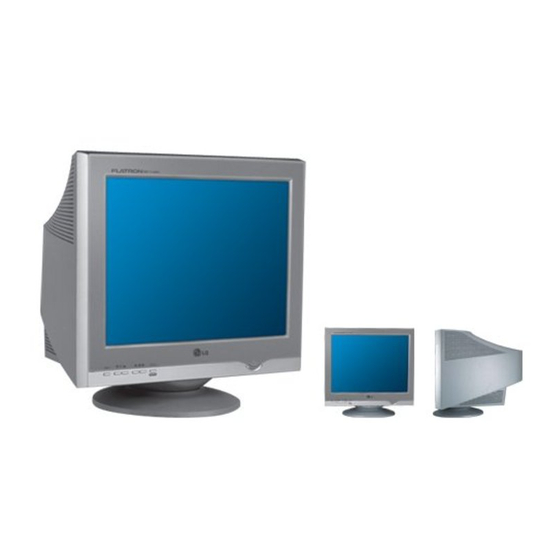
COLOR MONITOR
SERVICE MANUAL
CHASSIS NO. : CA-136
MODEL:
(
) **Same model for Service
CAUTION
BEFORE SERVICING THE UNIT,
READ THE SAFETY PRECAUTIONS IN THIS MANUAL.
Website:http://biz.LGservice.com
E-mail:http://www.LGEservice.com/techsup.html
T730BH(K)
(T730BHKL-K***E*)
(T730SHKL-K***E*)
T730SH(K)
*Same looking with new chassis.
Advertisement
Table of Contents

Related Manuals for LG Flatron T730BH


Summary of Contents for LG Flatron T730BH
-
Page 1: Color Monitor
COLOR MONITOR SERVICE MANUAL CHASSIS NO. : CA-136 MODEL: ) **Same model for Service CAUTION BEFORE SERVICING THE UNIT, READ THE SAFETY PRECAUTIONS IN THIS MANUAL. Website:http://biz.LGservice.com E-mail:http://www.LGEservice.com/techsup.html T730BH(K) (T730BHKL-K***E*) (T730SHKL-K***E*) T730SH(K) *Same looking with new chassis. -
Page 2: Table Of Contents
SPECIFICATIONS ... 2 SAFETY PRECAUTIONS ... 3 SERVICE PRECAUTION... 4 TIMING CHART ... 7 WIRING DIAGRAM ... 9 DISASSEMBLY ... 8 BLOCK DIAGRAM ... 10 1. PICTURE TUBE Size : 17 inch DefIection Angle : 90¡ Neck Diameter : 29.1 mm Stripe Pitch : 0.25 mm Face Treatment... -
Page 3: Safety Precautions
SAFETY-RELATED COMPONENT WARNING! There are special components used in this color monitor which are important for safety. These parts are marked on the schematic diagram and the replacement parts list. It is essential that these critical parts should be replaced with the manufacturer's specified parts to prevent X-radiation, shock, fire, or other hazards. -
Page 4: Service Precaution
CAUTION: Before servicing receivers covered by this service manual and its supplements and addenda, read and follow the SAFETY PRECAUTIONS on page 3 of this publication. NOTE: If unforeseen circumstances create conflict between the following servicing precautions and any of the safety precautions on page 3 of this publication, always follow the safety precautions. - Page 5 General Soldering Guidelines 1. Use a grounded-tip, low-wattage soldering iron and appropriate tip size and shape that will maintain tip temperature within the range or 500 F to 600 F. 2. Use an appropriate gauge of RMA resin-core solder composed of 60 parts tin/40 parts lead. 3.
- Page 6 Circuit Board Foil Repair Excessive heat applied to the copper foil of any printed circuit board will weaken the adhesive that bonds the foil to the circuit board causing the foil to separate from or "lift-off" the board. The following guidelines and procedures should be followed whenever this condition is encountered.
-
Page 7: Timing Chart
Video Sync << Dot Clock (MHz), Horizontal Frequency (kHz), Vertical Frequency (Hz), Horizontal etc... (µs), Vertical etc... (ms) >> Sync Active Time Mode Frequency Sort Polarity 37.50 26.67 74.99 13.335 46.88 21.33 75.01 13.331 53.68 18.63 85.07 11.755 68.677 14.561 85.00 11.764 60.289... -
Page 8: Disassembly
1. T IL T /S WIV E L & B A C K C OV E R R E MOV A L 1) S et the monitor face downward. 2) C arefully remove the T ilt/S wivel by pulling it upward. 3) Remove the screw (b), B ack cover by pus hing it upward. -
Page 9: Wiring Diagram
WIRING DIAGRAM P220 P203 P201 P202 P405 P501 P904 P702 S + S P402 Socket P902 Signal Cable P302 P301 P701... -
Page 10: Block Diagram
BLOCK DIAGRAM Dynamic Focus Static Focus Screen - 1 0 -... -
Page 11: Description Of Block Diagram
DESCRIPTION OF BLOCK DIAGRAM 1. SMPS(Switching Mode Power Supply) When you turn on the power switch, the operating fprocedure is as follows: 1) The AC line voltage is rectified by the bridge diode D900. 2) The control IC(IC901) starts switching and generates switch pulse in the primary turn of the SMPS transformer(T901) 3) The switching pulses of the primary turns are induced... - Page 12 15. Video Pre-Amp Circuit. This circuit amplifies the analog video signal from 0~0.7 V to 0~4 V. It is operated by taking the clamp, R,G,B drive and contrast signal from the MICOM (IC401) 16. Video Output Amp Circuit. This circuit amplifies the video signal which comes from the video pre-amp circuit and amplified it to applied the CDT cathode - 12 -...
-
Page 13: Adjustment
1. Preparation for Service Adjustment GENERAL INFORMATION All adjustment are thoroughly checked and corrected when the monitor leaves the factory, but sometimes several adjustments may be required. Adjustment should be following procedure and after warming up for a minimum of 30 minutes. •... - Page 14 4. Distortion Scanning frequency : All Mode (Mode 1~4) Display image : Crosshatch pattern Horizontal : 10 Row Vertical : 8 Row 2.0mm, 2.0mm 2.0mm, 2.0mm 5. Displa Size drift 4mm : 25 Standard, 10 0.5mm : 180V ~ 264V 6.
- Page 15 11-2. Adjustment of White Balance After finishing adjustment of cut off (back raster), approve "Color(15.0) Full white pattern". Adjust BDRV Data = 85 SCON=127. Adjust RDRV and GDRV to set chromaticity diagram at : x: 0.283 0.005 y: 0.298 0.005 Approve "Window pattern (70x70mm)"...
- Page 16 3. Adjustment Using Service software Program (Adjustment Program) 1. Adjustment for Factory Mode (Preset Mode). 1) Display cross hatch pattern at Mode All. 2) Run alignment program for T730BHKL/T730SHKL on the IBM compatible PC. 3) EEPROM → ALL CLEAR → Y(Yes) command. <Caution>...
- Page 17 4. EDID Data Edit Using Service software Program 4.1 Read and Modify EDID Data 1) Connector the monitor and adjust device as Figure1 2) Display color 15,0 cross hatch pattern at Mode 4. 3) Use EDIT – MODEL SEL. command to select the right model info file. 4) Use EDIT –...
- Page 18 VIDEO SIGNAL GENERATOR Figure 1. Cable Connection Figure 1. Cable Connection Compatible PC - 18 - PARALLEL PORT Power inlet (required) Power Select Switch (110V/220V) Power LED ST Switch V-Sync On/Off Switch (Switch must be ON.) - 18 - 4.7K 4.7K 74LS06 4.7K...
-
Page 19: Troubleshooting Guide
NO POWER (POWER INDICATOR OFF) CHECK FUSE OK?(F901) CHECK D900 BRIDGE DIODE? CHECK C908(+) VOLTAGE 145VDC at 110V input 310VDC at 220V input IC901, Q901 CHECK D971, D961, D951, D904 D941, D942, D906 ? TROUBLE IN Q951, Q952, Q941, Q942, Waveforms Q901, Drain TROUBLESHOOTING GUIDE... - Page 20 NO CHARACTER CHECK IC302 PIN 5,6,7 CHECK IC302 PIN 1, 24, 23, 19, 20, 21 PIN 18 (5V) ? CHECK IC303 PIN 1, 2, 3 PIN8 (8V), PIN 4 (80V) ? CHECK R, G, B CATHODE VOLTAGE? TROUBLE IN CDT SOCKET Waveforms IC302, #5, 6, 7 IC302, #23...
- Page 21 NO VIDEO (POWER INDICATOR GREEN or FLASH) CHECK POWER INDICATOR GREEN or FLASH ? GREEN CHECK SCREEN CONTROL KNOB OF FBT CHECK VOLTAGE AT D961 CATHODE (50V) D971 CATHODE (80V) D951 CATHODE (13V) D941 CATHODE (6.3V)? CHECK IC401 (MICOM) PIN 16 5V (HIGH), IC401 PIN 18 PIN20, PIN21 TROUBLE IN...
-
Page 22: No Vertical Deflection
NO V-DEFLECTION (ONE HORIZONTAL LINE) CHECK IC601 Pin 3 (13V) ? CHECK IC601 PIN 7 (45V)? CHECK IC401 PIN 33, 34 (SAWTOOTH WAVE)? TROUBLE IN IC601, V-CIRCUIT Waveforms IC401, #33 4. NO VERTICAL DEFLECTION IC401, #34 - 22 - TROUBLE IN T901 13V Line TROUBLE IN T701 40V line... - Page 23 Stand-by/SUSPEND/ DPMS OFF MODE FAILURE CHECK IC401 (MICOM) PIN 52, 53 (H/V INPUT) SIGNAL? NO H/V SYNC SIGNAL CHECK IC401 PIN 45, 46 WAVEFORM? CHECK IC401 PIN 16 (5V, HIGH)? CHECK IC401 PIN , 50 ? CHECK Q941,Q951 Q942,Q952 TROUBLE IN T901 or PC Waveforms C401, #45...
-
Page 24: No Degaussing
6. NO DEGAUSSING NO DEGAUSSING CHECK IC401 PIN 4 (5V)? CHECK Q953 COLLECTOR VOLTAGE (0.5V)? CHECK P902? CHECK RL901? TROUBLE IN TH901, DEGAUSSING COIL TROUBLE IN IC401 (MICOM) TROUBLE IN D953 TROUBLE IN P902 TROUBLE IN RL901 - 24 -... - Page 25 IC401 Pin 18 waveform is right? Q719 drain waveform is right? Q705 drain waveform is right? Q706 base, collector waveforms are right? Check if DC voltage of IC401 PIN 35 wave is Variable. Waveforms IC401, #18 Q706, Base 7. H_Deflection Failure 8.
-
Page 26: Trouble In H-Linearity
9. TROUBLE IN H-LINEARITY UNBALANCED OF H-LIN. CHECK IC401 PIN 11, 12,13 CHECK Q711~Q716? CHECK L703? TROUBLE IN C722, C723, C726, C729 TROUBLE IN IC401 (MICOM) TROUBLE IN Q711 ~ Q716 TROUBLE IN L703 Cs SIGNAL TABLE HORIZONTAL FREQUENCY(fH) 30K ~ 33.9K 34K ~ 38.9K 39K ~ 43.9K 44K ~ 48.9K... - Page 27 The Voltage waveform Q706 Collector is right? T701 pin 2 voltage is change with H frequency? Check if AC Voltage of IC401 Pin 35 waveform is Variable Replace IC401. Waveforms Q706, Collector 10. Abnormal H_Size 11. Side Pin or Trap Failure 12.
- Page 28 Check tilt connector connection IC401 Pin 26 output duty varies with different DAC values? Q501 Emitter output varies with different DAC values? Check and replace CRT. IC401 Pin 33, 34 output varies with different DAC values? Check and replace IC401 and IC601.
-
Page 29: High Voltage Failure
Q719 drain waveform is right? Q706 collecter waveform is right? Replace T701 Waveforms Q719, Drain Input full white pattern to monitor. IC302 Pin22 input exists and varies with different patterns? Check P302, D801, R801~803, R798. T701 Pin 6 Voltage exists? Check and replace CRT 15. - Page 30 IC401 Pin 24 output are right? Q710 and parts around are right? Some parts around T701 are right? Check the connection between FBT Pin 12, CRT Socket PCB. Waveforms IC401, #24 17. Focus Failure FBT, #12 - 30 - Check and replace IC401. Replace failed part.
-
Page 31: Micom Failure
IC401 Pin 16 input is over 4.2V? IC401 Pin 45 and 46 inputs are right? IC401 Pin 23 input is High Active? All in/output values are right? Done. Waveforms IC401, #45 Change IC302 18. Micom Failure IC401, #46 19. OSD Failure - 31 - Check Q903,D908,ZD902 Check X401... -
Page 32: Missing Color
20. User Control Failure Check connector Ass’y. IC401 Pins 27 and 28 inputs are right at each function? Check and replace IC401. Done. 21. Missing Color Proper Video levels are on P301 Pin 1, 3 and 5. Proper AC voltage are on all cathodes? Proper DC voltage are on all cathodes? -
Page 33: Purity Failure
22. Visible Retrace Check white balance adjustment. G2 voltage is right? Blank pedestal is on Pin 19, 20 and 21 of IC302 Is V_FLB and DC_bias on G1 Pin at CRT socket? Done. 23. Purity Failure Degaussing Purity is right? Degaussing circuit is right? Replace CRT and verify purity. -
Page 34: Poor Focus
24. Misconvergence Degauss the CDT Adjust Pole4,Pole6 to improve the misconvergence Change CRT and readjust convergence. Done. 25. Poor Focus Adjust focus VR. Improved focus? Check focus leads from FBT to CRT Socket. Check the CRT Socket. Dynamic focus circuit is right? Replace the CRT and verify focus. - Page 35 - 35 -...
-
Page 36: Exploded View
CABINET ASSEMBLY, T730BHKL BRAND C097A PC+ABS TCO99 B/VIEW MOU4.0 BLACK 3091TKC130S CABINET ASSEMBLY, T730SHKL BRAND C097 BLACK B/VIEW MPRII MOU4.0 CDT(CIRC), M41QEE903X 21 NDDP LG-PHILIPS 85KHZ 29.1MM FCDT TCO PLUS (T730BHKL) 6318L17023A CDT(CIRC), M41QEE903X 21 SDDP LG-PHILIPS 85KHZ 29.1MM FCDT TCO PLUS (T730BHKL) 6318L17023E CDT(CIRC), M41QEE903X 21 KDDP LG-PHILIPS 85KHZ 29.1MM FCDT TCO PLUS (T730SHKL) -
Page 37: Replacement Parts List
CAUTION: BEFORE REPLACING ANY OF THESE COMPONENTS, READ CAREFULLY THE SAFETY PRECAUTIONS IN THIS MANUAL. * NOTE : S SAFETY Mark AL ALTERNATIVE PARTS MODEL :T730BHKL DATE:2004.12.20 LOC NO PART NO. DESCRIPTION/SPECIFICATON C A P A C I T O R s C 3 0 1 0 C Q 1 0 2 1 N 4 0 9 0.001UF D 100V 5% PE TP5... - Page 38 MODEL :T730BHKL DATE:2004.12.20 PART NO. DESCRIPTION/SPECIFICATON LOC NO C 9 1 3 0 C E 4 7 6 C K 6 3 8 "47UF SHL,SD 50V M FM5 TP 5" C 9 1 4 0 C Z Z T F T 0 0 1 P ECQB1H153JM3 153J 50V TP5.0 M A T S U S H I T A C 9 1 5...
- Page 39 MODEL :T730BHKL DATE:2004.12.20 PART NO. DESCRIPTION/SPECIFICATON LOC NO 5.6BV 5MA PF Z D 4 0 6 0 D Z P T 5 6 0 0 9 A UZ-5.6BSB PCTRONIX TP52 DO34 500MW 5.6BV 5MA PF Z D 9 0 2 0 D Z P T 5 1 0 0 9 A UZ-5.1BSB PCTRONIX TP DO34 500MW 5.1BV 5MA PF...
- Page 40 MODEL :T730BHKL DATE:2004.12.20 LOC NO PART NO. DESCRIPTION/SPECIFICATON R 4 1 9 0 R N 4 7 0 2 F 4 0 9 47K 1/6W 1% TA52 R 4 2 0 0 R D 2 0 0 1 Q 6 0 9 2K 1/4W(3 5% TA52 R 4 2 1 0 R D 1 5 0 1 Q 6 0 9...
- Page 41 MODEL :T730BHKL DATE:2004.12.20 PART NO. DESCRIPTION/SPECIFICATON LOC NO 10.0MM NI PLATED P 9 0 2 3 6 6 - 1 6 4 A YW396-03AV YEONHO 3P 3.96MM S/T R L 9 0 1 6 9 2 0 T B B 0 0 7 A JZC-42012-2HS HONGMEI 250VAC 5A 12V 2A NO VENTING S C 3 0 1...
- Page 42 CAUTION: BEFORE REPLACING ANY OF THESE COMPONENTS, READ CAREFULLY THE SAFETY PRECAUTIONS IN THIS MANUAL. * NOTE : S SAFETY Mark AL ALTERNATIVE PARTS MODEL :T730SHKL PART NO. DESCRIPTION/SPECIFICATON LOC NO C A P A C I T O R s C 3 0 1 0 C Q 1 0 2 1 N 4 1 9 1000P 100V J POLY NI TP...
- Page 43 MODEL :T730SHKL DATE:2004.12.20 PART NO. DESCRIPTION/SPECIFICATON LOC NO C 9 1 0 0 C K Z T T A 0 0 2 A 220PF K 1KV R TP5.0 C 9 1 1 0 C E 4 7 5 C K 6 3 8 "4.7UF SHL,SD 50V M FM5 TP 5"...
- Page 44 MODEL :T730SHKL PART NO. DESCRIPTION/SPECIFICATON LOC NO C O I L s & C O R E s F B 3 0 2 6 2 1 0 T C E 0 0 3 L BAS3580T BO SUNG 3580MM AXIAL52MM F B 3 0 5 6 2 1 0 T C E 0 0 3 P BRS2550B BO SUNG 2550MM RADIAL F B 3 0 6...
- Page 45 MODEL :T730SHKL DATE:2004.12.20 LOC NO PART NO. DESCRIPTION/SPECIFICATON R 4 2 4 0 R D 1 0 0 0 Q 6 0 9 100 1/4W(3 5% TA52 R 4 2 5 0 R D 1 0 0 0 Q 6 0 9 100 1/4W(3 5% TA52 R 4 2 6 0 R D 1 0 0 0 Q 6 0 9...
- Page 46 MODEL :T730SHKL DATE:2004.12.20 PART NO. DESCRIPTION/SPECIFICATON LOC NO S C 9 0 1 6 6 2 0 T K B 0 0 2 B SA-4S HUA JIE AC UNIVERSAL 3PIN B L A C K S G 3 0 5 6 9 1 8 T R T 0 0 5 A "SSG-102-A0,1KV SMART RADIAL TAPING"...
-
Page 49: Printed Circuit Board
Dec 2004 P/NO : 3828TSL109G Printed in China...
Need help?
Do you have a question about the Flatron T730BH and is the answer not in the manual?
Questions and answers