Advertisement

Quick Links

ICD-BP100/BP120
SERVICE MANUAL
Ver 1.1 2002. 07
Sony Corporation
9-873-072-12
2002G1600-1
Personal Audio Company
© 2002.07
Published by Sony Engineering Corporation
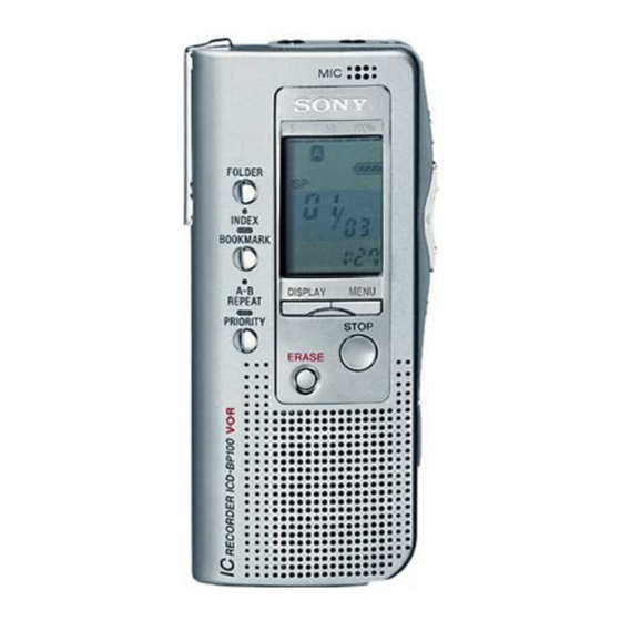
Photo : ICD-BP100
SPECIFICATIONS
Recording media
Built-in flash memory, Monaural recording
Recording time
ICD-BP100: SP: 63 minutes, LP: 168 minutes
ICD-BP120: SP: 127 minutes, LP: 339 minutes
Frequency response
SP: 250 Hz - 7,300 Hz
LP: 300 Hz - 3,500 Hz
Speaker
approx. 3.2 cm (1
Power output
300 mW
Input/Output
• Earphone jack (minijack) for 16 - 300 ohms
earphone/headphones
• Microphone jack (minijack, monaural)
Plug in power
Minimum input level 0.6 mV
3 kilohms or lower impedance microphone
• USB connector
Playback speed control
FAST +30%, SLOW –15%
Power requirements
Two LR03 (size AAA) alkaline batteries: 3 V DC
Dimensions (w/h/d) (not incl. projecting parts and controls)
44.5 × 105.3 × 14.0 mm (1
Mass (incl. batteries)
79 g (2.79 oz)
Earphone × 1
Supplied accessories
Carrying case × 1
LR03 (size AAA) alkaline battery × 2 (U.S.A. model
only)
Connecting cable × 1 (ICD-BP100 only)
"Digital Voice Editor" (CD-ROM) × 1
Registration card × 1 (U.S.A. and European models
only)
Optional accessories
Electret Condenser Microphone ECM-Z60, ECM-
T115
Earphone MDR-ED228LP, MDR-E818LP
Connecting cord RK-G64
Your dealer may not handle some of the above listed optional accessories. Please
ask the dealer for detailed information.
Design and specifications are subject to change without notice.
Canadian Model
/
in.) dia.
5
16
× 4
×
/
/
/
in.)
13
1
9
16
4
16
US Model
ICD-BP100/BP120
AEP Model
UK Model
E Model
ICD-BP100
Tourist Model
ICD-BP100/BP120
IC RECORDER

Advertisement

Table of Contents
loading

Summary of Contents for Sony ICD-BP100

  • Page 1 Photo : ICD-BP100 SPECIFICATIONS Recording media Built-in flash memory, Monaural recording Recording time ICD-BP100: SP: 63 minutes, LP: 168 minutes ICD-BP120: SP: 127 minutes, LP: 339 minutes Frequency response SP: 250 Hz - 7,300 Hz LP: 300 Hz - 3,500 Hz Speaker approx.
  • Page 2: Table Of Contents

    ICD-BP100/BP120 TABLE OF CONTENTS 1. GENERAL ·································································· 3 Flexible Circuit Board Repairing • Keep the temperature of the soldering iron around 270°C during repairing. 2. DISASSEMBLY • Do not touch the soldering iron on the same conductor of the 2-1. Sub Block Assy, Upper Lid ············································· 4 circuit board (within 3 times).
  • Page 3: General

    ICD-BP100/BP120 SECTION 1 GENERAL This section is extracted from instruction manual. Main unit Rear 1 MIC (built-in microphone) qf zREC (record) /STOP wa PLAY SPEED selector (18) ws MIC SENS (microphone (12) button (13, 24) sensitivity) selector (14) 2 Display window (64)
  • Page 4: Disassembly

    ICD-BP100/BP120 SECTION 2 DISASSEMBLY Disassemble the unit in the order as shown below. F-SW board MAIN board, P-SW board PC board Sub block assy,upper lid Note : Follow the disassembly procedure in the numerical order given. 2-1. SUB BLOCK ASSY, UPPER LID...
  • Page 5: Main Board, P-Sw Board

    ICD-BP100/BP120 2-3. MAIN BOARD, P-SW BOARD 1 screw (1.7 × 4) 4 Main board 5 Remove the soldering 6 P-SW board 2 connector (CN802) claw case assy claw 2-4. PC BOARD 1 screw (1.7 × 4) 3 PC board case assy...
  • Page 6: Diagrams

    ICD-BP100/BP120 SECTION 3 DIAGRAMS Note on Schematic Diagrams: WAVEFORMS • All capacitors are in µF unless otherwise noted. pF: µµF 50 WV or less are not indicated except for electrolytics IC712 od XTAL and tantalums. • All resistors are in Ω and W or less unless otherwise specified.
  • Page 7: Block Diagram

    ICD-BP100/BP120 3-1. BLOCK DIAGRAM MIC101 IC101 IC102 MAIN BOARD IC107 IC112 MIC AMP ALC AMP A/D, D/A CONVERTER Q105 AVCC RV101 IC110 BUFFER POWER AMP VIN+ wVOL J101 VOUT VIN- VOUT VOUT SP101 VIN- IC103 (SPEAKER) VOR CONTROL PDWN (PLUG IN POWER)
  • Page 8: Printed Wiring Board - Main Section (1/2)

    ICD-BP100/BP120 3-2. PRINTED WIRING BOARD – MAIN SECTION (1/2) – • : Uses unleaded solder. * Replacement of IC109 used in this set requires a special tool. MAIN BOARD (SIDE A) PC BOARD (Page 16) Q102 J101 (PLUG IN POWER)
  • Page 9: Printed Wiring Board - Main Section (2/2)

    ICD-BP100/BP120 3-3. PRINTED WIRING BOARD – MAIN SECTION (2/2) – • : Uses unleaded solder. TO LCD F-SW BOARD (Page 15) MAIN BOARD (SIDE B) CN702 IC 715 SP101 (SPEAKER) MIC101 BP100 IC 712 IC 716 IC 706 R772 C726...
  • Page 10: Schematic Diagram - Main Section (1/3)

    ICD-BP100/BP120 3-4. SCHEMATIC DIAGRAM – MAIN SECTION (1/3) – • Refer to page 22 for IC Block Diagrams. IC B/D IC B/D IC B/D IC B/D IC B/D IC B/D...
  • Page 11: Schematic Diagram - Main Section (2/3)

    ICD-BP100/BP120 3-5. SCHEMATIC DIAGRAM – MAIN SECTION (2/3) – • Refer to page 20 for IC Block Diagrams. • Refer to page 21 for IC Pin Function. • Refer to page 6 for Waveforms.
  • Page 12: Schematic Diagram - Main Section (3/3)

    ICD-BP100/BP120 3-6. SCHEMATIC DIAGRAM – MAIN SECTION (3/3) – • Refer to page 20 for IC Block Diagrams. IC B/D IC B/D IC B/D...
  • Page 13: Schematic Diagram - F-Sw Section

    ICD-BP100/BP120 3-7. SCHEMATIC DIAGRAM – F-SW SECTION – A-B REPEAT INDEX/ /PRIORITY BOOKMARK DISPLAY FOLDER STOP ERASE MENU (3/3) (Page 12) R520 470k R522 0 R518...
  • Page 14: Printed Wiring Board - F-Sw Section (1/2)

    ICD-BP100/BP120 3-8. PRINTED WIRING BOARD – F-SW SECTION (1/2) – • : Uses unleaded solder. F-SW BOARD (SIDE A) A-B REPEAT /PRIORITY INDEX/ FOLDER BOOKMARK 1-680-351- DISPLAY ERASE (12) IC 507 STOP MENU • Semiconductor Location Ref. No. Location IC507...
  • Page 15: Printed Wiring Board - F-Sw Section (2/2)

    ICD-BP100/BP120 3-9. PRINTED WIRING BOARD – F-SW SECTION (2/2) – • : Uses unleaded solder. F-SW BOARD (SIDE B) R522 (BACK LIGHT) R518 IC 504 • Semiconductor Location Ref. No. Location D501 F-14 D502 D-16 D503 G-17 1-680-351- D701 F-12...
  • Page 16: Printed Wiring Board - Pc Section

    ICD-BP100/BP120 3-10. PRINTED WIRING BOARD – PC SECTION – • : Uses unleaded solder. • Semiconductor Location Ref. No. Location PC BOARD PC BOARD (SIDE A) (SIDE B) IC801 IC802 S701 IC803 PLAY SPEED SLOW NORMAL FAST Q801 Q802 S101...
  • Page 17: Schematic Diagram - Pc Section

    ICD-BP100/BP120 3-11. SCHEMATIC DIAGRAM – PC SECTION – (1/3) (Page 10) PLAY SPEED MIC SENS SLOW NORMAL FAST...
  • Page 18: Printed Wiring Board - P-Sw Section

    ICD-BP100/BP120 3-12. PRINTED WIRING BOARD – P-SW SECTION – • : Uses unleaded solder. P-SW BOARD (SIDE A) HOLD. 1-680-352- (12) MAIN BOARD MAIN BOARD (Page 9) (Page 9) (12) 1-680-352- P-SW BOARD (SIDE B)
  • Page 19: Schematic Diagram - P-Sw Section

    ICD-BP100/BP120 3-13. SCHEMATIC DIAGRAM – P-SW SECTION – HOLD . (3/3) (Page 12)
  • Page 20: Ic Block Diagrams

    ICD-BP100/BP120 3-14. IC BLOCK DIAGRAMS IC111 NJM2772V(TE2) (MAIN BOARD) IC715 BU2090FS-E2 (MAIN BOARD) IC102 AN6123MS-TXL (MAIN BOARD) STBY 16 15 14 13 12 11 PA-A OUTA 12 BIT CONTROL SHIFT CIRCUIT REGISTER CENTER SW OUTPUT 12 BIT BUFFER PA-C VREF...
  • Page 21: Ic Pin Function Description

    ICD-BP100/BP120 3-15. IC PIN FUNCTION DESCRIPTION • IC712 MB90F523APF-G-116-BND (SYSTEM CONTROL) Pin No. Pin Name Description RTC CE Real time clock chip enable signal output. BEEP Beep signal output. XFLMRE Flash memory read enable signal output. XFLMWE Flash memory write enable signal output.
  • Page 22 ICD-BP100/BP120 Pin No. Pin Name Description XHSTBY Hardware standby signal input. Operation mode input terminal 2. Operation mode input terminal 1 (connected to VCC). Operation mode input terminal 0. XRESET Reset input terminal. – Ground terminal. XTALIN Main oscillator input terminal (4.096MHz).
  • Page 23: Exploded Views

    ICD-BP100/BP120 SECTION 4 EXPLODED VIEWS NOTE: • -XX, -X mean standardized parts, so they may • The mechanical parts with no reference number have some differences from the original one. in the exploded views are not supplied. • Items marked “*” are not stocked since they •...
  • Page 24: Main Board Section

    ICD-BP100/BP120 4-2. MAIN BOARD SECTION supplied Ref. No. Part No. Description Remarks Ref. No. Part No. Description Remarks * 51 A-3347-064-A PC BOARD, COMPLETE 3-224-515-01 PLATE, LIGHT GUIDE 3-224-518-01 GUIDE (PC) 3-229-218-01 SHEET (SD-S) * 53 A-3323-660-A MAIN BOARD, COMPLETE (BP120)
  • Page 25: Electrical Parts List

    ICD-BP100/BP120 SECTION 5 F-SW MAIN ELECTRICAL PARTS LIST NOTE: • Due to standardization, replacements in the • CAPACITORS: • SEMICONDUCTORS uF: µF In each case, u: µ, for example: parts list may be different from the parts uA...: µA... , uPA... , µPA... , specified in the diagrams or the components •...
  • Page 26 ICD-BP100/BP120 MAIN Ref. No. Part No. Description Remarks Ref. No. Part No. Description Remarks C106 1-115-467-11 CERAMIC CHIP 0.22uF 10.00% 10V C170 1-125-837-11 CERAMIC CHIP 6.3V C107 1-164-931-11 CERAMIC CHIP 100PF 10.00% 16V C171 1-125-777-11 CERAMIC CHIP 0.1uF 10.00% 10V...
  • Page 27 ICD-BP100/BP120 MAIN Ref. No. Part No. Description Remarks Ref. No. Part No. Description Remarks IC111 8-759-826-02 IC NJM2772V(TE2) R148 1-218-990-11 SHORT IC112 8-759-677-71 IC LMV751M5X R149 1-218-985-11 RES-CHIP 470K 1/16W IC706 8-759-495-18 IC TC58V64AFT (BP100) R150 1-218-985-11 RES-CHIP 470K 1/16W...
  • Page 28 ICD-BP100/BP120 MAIN P-SW Ref. No. Part No. Description Remarks Ref. No. Part No. Description Remarks R760 1-218-965-11 RES-CHIP 1/16W < TRANSISTOR > R763 1-218-953-11 RES-CHIP 1/16W R764 1-218-981-11 RES-CHIP 220K 1/16W Q801 8-729-420-29 TRANSISTOR 2SD1819A R765 1-218-977-11 RES-CHIP 100K 1/16W...
  • Page 29 ICD-BP100/BP120 Ref. No. Part No. Description Remarks Ref. No. Part No. Description Remarks MISCELLANEOUS 3-229-038-11 MANUAL, INSTRUCTION (ENGLISH)(BP100) 3-229-038-21 MANUAL, INSTRUCTION ************** (FRENCH)(BP100:Canadian,AEP) 1-694-773-11 CONDUCTIVE BOARD, CONNECTION 3-229-038-31 MANUAL, INSTRUCTION 1-804-254-11 DISPLAY PANEL, LIQUID CRYSTAL (SPANISH)(BP100:AEP,E) SP101 1-529-901-11 SPEAKER (32mm)
  • Page 30 ICD-BP100/BP120 MEMO...
  • Page 31 TP512 of the F-SW board with a jumper. Then the guaranteed. The resultant information of this check is unit enters the Model Code Writing mode. When the unit is ICD-BP100, press the > switch. When stored in the TOC-AREA so that the BAD BLOCK area should not be used.
  • Page 32 ICD-BP100/BP120 REVISION HISTORY Clicking the version allows you to jump to the revised page. Also, clicking the version at the upper right on the revised page allows you to jump to the next revised page. Ver. Date Description of Revision 2001.03...

This manual is also suitable for:

Icd-bp120

Table of Contents