Sony ICD-BM1 Service Manual
Hide thumbs
Also See for ICD-BM1:
- Operating instructions manual (68 pages) ,
- Service manual (44 pages) ,
- Quick reference card (2 pages)
Table of Contents
Advertisement
Quick Links
SERVICE MANUAL
Ver. 1.2 2009.05
Recording media
"Memory Stick", Monaural recording
Recording time
Maximum recording time and number of messages for a "Memory Stick"
The maximum recording time for all the folders and the maximum number
of messages are as follows. You can record messages for the maximum
recording time in a single folder.
4MB
8MB
16MB
ST*
10min.
20min.
40min.
SP**
30min.
1hr
2hr 10min. 4hr 20min. 8hr 50min. 17hr 45min.
LP***
1hr 20min. 2hr 50min. 5hr 45min. 11hr 45min. 23hr 35min. 47hr 25min.
Number
456
950
963
of Messages
*ST:
High quality recording mode
(stereo sound with an external stereo microphone not supplied)
**SP: Standard play recording mode (monaural sound)
***LP: Long play recording mode (monaural sound)
Frequency range
ST: 60 Hz - 13,500 Hz
SP: 60 Hz - 7,000 Hz
LP: 80 Hz - 3,500 Hz
Speaker
approx. 28 mm (
Power output
350 mW
Sony Corporation
9-887-675-03
Audio&Video Business Group
2009E04-1
Published by Sony Techno Create Corporation
© 2009.05
ICD-BM1/BM1A/BM1AVTP/
SPECIFICATIONS
32MB
64MB
128MB
1hr 25min. 2hr 50min. 5hr 50min.
1,016
1,016
1,016
(hr: hours /min.: minutes)
in.) dia.
29/32
BM1B/BM1DR9
ICD-BM1A/BM1AVTP/BM1B/BM1DR9
Input/Output
• Earphone jack (minijack) for 8 - 300 ohms ear
receiver/headphones
• Microphone jack (minijack, stereo)
Plug in power
Minimum input level: 0.7 mV 3 kilohms or
lower impedance microphone
• USB connector
• DC IN 3V jack
Playback speed control +100% to -50% (DPC)
Power requirements
Two size AAA (LR03) alkaline batteries: 3 V DC
Dimensions
36.6 × 112.3 × 21mm (1
(w/h/d) (not incl. projecting parts and controls)
Mass
98 g (3.5 oz) (incl. batteries and a "Memory Stick")
Supplied accessories
"Memory Stick" × 1 (ICD-BM1A/BM1AVTP only)
"Memory Stick Duo" (with an adaptor) × 1
(ICD-BM1/BM1B/BM1DR9 only)
"Digital Voice Editor" (CD-ROM) × 1
"Dragon NaturallySpeaking" (CD-ROM) × 1
(ICD-BM1AVTP only)
Ear receiver × 1
USB connecting cable × 1
Carrying case × 1
Clamp filter × 1
Design and specifications are subject to change without notice.
US Model
AEP Model
ICD-BM1
× 4
×
in.)
1/2
1/2
27/32
IC RECORDER
Advertisement
Table of Contents

Related Manuals for Sony ICD-BM1


Summary of Contents for Sony ICD-BM1
- Page 1 28 mm ( in.) dia. 29/32 Clamp filter × 1 Power output 350 mW Design and specifications are subject to change without notice. IC RECORDER Sony Corporation 9-887-675-03 Audio&Video Business Group 2009E04-1 Published by Sony Techno Create Corporation © 2009.05...
-
Page 2: Table Of Contents
ICD-BM1/BM1A/BM1AVTP/BM1B/BM1DR9 Flexible Circuit Board Repairing TABLE OF CONTENTS • Keep the temperature of the soldering iron around 270 ˚C during repairing. GENERAL • Do not touch the soldering iron on the same conductor of the Index to Parts and Controls ..........3 circuit board (within 3 times). -
Page 3: General
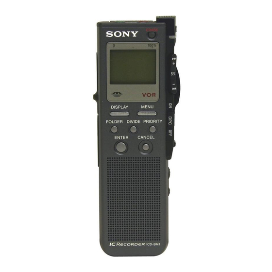
ICD-BM1/BM1A/BM1AVTP/BM1B/BM1DR9 SECTION 1 This section is extracted from instruction manual. GENERAL Rear Index to Parts and Controls Refer to the pages indicated in parentheses for details. Front 1 MIC (microphone) (PLUG qs Built-in microphone (14) wz Memory Stick slot cover (10) -
Page 4: Disassembly
ICD-BM1/BM1A/BM1AVTP/BM1B/BM1DR9 SECTION 2 DISASSEMBLY Note: Disassemble the unit in the order as shown below. 2-1. KNOB (REAR) (Page 4) 2-2. CHASSIS BLOCK ASSY (Page 5) 2-6. CHASSIS SECTION 2-3. SW BOARD (Page 7) (Page 5) 2-4. PLATE (MS) SECTION 2-7. -
Page 5: Chassis Block Assy
ICD-BM1/BM1A/BM1AVTP/BM1B/BM1DR9 2-2. CHASSIS BLOCK ASSY 1 Open the shutter(MS). (broken the switch.) 2 Push the attachment (battery lid) about 5mm. 5 chassis block assy 3 two screws (1.4) 2-3. SW BOARD 0 SW board 8 screw (1.4 × 3) 1 two claws... -
Page 6: Plate (Ms) Section
ICD-BM1/BM1A/BM1AVTP/BM1B/BM1DR9 2-4. PLATE (MS) SECTION 2 precision pan screw (M1.4) (EG) 6 plate (MS) section 5 claw 1 MIC301 3 screw (1.4 × 3) 4 claw 2-5. LCD BOARD qs LCD board 1 screw (self tap) qa EL901 9 holder (LCD) -
Page 7: Chassis Section
ICD-BM1/BM1A/BM1AVTP/BM1B/BM1DR9 2-6. CHASSIS SECTION 1 two claws 6 CN701 7 chassis (rear) section 2 claw 3 claw 4 claw 8 chassis (front) section 2-7. MEMORY STICK CONNECTOR 2 chassis (rear) 1 memory stick connector... -
Page 8: Main Board
ICD-BM1/BM1A/BM1AVTP/BM1B/BM1DR9 2-8. MAIN BOARD 3 MIC301 2 Remove the soldering of MIC301. 4 precision pan screw (M1.4) (EG) 1 Remove the soldering of speaker. 6 MAIN board 5 claw chassis (front) -
Page 9: Diagrams
ICD-BM1/BM1A/BM1AVTP/BM1B/BM1DR9 SECTION 3 DIAGRAMS 3-1. BLOCK DIAGRAM – MAIN Section – IC301 ADC,DAC, IC601 IC701(1/2) MIC301 HEADPHONE AMP DSP (IRIS) CPU (Cliche) (MIC) MEMORY STICK MSDIO J302 SDIO AINR2 STDO ADASI SCLK MSCLK PLUG IN POWER TSCK SCK0 MSBS AINL2... -
Page 10: Block Diagram - Lcd/Sw Section
ICD-BM1/BM1A/BM1AVTP/BM1B/BM1DR9 3-2. BLOCK DIAGRAM – LCD/SW Section – IC701(2/2) IC504 IC501 Q504 CPU (Cliche) +1.6V XRST VOLTAGE DC/DC DETECT SWITCH LCD1 LCDDO CONV. DRY BATTERY LIQUID (Page 9) IC503 LCDSCK CRYSTAL IVDD XLCDCS VOLTAGE DISPLAY (IC601) XLCDRST DETECT MODULE S908,954,957... - Page 11 ICD-BM1/BM1A/BM1AVTP/BM1B/BM1DR9 • Waveforms THIS NOTE IS COMMON FOR PRINTED WIRING BOARDS AND SCHEMATIC DIAGRAMS. (In addition to this, the necessary note is IC801 qd (XOUT) printed in each block.) Common Note on Schematic Diagrams: • All capacitors are in µF unless otherwise noted. (p: pF) 2.1Vp-p...
-
Page 12: Printed Wiring Board - Main Section
ICD-BM1/BM1A/BM1AVTP/BM1B/BM1DR9 3-3. PRINTED WIRING BOARD – MAIN Section – : Uses unleaded solder. J501 MEMORY DC IN 3V STICK MAIN BOARD (SIDE A) TP801 • Semiconductor TP701 TP702 Location Q704 TP708 R106 C303 C108 R722 R760 CN701 D502 Ref. No. -
Page 13: Schematic Diagram - Main Section (1/3)
ICD-BM1/BM1A/BM1AVTP/BM1B/BM1DR9 • Refer to page 11 for Waveform. 3-4. SCHEMATIC DIAGRAM – MAIN Section (1/3) – • Refer to page 19 for IC Block Diagrams. IC505 C803 C804 C805 R818 X801 R101 R102 R819 TP101 C504 C101 C102 R306 C522... -
Page 14: Schematic Diagram - Main Section (2/3)
ICD-BM1/BM1A/BM1AVTP/BM1B/BM1DR9 • Refer to page 11 for Waveform. 3-5. SCHEMATIC DIAGRAM – MAIN Section (2/3) – • Refer to page 25 for IC Pin Descriptions. Q704 R714 R715 R716 R717 R722 R721 R718 R723 C738 IC702 C718 R702 R319 IC707... -
Page 15: Schematic Diagram - Main Section (3/3)
ICD-BM1/BM1A/BM1AVTP/BM1B/BM1DR9 3-6. SCHEMATIC DIAGRAM – MAIN Section (3/3) – • Refer to page 22 for IC Pin Descriptions. (Page 14) (Page 13) R621 IC602 C603 X601 R614 D503 TP505 L501 R622 R504 C508 R506 R508 C605 RB606 R503 R505 R507... -
Page 16: Schematic Diagram - Lcd/Sw Section
ICD-BM1/BM1A/BM1AVTP/BM1B/BM1DR9 3-7. SCHEMATIC DIAGRAM – LCD/SW Section – D951 CN903 CN951 CN902 R957 R968 R973 Q951 R958 R951 R952 C951 C954 D952 R974 (Page 14) S955 Q952 S961 RB951 R919 S908 R909 R962 R963 R966 R969 R970 R972 CN901 R920... -
Page 17: Printed Wiring Board - Lcd Section
ICD-BM1/BM1A/BM1AVTP/BM1B/BM1DR9 3-8. PRINTED WIRING BOARD – LCD Section – : Uses unleaded solder. LCD BOARD (SIDE A) R919 S905 S908 PRIORITY ERASE R916 S903 S901 MENU CANCEL S907 DIVIDE D901 TP903 R918 EL901 C913 BACK TP902 LIGHT R917 S902 S906... -
Page 18: Printed Wiring Board - Sw Section
ICD-BM1/BM1A/BM1AVTP/BM1B/BM1DR9 3-9. PRINTED WIRING BOARD – SW Section – : Uses unleaded solder. SW BOARD (SIDE A) S956 Q951 S961 (FUNCTION-A) S958 CN951 (OPEN/CLOSE) (FUNCTION-B) 1860-923- S952 S953 S956,958 DIC(L) – CONF(H) (FUNCTION) REC – STOP – PLAY – B.SPACE... - Page 19 ICD-BM1/BM1A/BM1AVTP/BM1B/BM1DR9 • IC Block Diagrams IC301 AK4569VN-L (MAIN Board (1/3)) IPGA & ADC BICK AINL1 AINL2 IPGA MUTET MCLK AINR1 AINR2 MOUT AUDIO I/F LRCK CONTROLLER CDTI BOOST DATT CCLK HP AMP CONTROL REGISTER MOUT VREF VREF VCOM IC703 RX-4591CF (MAIN Board (1/3)) 32.768kHz...
- Page 20 ICD-BM1/BM1A/BM1AVTP/BM1B/BM1DR9 IC704 BU2090FS-E2 (MAIN Board (1/3)) 16 15 14 13 12 11 12 BIT CONTROL SHIFT CIRCUIT REGISTER OUTPUT 12 BIT BUFFER STORAGE (OPEN DRAIN) REGISTER 5 6 7 8 IC705 AK6417CH-E2 (MAIN Board (1/3)) DATA REGISTER R/W AMPS AUTO ERASE...
- Page 21 ICD-BM1/BM1A/BM1AVTP/BM1B/BM1DR9 IC801 M66291GP-2 (MAIN Board (1/3)) CVDD IVDD I/O BLOCK USB-IP OSCILLATION BUFFER /48MHzPLL INTERRUPT CONTROLLER VBUS VBUS INTERFACE TRON INPUT CIRCUIT UNIT TRANSFER ENDPOINT D+ PIN PULLUP (BIU) CONTROLLER CONTROLLER CIRCUIT TEST SERIAL DACK1 INTERFACE FIFO MEMORY CONTROLLER TRANSCEIVER...
- Page 22 ICD-BM1/BM1A/BM1AVTP/BM1B/BM1DR9 • IC Pin Descriptions IC601 µPD77213F1-101-DA2 (DSP) (MAIN BOARD) Pin No. Pin Name Pin Description 1 to 3 — Not used EVDD — I/O power supply (3.0 V) XADACS AD/DA chip select ADACCLK AD/DA clock ADACDTI AD/DA data input...
- Page 23 ICD-BM1/BM1A/BM1AVTP/BM1B/BM1DR9 Pin No. Pin Name Pin Description TSIEN Time sharing serial input enable EVDD — I/O power supply (3.0 V) Memory address bus 1 (Not used) Memory address bus 0 (Not used) — IVDD — Core power supply (1.5 V)
- Page 24 ICD-BM1/BM1A/BM1AVTP/BM1B/BM1DR9 Pin No. Pin Name Pin Description EVDD — I/O power supply (3.0 V) Memory data bus (Not used) MD13 Memory data bus (Not used) MD10 Memory data bus (Not used) MD11 Memory data bus (Not used) Memory data bus (Not used)
- Page 25 ICD-BM1/BM1A/BM1AVTP/BM1B/BM1DR9 IC701 LC67F5006A-F3A15-E (CPU) (MAIN BOARD) Pin No. Pin Name Pin Description — DSPPWR DSP power supply control SRAM output enable, USB read strobe WAKEUP KEY WAKE UP interrupt XDCINDET DC IN detection XUSBIRQ USB driver interrupt request (Not used)
- Page 26 ICD-BM1/BM1A/BM1AVTP/BM1B/BM1DR9 Pin No. Pin Name Pin Description CF oscillator pin — XRST Reset input (L: Reset) XSTBY Standby (L: HW standby) BOOT Boot pin, not used. (set at “L”) 68 to 75 D0_D7 SRAM and USB data bus — 77 to 84...
-
Page 27: Exploded Views
ICD-BM1/BM1A/BM1AVTP/BM1B/BM1DR9 SECTION 4 EXPLODED VIEWS NOTE: • The mechanical parts with no reference • Color Indication of Appearance Parts number in the exploded views are not supplied. Example : • Items marked “*” are not stocked since KNOB, BALANCE (WHITE) ... (RED) they are seldom required for routine service. -
Page 28: Case Section
ICD-BM1/BM1A/BM1AVTP/BM1B/BM1DR9 4-2. CASE SECTION not supplied not supplied not supplied Ref. No. Part No. Description Remark Ref. No. Part No. Description Remark 3-260-497-02 CASE 3-260-506-01 SHEET (ERASE), ADHESIVE 3-260-425-01 NET (SPEAKER) 3-260-435-01 BUTTON (ERASE) 3-260-436-01 BUTTON (VOL) 3-261-295-01 BUTTON (FRONT) (B) -
Page 29: Ornament Section
ICD-BM1/BM1A/BM1AVTP/BM1B/BM1DR9 4-3. ORNAMENT SECTION MIC301 Ref. No. Part No. Description Remark Ref. No. Part No. Description Remark * 101 A-4541-673-A SW BOARD, COMPLETE 3-260-525-01 SPRING (REVIEW), TORSION X-3384-213-1 SLIDE ASSY 3-247-180-01 SCREW (1.4X3) 3-260-481-01 ORNAMENT (MIC) 3-225-996-12 SCREW (M1.4) (EG), PRECISION PAN... -
Page 30: Chassis (1) Section
ICD-BM1/BM1A/BM1AVTP/BM1B/BM1DR9 4-4. CHASSIS (1) SECTION EL901 LCD901 not supplied not supplied SP301 Ref. No. Part No. Description Remark Ref. No. Part No. Description Remark 3-260-479-01 CUSHION (SPEAKER) 3-248-370-01 SCREW, SELF TAP 3-963-156-01 SCREW (BTP1.7X3), SPECIAL * 158 A-4541-671-A LCD BOARD, COMPLETE... -
Page 31: Chassis (2) Section
ICD-BM1/BM1A/BM1AVTP/BM1B/BM1DR9 4-5. CHASSIS (2) SECTION Ref. No. Part No. Description Remark Ref. No. Part No. Description Remark A-1257-416-A MAIN BOARD, COMPLETE 3-221-591-01 NUT (M1.4) 3-225-996-12 SCREW (M1.4) (EG), PRECISION PAN 3-260-489-01 CHASSIS (REAR) 3-260-477-01 TERMINAL (–), BATTERY 3-260-480-01 SHEET (MS), ADHESIVE... -
Page 32: Electrical Parts List
ICD-BM1/BM1A/BM1AVTP/BM1B/BM1DR9 SECTION 5 MAIN ELECTRICAL PARTS LIST NOTE: • Due to standardization, replacements in • Items marked “*” are not stocked since When indicating parts by reference the parts list may be different from the they are seldom required for routine service. - Page 33 ICD-BM1/BM1A/BM1AVTP/BM1B/BM1DR9 MAIN Ref. No. Part No. Description Remark Ref. No. Part No. Description Remark C319 1-125-777-11 CERAMIC CHIP 0.1uF C738 1-125-777-11 CERAMIC CHIP 0.1uF C320 1-125-777-11 CERAMIC CHIP 0.1uF C801 1-125-777-11 CERAMIC CHIP 0.1uF C321 1-125-837-11 CERAMIC CHIP 6.3V C802 1-125-777-11 CERAMIC CHIP 0.1uF...
- Page 34 ICD-BM1/BM1A/BM1AVTP/BM1B/BM1DR9 MAIN Ref. No. Part No. Description Remark Ref. No. Part No. Description Remark IC801 6-702-098-01 IC M66291GP-2 R322 1-218-977-11 RES-CHIP 100K 1/16W R323 1-218-929-11 RES-CHIP 1/16W < JACK > R501 1-218-985-11 RES-CHIP 470K 1/16W R502 1-218-985-11 RES-CHIP 470K 1/16W...
- Page 35 ICD-BM1/BM1A/BM1AVTP/BM1B/BM1DR9 MAIN Ref. No. Part No. Description Remark Ref. No. Part No. Description Remark R760 1-218-965-11 RES-CHIP 1/16W < RESISTOR > R804 1-218-933-11 RES-CHIP 1/16W R807 1-218-933-11 RES-CHIP 1/16W R951 1-218-953-11 RES-CHIP 1/16W R808 1-218-989-11 RES-CHIP 1/16W R952 1-218-953-11 RES-CHIP...
- Page 36 ICD-BM1/BM1A/BM1AVTP/BM1B/BM1DR9 Ver. 1.2 Ref. No. Part No. Description Remark ACCESSORIES ************ 1-543-798-11 FILTER, CLAMP (FERRITE CORE) 1-823-519-31 CORD, CONNECTION (USB) 2-585-846-11 SOFT, APPLICATION (Dragon Naturally Speaking) (ENGLISH) (BM1AVTP) 2-587-484-11 MANUAL, INSTRUCTION (Digital Voice Editor 2) (ENGLISH) (BM1A,BM1AVTP) 2-599-593-11 INSTRUCTION (Dragon Naturally Speaking)
- Page 37 ICD-BM1/BM1A/BM1AVTP/BM1B/BM1DR9 MEMO...
- Page 38 ICD-BM1/BM1A/BM1AVTP/BM1B/BM1DR9 REVISION HISTORY Clicking the version allows you to jump to the revised page. Also, clicking the version at the top of the revised page allows you to jump to the next revised page. Ver. Date Description of Revision 2007.04 2008.03...
Need help?
Do you have a question about the ICD-BM1 and is the answer not in the manual?
Questions and answers