Advertisement
BACK LIGHT LCD
2HD/2DD FLOPPY DISK DRIVE
BASS REFLEX SPEAKER SYSTEM
INDEX
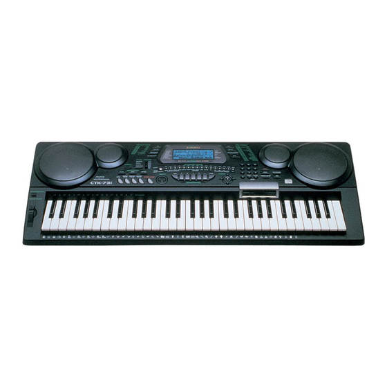
CTK-731
JULY.1999
000-009
8 BEAT
DSP
010-019
16 BEAT
020-029
ROCK
030-039
POPS I
040-049
POPS II
CONTRAST
10 DSP
050-059
JAZZ
0
REVERB 1
060-069
EUROPEAN
1
REVERB 2
070-079
LATIN I
2
REVERB 3
080-089
LATIN II/VARIOUS I
FREE SESSION
3
CHORUS
090-099
VARIOUS II
4
TREMOLO
100-109
USER RHYTHM
5
PHASE SHIFTER
6
ORGAN SPEAKER
ONE TOUCH PRESET
7
ENHANCER
8
FLANGER
9
EQ LOUDNESS
MUSICAL INFOMATION SYSTEM
FULL RANGE
MAX
CHORD
FINGERED
CASIO CHORD
MIN
RECORD
SONG
PATTERN
NORMAL/
VARIATION/
SYNCHRO/
INTRO
FILL-IN
FILL-IN
ENDING
GM SOUND KEYBOARD
TONE
000-007
PIANO
008-015
CHROMATIC PERC
016-023
ORGAN
024-031
GUITAR
RHYTHM
032-039
BASS
040-047
STR/ORCHESTRA
LAYER
048-055
ENSEMBLE
AUTO
056-063
BRASS
064-071
REED
HARMONIZE
LAYER/AUTO HARMONIZE
072-079
PIPE
SPLIT
080-087
SYNTH-LEAD
088-095
SYNTH-PAD
GM
SPLIT
096-103
SYNTH-SFX
104-111
ETHNIC
TOUCH
112-119
PERCUSSIVE
RESPONSE
120-127
SOUND EFFECTS
128-191
VARIATION TONE
192-199
DRUM SET
200-231
USER TONE
7
8
9
4
5
6
SYNTH
TOUCH RESPONSE
1
2
3
/NO
/YES
TRANSPOSE/TUNE/MIDI
DISK
0
DELETE
GENERAL
2HD/DD FLOPPY DISK DRIVE
CTK-731
Ver.3: Dec. 2007
Advertisement
Table of Contents

Subscribe to Our Youtube Channel
Related Manuals for Casio CTK-731


Summary of Contents for Casio CTK-731
- Page 1 CTK-731 JULY.1999 000-009 8 BEAT TONE 000-007 PIANO 010-019 16 BEAT 008-015 CHROMATIC PERC 020-029 ROCK 016-023 ORGAN 030-039 POPS I 024-031 GUITAR 040-049 POPS II CONTRAST RHYTHM 032-039 BASS 10 DSP 050-059 JAZZ 040-047 STR/ORCHESTRA LAYER REVERB 1 060-069...
-
Page 2: Table Of Contents
CONTENTS Specifications ---------------------------------------------------------------------------------------------- 2 Block Diagram --------------------------------------------------------------------------------------------- 4 Circuit Description --------------------------------------------------------------------------------------- 5 Diagnostic Program ------------------------------------------------------------------------------------ 20 Major Waveforms --------------------------------------------------------------------------------------- 26 Printed Circuit Board ---------------------------------------------------------------------------------- 27 Exploded View ------------------------------------------------------------------------------------------- 31 Parts List --------------------------------------------------------------------------------------------------- 32 Schematic Diagrams ----------------------------------------------------------------------------------- 35... -
Page 3: Specifications
Auto accompaniment Rhythm patterns: 110 (100 + 10 user rhythms) Tempo: Variable (226 steps, = 30 to 255) Chords: 3 fingering methods (CASIO CHORD, FINGERED, FULL RANGE CHORD) Rhythm controller: Start/Stop, Intro, Normal/Normal Fill-In, Variation/Variation Fill-In, Synchro/Ending Accomp volume: 0 to 127 (128 steps) - Page 4 Other functions Pitch bend range: Adjustable (12 semitones upwards and downwards) Modulation: Equipped Transpose: 25 steps (–12 semitones to +12 semitones) Adjustable (A4 = approximately 440Hz ± 50 cents) Tuning: Terminals MIDI terminal: IN, OUT Sustain/Assignable jack: Standard jack (sustain, sostenuto, soft, rhythm start/stop) Headphones/Output: Stereo standard jack Output Impedance: 250 Ω...
-
Page 5: Block Diagram
BLOCK DIAGRAM Keyboard SEG1 ~ SEG40 MIDI LCD Driver SED1278F2A SI0 ~ Back Light Back Light Driver FI0 ~ LSI501 COM1 ~ COM16 T501 Q501, Q502 Key Controller TC190C020AF-001 ~DB7 LSI10 LEDCK, LEDCL LEDs S-Register CONT, RESB TC74HC164 LEDA ~ LEDF LRS, ROM2 ROM1... -
Page 6: Circuit Description
CIRCUIT DESCRIPTION KEY MATRIX Note: Each key has two contacts, the first conatct 1 and second contact 2. First contact 1 Second contact 2 NOMENCLATURE OF KEYS F#3 G#3 A#3 F#4 G#4 A#4 C#5 D#5 F#5 G#5 A#5 C#4 D#4 C2 D2 G2 A2 C3 D3... - Page 7 TRAST CH13 RESPONSE FREE TEMPO CHORD1 TRANS- SESSION CH14 POSE ONE TOUCH CHORD2 BANK SYNTH PRESET CH15 DMSW DEMO LED MATRIX LED-A LED-B LED-C LED-D LED-E LED-F FULL RANGE FREE FINGERD CASIO CHORD DEMO DISK CHORD SESSION — 6 —...
- Page 8 MEMORY DEVICES Each memory device has the following data. 1 RAM1 : RAM1 S-RAM for operation program, Register, Pattern, Song and SMF data from FDD. (Lower part of data bus) 1 Mbit LSI7 2 RAM2 : Internal Memory S-RAM for operation program, Register, Pattern, Song 512 kbit RAM2 and SMF data from FDD.
- Page 9 POWER SUPPLY CIRCUIT The power supply circuit provides various voltages as shown below. The voltage VDD (+5 V) is provided as long as batteries or AC adaptor is set. Other voltages are controlled by APO (Auto Power Off) signal from CPU. PW/ON HD6433042SB51F LSI9...
- Page 10 DSP and DAC CIRCUIT The DSP (Digital Signal Processor) and DAC (Digital Analog Converter) consists of the following circuits. ROM1 ROM2 MX23C8100MC-12CA99-465 MX23C3210MC-12CA89 LSI2 (8Mbit) LSI3 (32Mbit) CE A0 ~ A18 Q0 ~ Q15 CE A0 ~ A20 Q0 ~ Q15 RA23 RA22 RA0 ~...
- Page 11 FDD UNIT (DF354H064A) FDD Specifications: 1 Memory Capacity (under un-format) : 1.6 MByte 2 Density of track : 5.33 track/mm (135 TPI) 3 Number of track : 77 track/side 4 Number of head : 2 5 Rate of data transfer : 500 kbps 6 Access time (between two tracks) : 3 m seconds 7 Compensation of writing data : 125 n second (all tracks) (rpm) ±...
- Page 12 LCD BACKLIGHT NT-07 DE0405-979SL180J2K C502 HMBV26BG1W63N/AZG CFL1 (Bottom View) T501 LHL08TB101K L501 When voltage CVDD is supplied, transistors Q501 and Q502 start oscillation. From the oscillation voltage, transformer T501 generates about 600 V which is necessary for lighting the backlight. —...
- Page 13 CPU (LSI9: HD6433042SB51F) The 16 bit CPU contains a 512K-bit ROM, a 16K-bit RAM, eleven 8-bit I/O ports, an A/D converter and serial interfaces. The CPU accesses to the RAM1, RAM2, DSP, Key controller, FDD controller and LCD driver LSI. The CPU also controls buttons, LEDs, bender input and MIDI input/output. Pin No.
- Page 14 Pin No. Terminal In/Out Function AC adaptor detection terminal. Modulation signal input. Pedal signal input. FD sheet type (2HD, 2DD) signal input. Key input signal from buttons. LCD contrast control voltage output. AVSS Ground terminal (0 V). Reset signal for DSP, Key controller, FDD controller. Chip select signal for FDD.
- Page 15 DIGITAL SIGNAL PROCESSOR (LSI4:HG51B155FD) Upon receipt of note numbers and their velocities, the DSP (Digital Signal Processor) reads sound and velocity data from the sound source ROM in accordance with the selected tone; the DSP can read rhythm data simultaneously when a rythm pattern is selected. Then it provides 16-bit serial signals containing data of the melody, chord, bass, and percussion to the DAC.
- Page 16 Pin No. Terminal In/Out Function 90 ~ 92 Not used. VCC5 +5 V source 94, 95 97 ~ 105 EA0 ~ EA14 Address bus for the working RAM 107, 109 110, 112 EWEB Write enable signal output for the working RAM EOEB Read enable signal output for the working RAM VCC7...
- Page 17 Pin No. Terminal In/Out Function Disk detection signal. READY Ready signal from FDD. (Connected to ground (0V).) WPRT Write protect signal from FDD. TRKO Track0 signal from FDD. INDEX Index signal from FDD. RDATA Read data signal from FDD. 36, 37, 38 XTAL2, EXTAL2 Not used.
- Page 18 KEY TOUCH LSI (LSI10: TC190C020AF-001) By counting the time between first-key input signal FI and second-key SI from the keyboard unit, the key touch LSI detects key velocity of 256-step. Then the LSI sends the CPU the note number and its velocity data.
- Page 19 LCD DRIVER (LSI501: SED1278F2A) The LCD driver can drive a dot matrix LCD having 40 segment and 16 common lines. The LSI contains 240 graphic symbols in the built-in character generator ROM, and stores 80 characters in the built-in display data RAM.
- Page 20 DAC (LSI1: UPD6376GS) UPD6376GS is a two-channel 16-bit Digital to Analog Convertor consisting of resistor string, output ampli- fier and zero offset circuit. The DAC receives 16-bit serial data output from the DSP. The data contains digital sound data of the melody, chord, bass, and percussion for the right and left channels.
-
Page 21: Diagnostic Program
LAYER/AUTO HARMONIZE ONE TOUCH PRESET SPLIT FULL RANGE CHORD FINGERED c j k CASIO CHORD L M N O P Q R S T U V W X Y Z [ \ d i l RECORD SONG PATTERN e h m... - Page 22 Bender check 1. While pitch bender is left untouched, press “–” button. 2. Display indicates “Bender”. 3. If the bender’s center point is adjusted correctly, the instrument emits verification sound. If the center point is improper, an error alarm sounds and display indicates “Bend ER” and the instrument exits from the diagnostic program.
- Page 23 RAM check 1. Press “3” button. 2. The program executes write/read test in all the RAM area. 3. When the RAM is proper, display indicates “RAM OK”. If the RAM malfunctions, “RAM NG” is shown on the display. 4. When the RAM check is executed, other tests become unavailable. 5.
- Page 24 LED test 1. Press “CURSOR → ” button. 2. Display indicates “LED Test” and LEDs illuminate in the following order with verification sound. a. FULL RANGE CHORD b. FINGERED c. CASIO CHORD d. SONG e. PATTERN f. FREE SESSION g. SYNTH h.
- Page 25 <Other utilities> Bender reset Sets bender’s center point in initial value. 1. While pressing down “ENTER” and “ACCOMP CHORD MODE” buttons, turn the power on. 2. Display shows “BndReset” indicating that pitch bender’s center point is initialized. 3. Perform the “System reset” described below. System reset 1.
- Page 26 FDD ERROR MESSAGE Error Message Reason of Error R e a dOn l The file being written to is read-only. The disk format is not one supported by this key- F o r ma t board. D i s k R / W Error occurred during reading from the disk.
-
Page 27: Major Waveforms
MAJOR WAVEFORMS 1 Clock signal for CPU 3 Voltage VDD Check point CP1 IC3 pin 2 2 Clock signal for DSP 4 Reset signal RES Check point CP2 IC3 pin 1 5 NMI signal 7 Sound signal L-OUT LSI9 pin 64 JC connector pin 10 6 Reset signal RESB 8 Sound signal L-VOL0OUT... -
Page 28: Printed Circuit Board
PRINTED CIRCUIT BOARD Main PCB JCM464-MA1M Top View Bottom View — 27 —... - Page 29 Sub PCB KDM464-MA2M Top View — 28 —...
- Page 30 Console PCBs JCM464-CN1M/CN2M/CN3M/CN4M/CN5M JCM464-CN1M Top View JCM464-CN2M JCM464-CN3M JCM464-CN4M JCM464-CN5M Top View Top View Top View Top View — 29 —...
- Page 31 LCD Driver PCB JCM464-LCD1M Top View Bottom View — 30 —...
-
Page 32: Exploded View
EXPLODED VIEW — 31 —... -
Page 33: Parts List
PARTS LIST CTK-731 Notes: This parts list does not include the cosmetic parts, which parts are marked with item No. "R-X" in the exploded view. Contact our spare parts department if you need these parts for refurbish. Prices and specifications are subject to change with- out prior notice. - Page 34 Price Item Code No. Part Name Specification Code MA1M PCB 6928 5130 PCB/ASSY (MA1M) M240837*3 LSI1 2114 4221 UPD6376GS-E1 LSI2 1006 1068 D2364000BLGY801JE3 LSI3 2012 6064 MX23C3210MC-12CA89 LSI4 2011 7434 HG51B155FD LSI5 2012 5572 TC55257DFL-70L(EL) LSI6 2010 9990 HD63266F LSI7-LSI8 2012 5947 TC551001BFL-70L(EL) LSI9...
- Page 35 Price Item Code No. Part Name Specification Code LED301 2370 1383 TLR124(TPJ56,KT) LED302~309 2370 1403 TLG124A(TPJ56) VR301 2765 2178 VOLUME/SLIDE EWASC2C95B23 Keyboard 6922 2720 KEY SET/LT WHITE M312118*1 6922 2730 KEY SET/LT WHITE M312118*2 6906 8482 KEY SET/LS BLACK M140369B-3 6906 8592 KEY SET/LS BLACK M140369B-4...
-
Page 36: Schematic Diagrams
SCHEMATIC DIAGRAMS Main PCB JCM465-MA1M ROM1 ROM2 Key Controller D/A Converter Reset IC Backup Power FDD Controller RAM1 RAM2 — 35 —... - Page 37 Sub PCB KDM464-MA2M Power Amp. LPF (R) Power Supply LPF (L) Regulator IC — 36 —...
- Page 38 Console PCBs JCM464-CN1M/CN2M/CN3M/CN4M/CN5M S-Register S-Register — 37 —...
- Page 39 LCD Driver PCB JCM464-LCD1M Voltage Regulator LCD Driver — 38 —...
- Page 40 Keyboard PCBs JCM618-KY1M/KY2M — 39 —...
- Page 41 Correction of the PARTS LIST (P34) Ver.2 : Mar. 2006 Correction of the PARTS LIST (P34) Ver.3 : Dec. 2007 Correction of the PARTS LIST (P33 to P34) CASIO COMPUTER CO.,LTD. Overseas Service Division 6-2, Hon-machi 1-Chome Shibuya-ku, Tokyo 151-8543, Japan...
Need help?
Do you have a question about the CTK-731 and is the answer not in the manual?
Questions and answers