Advertisement
Advertisement
Table of Contents

Related Manuals for Casio LK-90TV


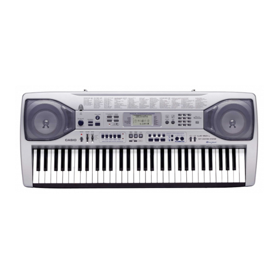
Summary of Contents for Casio LK-90TV
- Page 1 LK-90TV JUN. 2004 LK-90TV ELECTRONIC KEYBOARD INDEX Ver.1 : Jun. 2005...
-
Page 2: Table Of Contents
CONTENTS Specifications ---------------------------------------------------------------------------------------------- 1 Block Diagram --------------------------------------------------------------------------------------------- 3 Circuit Description --------------------------------------------------------------------------------------- 4 Printed Circuit Board ------------------------------------------------------------------------------------ 6 Disassembly ---------------------------------------------------------------------------------------------- 13 Diagnostic Program ------------------------------------------------------------------------------------ 19 Schematic Diagrams ----------------------------------------------------------------------------------- 22 Exploded View ------------------------------------------------------------------------------------------- 31 Parts List --------------------------------------------------------------------------------------------------- 32... -
Page 3: Specifications
32 notes maximum (16 for certain tones) Auto Accompaniment Rhythm Patterns: Tempo: Variable (226 steps, = 30 to 255) Chords: 3 fingering methods (CASIO CHORD, FINGERED, FULL RANGE CHORD) Rhythm Controller: START/STOP, INTRO, NORMAL/FILL-IN, VARIATION/FILL-IN, SYNCHRO/ENDING Accomp Volume: 0 to 127 (128 steps) <Advanced 3-Step Lesson System>... - Page 4 Terminals SUSTAIN/ASSIGNABLE JACK: Standard jack (sustain, sostenuto, soft, rhythm start/stop) HEADPHONE/OUTPUT Jack: Stereo standard jack Output Impedance: 100Ω Output Voltage: 4V (RMS) MAX Microphone In: Standard jack (with microphone volume knob) Input impedance: 3KΩ Input sensitivity: 10mV USB port VIDEO OUT Jack: Output Voltage: 1Vp-p MAX Power Jack: 9V DC...
-
Page 5: Block Diagram
BLOCK DIAGRAM — 3 —... -
Page 6: Circuit Description
CIRCUIT DESCRIPTION KEY MATRIX C2#1 D2#1 F2#1 C2#2 D2#2 F2#2 G2#1 A2#1 C3#1 D3#1 G2#2 A2#2 C3#2 D3#2 F3#1 G3#1 A3#1 F3#2 G3#2 A3#2 C4#1 D4#1 F4#1 C4#2 D4#2 F4#2 G4#1 A4#1 C5#1 D5#1 G4#2 A4#2 C5#2 D5#2 F5#1 G5#1 A5#1 F5#2 G5#2... - Page 7 KEY CONTROL/ SWO1 STEP 3 TRANSPOSE , PHRASE ALONG TRANSPOSE / MODE SWO2 STEP 1 (NOMAL) MODE TOUCH SWO3 SPEAK SCORING3 METRONOME (CASIO SCORING2 PLAY/STOP RESPONSE/ CHORD) SETTIN MODE SWO4 SPLIT RHYTHM KEY LIGHT LAYER DEMO (FINGERED) MODE TRACK1 PIANO...
-
Page 8: Printed Circuit Board
PRINTED CIRCUIT BOARDS M649-MAIN PCB Top View Bottom View — 6 —... - Page 9 M649-SUB1 PCB M649-SUB2 PCB Top View Top View Bottom View Bottom View — 7 —...
- Page 10 M649-CONSOLE PCB Top View Bottom View — 8 —...
- Page 11 M649-CONSOLE2 PCB M649-CONSOLE3 PCB M649-CONSOLE4 PCB M649-CONSOLE5 PCB M649-CONSOLE6 PCB M649-CONSOLE7 PCB Top View Top View Top View Top View Top View Top View Bottom View Bottom View Bottom View Bottom View Bottom View Bottom View M649-LCD PCB Top View Bottom View —...
- Page 12 M474-LED1 PCB Top View Bottom View M474-LED2 PCB Top View Bottom View — 10 —...
- Page 13 CSM446-LED3 PCB Top View Bottom View CSM446-LED4 PCB Top View Bottom View CSM446-LED5 PCB Top View Bottom View — 11 —...
- Page 14 M6111T-KEY1 PCB Top View Bottom View M6111T-KEY2 PCB Top View Bottom View — 12 —...
-
Page 15: Disassembly
DISASSEMBLY 1. Remove the battery cover and the batteries. 2. Remove 14 screws on the bottom of the product, and the lower plate. Note: Fix the screws in the right order when assembling. 3. Remove 19 screws on the bottom of the product. Note: Make sure to fix the screws with the arrow marks in the below figure only. - Page 16 Tip: For easier assembly, it is a good idea to give each cable a name of a corresponding connector. 6. Remove four screws and three connectors. Connector (CN13) (To M649-CNA6 PCB) Connector (CN15) (To M649-MAA3 PCB) Connector (CN17) (To M649-CNA6 PCB) 7.
- Page 17 10. Remove three screws and one connector, and then remove the M649-MAA3 PCB. 11. Remove three screws and two connectors, and then remove the M649-CNA6 PCB. M649-CNA6 PCB Connectors M649-MAA3 PCB 12. Remove two screws and the M649-CNA5 PCB. 13. Remove three screws and the M649-CNA2 PCB. M649-CNA2 PCB M649-CNA5 PCB 14.
- Page 18 18. Remove six screws and the M649-LCA1 PCB. Note: Fix the screws in the right order when assembling. 19. Remove the rubber keys. 20. Remove eight screws and two speakers. Note: Store the lead wire in the guide rail when assembling. 21.
- Page 19 22. Remove 21 screws and the keys. 23. Remove five screws and unsolder two connectors (JG, JF), and then remove the M474-LD1M PCB. 24. Remove seven screws and unsolder one connector (JE), and then remove the M474-LD2M PCB. Connector (JG) Connector (JE) (To CSM446-LD3M PCB) (To CSM446-LD5M PCB)
- Page 20 28. Remove 10 screws and the M6111T-KY1M PCB. 29. Remove nine screws and the M6111T-KY2M PCB. 30. Remove five rubber keys on the keyboard. Note: The length of this one rubber key is different. — 18 —...
-
Page 21: Diagnostic Program
DIAGNOSTIC PROGRAM Initial Setting 1. Connect the AC adaptor. 2. Connect a Sustain pedal. 3. "MODE" switch: NORMAL 4. "Main" volume: MAX 5. "MIC" volume: MIN How to start diagnostic program 1. Press the “POWER” button while pressing the “0” buttons. NOTE: Refer to the figure below for the LCD messages that appear during the diagnostic program. - Page 22 Message on LCD 2. AC adaptor check 1 Press “-” button. 3. Pedal check 1 Press “1” button. 2 “Sustain pedal”: ON 3 “Sustain pedal”: OFF 4. ROM check 1 Press “2” button. 5. MODEL check 1 Press “3” button. 6.
- Page 23 Message on LCD . KEY LED check 1 Press “SCORING1” button. * The key lights with pip sound in undermentioned the order. * There must not be remarkable difference in the LED brightness of the adjacent key. 1) C1, D1, E1, F1, G1, A1, B1 6) C1#, D1#, F1#, G1#, A1 2) C2, D2, E2, F2, G2, A2, B2 7) C2#, D2#, F2#, G2#, A2#...
-
Page 24: Schematic Diagrams
SCHEMATIC DIAGRAMS M649-MAIN PCB (1/2) — 22 —... - Page 25 M649-MAIN PCB (2/2) — 23 —...
- Page 26 M649-SUB PCB (1/2) — 24 —...
- Page 27 M649-SUB PCB (2/2) — 25 —...
- Page 28 M649-CONSOLE PCB — 26 —...
- Page 29 M649-LCD PCB — 27 —...
- Page 30 CSM446-LED PCBs — 28 —...
- Page 31 M6111T-KEY1 PCB — 29 —...
- Page 32 M6111T-KEY2 PCB — 30 —...
-
Page 33: Exploded View
EXPLODED VIEW 12 13 — 31 —... -
Page 34: Parts List
PARTS LIST LK-90TV Notes: This parts list does not include the cosmetic parts, which parts are marked with item No. "R-X" in the exploded view. Contact our spare parts department if you need these parts for refurbish. Prices and specifications are subject to change with- out prior notice. - Page 35 Price Item Parts code Parts name Specification R Remarks Code MAIN PCB 10163725 PCB ASSY/MA1 TK-RJM504075*001 A For NTSC 10163726 PCB ASSY/MA1 TK-RJM504075*002 A For PAL CN13 35022296 CONNECTOR BM04B-SRSS-TB D7-D10 23901820 DIODE 1SS355TE-17 D1-D6 79114127 DIODE RB520S-30TE61 69320063 IC R1151N001C-TR IC14 10132440 IC...
- Page 36 Price Item Parts code Parts name Specification R Remarks Code Keyboard unit 10171930 PCB ASSY/KY1M TK-RJM504262*001 10171931 PCB ASSY/KY2M TK-RJM504263*001 69273390 KEY SET/WHITE/CB M340489*003 69273400 KEY SET/WHITE/CS M340489*004 69251730 KEY SET/BLACK/5P M140369-2 69251720 KEY SET/BLACK/10P M140369-1 10012313 RUBBER/CONTACT TK-M340985*1(M454) Panel unit 10161535 REFLECTOR RJM503998-001V01 10117676 COVER SUBASSY/BATTERY TK-M340884*008...
- Page 37 Ver.1 : Jun. 2005 Correction of the EXPLODED VIEW (P31) CASIO COMPUTER CO.,LTD. Overseas Service Division 6-2, Hon-machi 1-Chome Shibuya-ku, Tokyo 151-8543, Japan...
Need help?
Do you have a question about the LK-90TV and is the answer not in the manual?
Questions and answers