Table of Contents
Advertisement
Quick Links
All manuals and user guides at all-guides.com
Service Manual
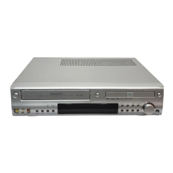
DVD COMBO RECEIVER
MODEL : DR-C912B/913B
R
L
R
L
Caution :
In this Manual, some parts can be changed for improving, their perfor-
mance without notice in the parts list. So, if you need the latest parts
information,please refer to PPL(Parts Price List) in Service Information
Center (http://svc.dwe.co.kr).
S/M No. : VCR9ADPEN0
DR-C922B/923B
VIDEO/REC
DVD/P-SCAN
VCR
DVD
REW
FF
TUNING
REC
P.SCAN
SEARCH
VCR
DVD
VCR/REC
DVD/P.SCAN
REC
P.SCAN
DAEWOO ELECTRONICS Corp.
http : //svc.dwe.co.kr
MIN
MAX
AM/FM
CH/PRESET+
SOUND FIELD
CH/PRESET—
PHONES
AM/FM
CH/PRESET+
MIN
MAX
SOUND FIELD
CH/PRESET—
PHONES
Jan., 2004
Advertisement
Table of Contents

Subscribe to Our Youtube Channel
Related Manuals for DAEWOO ELECTRONICS DR-C912B


Summary of Contents for DAEWOO ELECTRONICS DR-C912B
- Page 1 All manuals and user guides at all-guides.com S/M No. : VCR9ADPEN0 Service Manual DVD COMBO RECEIVER MODEL : DR-C912B/913B DR-C922B/923B VIDEO/REC DVD/P-SCAN AM/FM CH/PRESET+ TUNING P.SCAN SOUND FIELD CH/PRESET— SEARCH PHONES AM/FM CH/PRESET+ VCR/REC DVD/P.SCAN P.SCAN SOUND FIELD CH/PRESET— PHONES...
-
Page 2: Table Of Contents
All manuals and user guides at all-guides.com CONTENTS Page Number TROUBLESHOOTING GUIDES SPECIFICATIONS ..............1 CLEANING AND LUBRICATION...........1 POWER CIRCUIT..............72 SYSTEM CIRCUIT ..............73 TEST EQUIPMENT REQUIREMENTS ........2 THE SERVICE FIXTURE ............2 VIDEO CIRCUIT ..............78 AUDIO CIRCUIT ..............82 PATH FIXTURE CONNECTION/ TEST POINT IDENTIFICATION ........3 SCHEMATIC LEADLESS (CHIP) COMPONENT POWER SUPPLY SCHEMATIC DIAGRAM...... -
Page 3: Specifications
All manuals and user guides at all-guides.com SPECIFICATIONS Power Input :120 Volts AC 60Hz audio Input : -8.8dBm Power Consumption :95Watts Audio output (common Operating Temperature :5 degree C to 35 degree C use of DVD and VCR) : Audio output terminal (2 kinds): ( 41 degree F to 95 degree F) -8.8dBm(VCR), 2.0Vrms(DVD) Storage Temperature... -
Page 4: Test Equipment Requirements
All manuals and user guides at all-guides.com TEST EQUIPMENT REQUIREMENTS AC Millivolt Meter NTSC Video Signal Generator–Must provide 1V p-p negative Sensitivity: 1.0mVAC–400VAC sync video across a 75 ohm load and produce standard NTSC 75% saturated color bars with a 100% white window. Dual-Trace Triggered Oscilloscope–with Lo–Cap (X10) and Direct Probes. -
Page 5: Path Fixture Connection/Test Point Identification
All manuals and user guides at all-guides.com PATH FIXTURE CONNECTION/TEST POINT IDENTIFICATION Refer to the adjustment of the tape transporting system. Connect to PT01 !pin-^pin of the MAIN CIRCUIT BOARD. CTL pulse test point S/W pulse test point ENVE pulse test point LEADLESS (CHIP) COMPONENT REMOVAL INSTRUCTION •... - Page 6 All manuals and user guides at all-guides.com PATH FIXTURE CONNECTION/TEST POINT IDENTIFICATION 3. Installing the Leadless (chip) Component 4. Removing of Flat ICs(Recommended procedure) 1) Presolder the contact points of the circuit board. 1) For removing solder chips from IC's pins, use a solder remover or a wiry solder absorber.
-
Page 7: Leadless (Chip) Component Indentification
All manuals and user guides at all-guides.com LEADLESS (CHIP) COMPONENT IDENTIFICATION 1. Check the followings before S.M.D Troubleshooting • Cracked or Chipped Component Body • Rejection of Solder from Copper Pads or Component • Cracked or Separated Solder Joints • Foreign Matter on Copper Pads •... -
Page 8: Abbreviations
All manuals and user guides at all-guides.com ABBREVIATIONS A A or AUD : Audio : Drain and Source A.E. : Audio Erase DSSC : Digital Satellite Set Control : Alternating current : Decibel : Automatic Color Control : Auto Clock Set : Extended Data System : Automatic Frequency Control ENVE... - Page 9 All manuals and user guides at all-guides.com ABBREVIATIONS : Picture : Test Jump : Picture Intermediate Frequency : Test Pin : Phase Locked Loop : Transistor : Phase Shift TRANS : Transformer : Pulse Width Modulator : Tracking : Power : Tuner : Transistor U UHF...
-
Page 10: Instrument Disassembly
All manuals and user guides at all-guides.com INSTRUMENT DISASSEMBLY Perform all disassembly procedures in the order presented. When reassembling, use the reverse procedure. Make sure that all leads/wiring are routed correctly when reassembling. After Releasing two screws, Disassemble LEG Release two screws Release two screws Release three screws Fig. - Page 11 All manuals and user guides at all-guides.com INSTRUMENT DISASSEMBLY After releasing seven screws, Disassemble LOGIC PCB Fig. 4 . LOGIC PCB Removal After releasing six screws, disassemble DECK. After releasing four screws, disassemble AMP PCB. After releasing four screws, disassem- ble LOADER.
- Page 12 All manuals and user guides at all-guides.com INSTRUMENT DISASSEMBLY After Releasing one screw, Disassemble MAIN PCB Release nine screws Fig. 6. Main Board Removal After releasing six Screws, Disassemble MAIN CHASSIS Fig. 7. Chassis Main Removal...
- Page 13 All manuals and user guides at all-guides.com INSTRUMENT DISASSEMBLY...
-
Page 14: Description Of The Mechanism
All manuals and user guides at all-guides.com DESCRIPTION OF THE MECHANISM 1.1 Characteristic of T6-DECK MECHANISM 1) T6-MECHA follows the VHS and the NTSC standard. 2) T6-MECHA uses 3 MOTORS (DRUM MOTOR, CAPSTAN MOTOR, L/C MOTOR). 3) T6-MECHA uses L/C Motor to drive FRONT LOADING. 4) T6-MECHA uses 4-BIT MODE signal to recognize each MODE. - Page 15 All manuals and user guides at all-guides.com DESCRIPTION OF THE MECHANISM 1.2 WIRE DIAGRAM 1.2.1 WIRE DIAGRAM 1.2.2 CONNECTOR PIN ARRANGEMENT...
-
Page 16: Assembly Diagram And A/S
All manuals and user guides at all-guides.com ASSEMBLY DIAGRAM AND A/S 2.1. ASSEMBLY DIAGRAM 2.1.1. DECK ASSEMBLY DIAGRAM A. UPPER VIEW 1 MAINBASE ASS Y 9 IDLER PLATE TOTAL ASS Y 17 AC HEAD ASS Y 10 T BRAKE ASS Y 18 T SLANT POLE ASS Y 2 DRUM ASS Y 3 FE HEAD... - Page 17 All manuals and user guides at all-guides.com ASSEMBLY DIAGRAM AND A/S B. LOWER VIEW 1 MAINBASE ASS Y 9 IDLER PLATE TOTAL ASS Y 17 AC HEAD ASS Y 10 T BRAKE ASS Y 18 T SLANT POLE ASS Y 2 DRUM ASS Y 3 FE HEAD 11 FL RACK...
- Page 18 All manuals and user guides at all-guides.com ASSEMBLY DIAGRAM AND A/S 2.1.2. FRONT LOADING ASSEMBLY DIAGRAM Fig.2 1 FL BRKT L 2 TOP PLATE 3 SAFETY LEVER 5 CST HOLDER AS 4 LOADING LEVER AS4 6 DOOR OPENER 7 SAFETY LEVER R 8 FL BRKT R...
- Page 19 All manuals and user guides at all-guides.com ASSEMBLY DIAGRAM AND A/S 2.2 PERIODIC MAINTENANCE AND SERVICE a. Cleaning of Tape Transporting section SCHEDULE - The following parts shoule be cleaned after every 500 hours 2.2.1) Periodic maintenance and Service Schedule of use.
- Page 20 All manuals and user guides at all-guides.com ASSEMBLY DIAGRAM AND A/S 2.3 JIGS AND TOOLS 2.1 LIST OF JIGS AND TOOLS FIG. ITEMS MODEL REMARKS NTSC: SP MONOSCOPE 7KHz CHECKING OF THE ALIGNMENT TAPE SP COLOR BAR 1KHz TAPE TRANSPORTING (EP MONOSCOPE) SECTION CLEANING TAPE...
- Page 21 All manuals and user guides at all-guides.com 2..2 A SKECTCH OF JIGS AND TOOLS VHS SPINDLE HEIGHT GAUGE &...
-
Page 22: Disassembly And Replacement
All manuals and user guides at all-guides.com 3. DISASSEMBLY AND REPLACEMENT REMOVAL OF THE FRONT LOADING 3.2 DISASSEMBLY OF FRONT LOADING ASSÕY (FIG. 3.1) ASSÕY(FIG. 3.2~3.5) a. Remove the one WASHER for holding the door opener and separtate F/L Assembly by moving the DOOR OPENER in the NOTE: direction of arrow. - Page 23 All manuals and user guides at all-guides.com DISASSEMBLY AND REPLACEMENT 3. 3 Disassembly of DRUM AssÕy (Fig. 3.5) c. Separate the LOADING LEVER ASS‘Y by pressing the connection point from the CASSETTE HOLDER a. Turn over the DECK MECHANISM and holding the DRUM ASS‘Y.(Fig.
- Page 24 All manuals and user guides at all-guides.com DISASSEMBLY AND REPLACEMENT 3. 4. DISASSEMBLY OF LOADING RACK, 3. 5. DISASSEMBLY OF THE A/C HEAD LOADING ASSÕY, S/T SLANT POLE ASSÕY (FIG. 3.8) ASSÕY(FIG. 3.6, 3.7) a. Remove the CONNECTOR @ from the AC HEAD ASS‘Y, a.
- Page 25 All manuals and user guides at all-guides.com DISASSEMBLY AND REPLACEMENT 3. 6. DISASSEMBLY OF THE LC BRKT ASSÕY, PINCH LEVER TOTAL ASSÕY (FIG. 3.9) a. Separate the LC BRKT Ass y @ after removing the 3 screws b. Separate the LC BRKT Ass y @ from the DECK MECHANISM. c.
- Page 26 All manuals and user guides at all-guides.com DISASSEMBLY AND REPLACEMENT 3. 8 DISASSEMBLY OF THE S/T BRAKE 3.11 DISASSEMBLY OF THE FE HEAD (FIG. ASSÕY(FIG. 3.12) 3.13) a. Unhook the S BRAKE SPRING # from the MAINBASE HOOK a. Remove the screw ^ and separate the FE HEAD & from the MAINBASE.
- Page 27 All manuals and user guides at all-guides.com DISASSEMBLY AND REPLACEMENT 3.12 DISASSEMBLY OF THE REEL TABLE, 3.13 DISASSEMBLY OF THE REEL BRKT IDLER PLATE TOTAL ASSÕY (FIG. 3.15) TOTAL ASSÕY, CONNECT PLATE (FIG. 3.16) a. Remove the POLY WASHER ! and separate the IDLER PLATE TOTAL Ass y @ from the mainbase.
-
Page 28: Mechanical Adjustment
All manuals and user guides at all-guides.com MECHANICAL ADJUSTMENT 4. 1 MECHANICAL ADJUSTMENT (FIG. 4.1~4.4) In case of diassembly and reassembly for fixng the mecanical prob- lem, check the following check point. a. Make sure that the DATUM HOLE of the CAM GEAR is aligned wth the DATUM HOLE in the MAINBASE in the EJECT modew as shown in Fig. - Page 29 All manuals and user guides at all-guides.com MECHANICAL ADJUSTMENT 4. 2 ADJUSTMENT AND MEASUREMENT OF d. Make sure that the triangular mark A of the L LOADING Ass y is aligned with the mark b of the R LOADING Ass y. (Fig. 4.4) THE BACK TENSION (FIG.
- Page 30 All manuals and user guides at all-guides.com MECHANICAL ADJUSTMENT 4. 3 MECHANICAL MODE (OPERATE WITH- OUT A CASSETTE TAPE) a. Remove the FRONT LOADING MECHANISM from the DECK MECHANISM b. Cap the IR LED and pull the FL RACK. This has the same effect with cassette loading to the deck.
-
Page 31: Adjustment Of The Tape Transport Section
All manuals and user guides at all-guides.com ADJUSTMENT OF THE TAPE TRANSPORT SECTION. Generally, tape transporting section has been precisely adjusted in the factory and does not require the ordinary readjustment. But there is the case that tape noise or impact on the deck mechanism, tape transporting section readjustment is required. In adjustment of the tape transmission section consut the following flow chart. - Page 32 All manuals and user guides at all-guides.com ADJUSTMENT OF THE TAPE TRANSPORT SECTION CLEANING S/T GUIDE ROLLER HEIGHT • DRUM TOTAL AS ADJUSTMENT S/T GUIDE ROLLER FLUNGE • A/C HEAD AS • PINCH LEVER TOTAL A/C HEAD AS ADJUSTMENT (TILT ADJUSTMENT) AUDIO AZIMUTH ADJUSTMENT A/C HEAD ADJUSTMENT X-POSITION ADJUSTMENT...
- Page 33 All manuals and user guides at all-guides.com ADJUSTMENT OF THE TAPE TRANSPORT SECTION A. ADJUSTMENT OF THE S/T GUIDE D. ADJUSTMENT OF THE AUDIO ROLLER AZIMUTH(FIG. 5.4) A. Adjustment of the S/T GUIDE ROLLER a. Play back the ALIGNMENT TAPE a.
- Page 34 All manuals and user guides at all-guides.com ADJUSTMENT OF THE TAPE TRANSPORT SECTION G. ADJUSTMENT OF THE LINEARITY(FIG. 5.7) S/W PULSE TEST PIN PATH ADJ. FIXTURE Test Point ENVELOPE TEST PIN PATH ADJ.FIXTURE Measurement Equipment OSILLOSCOPE VR CONTROL PATH ADJ.FIXTURE Adjustment S/T GUIDE ROLLER TAPE TRANSPORT SECTION...
- Page 35 All manuals and user guides at all-guides.com ADJUSTMENT OF THE TAPE TRANSPORT SECTION H. ADJUSTMENT OF THE WAVE FORM OF e. Make the VR CONTROL on the PATH ADJ. FIXTURE to the DRUM ENTRANCE /EXIT (FIG. 5.8) center to maximize the ENVELOPE signal. f.
- Page 36 All manuals and user guides at all-guides.com ADJUSTMENT OF THE TAPE TRANSPORT SECTION K. ADJUSTMENT OF THE AUDIO AZIMUTH L. X-POSITION S/W PULSE TEST PIN PATH ADJ. FIXTURE Test Point Test Point AUDIO OUTPUT AUDIO OUTPUT JACK ENVELOPE TEST PIN PATH ADJ.FIXTURE Measurement Equipment AUDIO LEVEL METER...
-
Page 37: Exploded View
All manuals and user guides at all-guides.com EXPLODED VIEW 6.1 EXPLODED VIEW OF DECK ASSÕY ( TOP VIEW) - Page 38 All manuals and user guides at all-guides.com EXPLODED VIEW 6. 2 EXPLODED VIEW OF DECK ASSÕY ( BOTTOM VIEW)
- Page 39 All manuals and user guides at all-guides.com EXPLODED VIEW 6.3 EXPLODED VIEW OF FL ASSÕY...
- Page 40 All manuals and user guides at all-guides.com EXPLODED VIEW D0040 D0020 D0040 D0050 D0010 D0060 D0070...
- Page 41 All manuals and user guides at all-guides.com EXPLODED VIEW PART NAME PART NO. Q’TY MATERIAL REMARK...
-
Page 42: Electrical Adjustment
All manuals and user guides at all-guides.com ELECTRICAL ADJUSTMENT Fig. 1 Main board test point/control location guide(component) - Page 43 All manuals and user guides at all-guides.com ELECTRICAL ADJUSTMENT PG (Pulse Generator) Shifter Adjustment (Fig. 3) PT01 PIN # Test Points: Main Video Out Jack Rear Panel Adjust: REC SWITCH Main The Pulse Generator (PG) Shifter determines the video head switching point during playback.
-
Page 44: Waveforms
All manuals and user guides at all-guides.com WAVEFORMS VIDEO WAVEFORMS... - Page 45 All manuals and user guides at all-guides.com WAVEFORMS AUDIO WAVEFORMS AUDIO(Normal) (IC301-76) 150mVp-p (IC301-10) 1.5Vp-p (IC301-9) 2.3Vp-p (IC301-2) 120mVp-p 20mV/0.5msec/cm 0.5V/0.5msec/cm 0.5V/0.5msec/cm 50mV/0.5msec/cm PLAY (P201-2) 75Vp-p 10V/20µsec/cm AUDIO(Hi-Fi) (IC251-10) 80mVp-p (IC251-19) 200mVp-p (IC251-21) 1.8Vp-p (IC251-29) 1.2Vp-p 20mV/0.5msec 50mV/0.5msec 0.5V/1msec 0.2V/2msec EE/REC/PLAY EE/REC PLAY...
- Page 46 All manuals and user guides at all-guides.com WAVEFORMS SERVO WAVEFORMS...
- Page 47 All manuals and user guides at all-guides.com WAVEFORMS AMP AUDIO WAVEFORMS BCK DDX-8000(IC200) PIN#11 Amp Micom(IC220) Amp Micom(IC220) MCLK DDX-8000 (IC200) PIN#20(AMP CLK) PIN#21(AMP CLK) PIN#20 LRCK DDX-8000 (IC200) PCM1(Front L/R) DDX-8000 PCM2(CEN/SUB) DDX-8000 PCM0(downmix) DDX-8000 PIN#10 (IC200) PIN#9 (IC200) PIN#7 (IC200) PIN#6 PCM3(Rear L/R) AMP Micom (IC220)
-
Page 48: Voltage Charts
All manuals and user guides at all-guides.com VOLTAGE CHART 1. SERVO/SYSCON/TIMER MI-COM MODE IC MI-COM (IC601) MODE IC MI-COM (IC601) REW/ REV/FWD PLAY REW/ REV/FWD PLAY PIN No. PIN No. STOP PLAY STOP PLAY F.FWD SEARCH PAUSE PAUSE F.FWD SEARCH PAUSE PAUSE vary... -
Page 49: Ic Eeprom/Sync Srpa/Reset/Tr
All manuals and user guides at all-guides.com VOLTAGE CHART MODE IC MI-COM (IC601) REW/ REV/FWD PLAY PIN No. STOP PLAY F.FWD SEARCH PAUSE PAUSE 2. IC EEPROM/SYNC SRPA/RESET/TR VOLTAGE CHARTS MODE IC EEPROM(IC603) MODE IC EEPROM(IC603) REW/ REV/FWD PLAY REW/ REV/FWD PLAY PIN No. -
Page 50: Ic Driver/Switch
All manuals and user guides at all-guides.com VOLTAGE CHART 3. IC DRIVER/SWITCH VOLTAGE CHARTS MODE IC DRIVER (IC701) MODE IC DRIVER (IC701) REW/ REV/FWD PLAY REW/ REV/FWD PLAY PIN No. PIN No. STOP PLAY STOP PLAY F.FWD SEARCH PAUSE PAUSE F.FWD SEARCH PAUSE... -
Page 51: Video(Luma/Chroma) And Linear Audio
All manuals and user guides at all-guides.com VOLTAGE CHART 4. VIDEO(LUMA/CHROMA) AND LINEAR AUDIO VOLTAGE CHARTS MODE IC VIDEO/AUDIO (IC301) MODE IC VIDEO/AUDIO (IC301) REW/ REV/FWD PLAY REW/ REV/FWD PLAY PIN No. PIN No. STOP PLAY STOP PLAY F.FWD SEARCH PAUSE PAUSE F.FWD... -
Page 52: Video Switching Ic Voltage Charts
All manuals and user guides at all-guides.com VOLTAGE CHART 5. VIDEO SWITCHING IC VOLTAGE CHARTS MODE IC401 MODE IC DRIVER (IC701) REW/ REV/FWD PLAY REW/ REV/FWD PLAY PIN No. PIN No. STOP PLAY STOP PLAY F.FWD SEARCH PAUSE PAUSE F.FWD SEARCH PAUSE PAUSE... -
Page 53: Hifi Audio Ic
All manuals and user guides at all-guides.com VOLTAGE CHART 6. HIFI AUDIO IC VOLTAGE CHARTS MODE IC Hi-Fi (IC251) MODE IC VIDEO/AUDIO (IC301) REW/ REV/FWD PLAY REW/ REV/FWD PLAY PIN No. PIN No. STOP PLAY STOP PLAY F.FWD SEARCH PAUSE PAUSE F.FWD SEARCH... -
Page 54: Tmi
All manuals and user guides at all-guides.com VOLTAGE CHART 8. TMI VOLTAGE CHART MODE TMI (RF101) MODE TMI (RF101) REW/ REV/FWD PLAY REW/ REV/FWD PLAY PIN No. PIN No. STOP PLAY STOP PLAY F.FWD SEARCH PAUSE PAUSE F.FWD SEARCH PAUSE PAUSE 31.4 31.4... -
Page 55: Amp Mi-Com
All manuals and user guides at all-guides.com VOLTAGE CHART 10. AMP MI-COM VOLTAGE CHART(W78E58BP-42) 1. DVD MODE 2. EXTERNAL INPUT 1) VCR MODE... - Page 56 All manuals and user guides at all-guides.com VOLTAGE CHART 2) AM/FM MODE *1 : It is changed according to the state of AM/FM. *2 : It is changed according to the option resistances(R205, R206, R207, R208, R209). - Existing option resistances : 0V - No existing option resistances : 5.2V...
-
Page 57: Amp Ddx-8000
All manuals and user guides at all-guides.com VOLTAGE CHART 11. AMP DDX-8000 VOLTAGE CHART(DDX-8000) 1. SPEAKER SETUP : Default, Configuration1 1) DVD IC DDX-8000(IC200) IC DDX-8000(IC200) MODE MODE 5.1CH 5.1CH PLAY PLAY PLAY PLAY STOP PLAY MUTE STOP PLAY MUTE STOP PLAY MUTE STOP PLAY MUTE... - Page 58 All manuals and user guides at all-guides.com VOLTAGE CHART 1) EXTERNAL INPUT (1) VIDEO MODE IC DDX-8000(IC200) IC DDX-8000(IC200) MODE MODE 5.1CH 5.1CH PLAY PLAY PLAY PLAY STOP PLAY MUTE STOP PLAY MUTE STOP PLAY MUTE STOP PLAY MUTE PINNO. PINNO.
- Page 59 All manuals and user guides at all-guides.com VOLTAGE CHART (2) AM/FM MODE IC DDX-8000(IC200) IC DDX-8000(IC200) MODE MODE 5.1CH 5.1CH PINNO. PINNO. 3.35 3.35 3.35 3.35 3.35 3.35 3.35 3.35...
- Page 60 All manuals and user guides at all-guides.com VOLTAGE CHART 2. SPEAKER SETUP : Configuration 2 , 3 1) DVD IC DDX-8000(IC200) IC DDX-8000(IC200) MODE MODE 5.1CH 5.1CH PLAY PLAY PLAY PLAY STOP PLAY MUTE STOP PLAY MUTE STOP PLAY MUTE STOP PLAY MUTE PINNO.
- Page 61 All manuals and user guides at all-guides.com VOLTAGE CHART 2) EXTERNAL INPUT (1) VIDEO MODE IC DDX-8000(IC200) IC DDX-8000(IC200) MODE MODE 5.1CH 5.1CH PLAY PLAY PLAY PLAY STOP PLAY MUTE STOP PLAY MUTE STOP PLAY MUTE STOP PLAY MUTE PINNO. PINNO.
- Page 62 All manuals and user guides at all-guides.com VOLTAGE CHART (2) AM/FM MODE IC DDX-8000(IC200) IC DDX-8000(IC200) MODE MODE 5.1CH 5.1CH PINNO. PINNO. 3.35 3.35 3.35 3.35 3.35 3.35 3.35 3.35...
-
Page 63: Amp Ddx-2100
All manuals and user guides at all-guides.com VOLTAGE CHART 12. AMP DDX-2100 VOLTAGE CHART(DDX-2100) 1. SPEAKER SETUP : Default , configuration1 1) DVD DDX-2100(IC301) DDX-2100(IC301) MODE MODE 5.1CH 5.1CH PLAY PLAY PLAY PLAY STOP PLAY MUTE STOP PLAY MUTE STOP PLAY MUTE STOP PLAY... - Page 64 All manuals and user guides at all-guides.com VOLTAGE CHART DDX-2100(IC360) DDX-2100(IC360) MODE MODE 5.1CH 5.1CH PLAY PLAY PLAY PLAY STOP PLAY MUTE STOP PLAY MUTE STOP PLAY MUTE STOP PLAY MUTE PINNO. PINNO. PAUSE PAUSE PAUSE PAUSE 32.5 32.5 32.5 32.5 32.5 32.5...
- Page 65 All manuals and user guides at all-guides.com VOLTAGE CHART DDX-2100(IC330) DDX-2100(IC330) MODE MODE 5.1CH 5.1CH PLAY PLAY PLAY PLAY STOP PLAY MUTE STOP PLAY MUTE STOP PLAY MUTE STOP PLAY MUTE PINNO. PINNO. PAUSE PAUSE PAUSE PAUSE 32.5 32.5 32.5 32.5 32.5 32.5...
- Page 66 All manuals and user guides at all-guides.com VOLTAGE CHART (2) AM/FM MODE MODE IC DDX-2100(IC301) MODE IC DDX-2100(IC301) 5.1CH 5.1CH PINNO. PINNO. 32.5 32.5 32.5 32.5 32.5 32.5 32.5 32.5 32.5 32.5 32.5 32.5 32.5 32.5 32.5 32.5 32.5 32.5 32.5 32.5 32.5...
- Page 67 All manuals and user guides at all-guides.com VOLTAGE CHART MODE IC DDX-2100(IC360) MODE IC DDX-2100(IC360) 5.1CH 5.1CH PINNO. PINNO. 32.5 32.5 32.5 32.5 32.5 32.5 32.5 32.5 32.5 32.5 32.5 32.5 32.5 32.5 32.5 32.5 32.5 32.5 32.5 32.5 32.5 32.5 32.5 32.5...
- Page 68 All manuals and user guides at all-guides.com VOLTAGE CHART DDX-2100(IC330) DDX-2100(IC330) MODE MODE 5.1CH 5.1CH PLAY PLAY PLAY PLAY STOP PLAY MUTE STOP PLAY MUTE STOP PLAY MUTE STOP PLAY MUTE PINNO. PINNO. PAUSE PAUSE PAUSE PAUSE 32.5 32.5 32.5 32.5 32.5 32.5...
- Page 69 All manuals and user guides at all-guides.com VOLTAGE CHART 2) EXTERNAL INPUT (1) VIDEO MODE DDX-2100(IC301) DDX-2100(IC301) MODE MODE 5.1CH 5.1CH PLAY PLAY PLAY PLAY STOP PLAY MUTE STOP PLAY MUTE STOP PLAY MUTE STOP PLAY MUTE PINNO. PINNO. PAUSE PAUSE PAUSE PAUSE...
- Page 70 All manuals and user guides at all-guides.com VOLTAGE CHART DDX-2100(IC360) DDX-2100(IC360) MODE MODE 5.1CH 5.1CH PLAY PLAY PLAY PLAY STOP PLAY MUTE STOP PLAY MUTE STOP PLAY MUTE STOP PLAY MUTE PINNO. PINNO. PAUSE PAUSE PAUSE PAUSE 32.5 32.5 32.5 32.5 32.5 32.5...
- Page 71 All manuals and user guides at all-guides.com VOLTAGE CHART MODE ICDDX-2100(IC330) MODE IC DDX-2100(IC330) 5.1CH 5.1CH PIN NO. PINNO. 32.5 32.5 32.5 32.5 32.5 32.5 32.5 32.5 32.5 32.5 32.5 32.5 32.5 32.5 32.5 32.5 32.5 32.5 32.5 32.5 32.5 32.5 32.5 32.5...
-
Page 72: Ic Smps/Fet/Photo Coupler/Regulator/Tr
All manuals and user guides at all-guides.com VOLTAGE CHART IC SMPS/FET/PHOTO COUPLER/REGULATOR/TR VOLTAGE CHARTS MODE SMPS Controller(IC801) [V] MODE SMPS Controller(IC801) [V] PIN No. PIN No. PWR ON DVD PLAY DVDOFF DVD PLAY FM/AM PWR ON DVD PLAY DVDOFF DVD PLAY FM/AM &... - Page 73 All manuals and user guides at all-guides.com VOLTAGE CHART MODE IC REGULATOR(IC902) [V] MODE FET(Q903)[V] PIN No. PIN No. PWR ON DVD PLAY DVDOFF DVD PLAY FM/AM PWR ON DVD PLAY DVDOFF DVD PLAY FM/AM & VCR OFF VCR PLAY &VCR REC &...
-
Page 74: Power Circuit
All manuals and user guides at all-guides.com TROUBLESHOOTING POWER CIRCUIT Caution: When checking the primary circuit, be sure to use an isolation transformer. No power Exchange POWER CORD POWER cord is ok? Check D801, TH801, Is 120~200V voltage obtained at C801+? F801,LX801, LX802. -
Page 75: System Circuit
All manuals and user guides at all-guides.com TROUBLESHOOTING SYSTEM CIRCUIT A. VFD DISPLAY No VFD display. Is 5V obtained at IC701 pin#13? Check D721. Is -24V obtained at IC701 Check POWER circuit at -24V. pin#30? Oscillation at IC701 pin #8? Check IC701. - Page 76 All manuals and user guides at all-guides.com TROUBLESHOOTING B. No power compensation. No power compensation. Voltage of power fail (IC601 Check R625. pin#100) at micom is 0.7V over? More than 3.2V is maintained for 1 minutes at IC601 pin#37 Check RESET circuit. during Power Cord Open.
- Page 77 All manuals and user guides at all-guides.com TROUBLESHOOTING C-2. Bad playback quality (2) Noise appears on the Full Recheck step C-1 (Bad playback screen. playback quallty (1)). Are SW pulse and HA SW Are there SW, HA SW pulse at Check IC601.
- Page 78 All manuals and user guides at all-guides.com TROUBLESHOOTING E. No CASSETTE Loading Cassette tape isn’t inserted. Is 5V voltage obtained at Check at Power Circuit 14V. Loading parts IC601 pin#82? Check (D905, D906). Is 13V voltage obtained at Check D851 (Main circuit). Capstan Motor pin#8? Connect Capstan and Loading Motor.
- Page 79 All manuals and user guides at all-guides.com TROUBLESHOOTING G. DRUM Motor stops DRUM Motor stops. Is 13V voltage obtained at Check 14V P603 pin#8? (P601 #9). Is DRUM PWM fit to IC 601 Check DRUM PG/FG(IC 601 90). pin#76? Is 1.2V voltage obtained at Check R657, R658,C661,C668.
-
Page 80: Video Circuit
All manuals and user guides at all-guides.com TROUBLESHOOTING VIDEO CIRCUIT A. EE screen doesn’t appear EE screen doesn’t appear. Is video signal input at Check IC401, LINE JACK and IC301 pin#28, 30, 32? IF circuit. Is 5V obtained at IC301 Check power circiut. - Page 81 All manuals and user guides at all-guides.com TROUBLESHOOTING B. Playback picture doesn’t appear Playback picture doesn’t appear. Is C.S, DATA, CLOCK signal Check IC pin#61, 71, 72. input IC301 pin#53,54,55? Is envelope output at IC301 Is 5V obtained at IC301 pin#68? Check power circuit.
- Page 82 All manuals and user guides at all-guides.com TROUBLESHOOTING C. No recording No recording. Check EE MODE. Is FM signal output at IC301 Is signal input at IC301 pin# pin#14? 28, 30,32? Is 5V obtained at IC301 Check POWER circuit. pin#68? Is VIDEO SW Pulse input at Check IC601 pin#18.
- Page 83 All manuals and user guides at all-guides.com TROUBLESHOOTING E. No Logo Display or Do not open tray.(DVD) No Logo display. Do not open tray Is video mode-S-Video Change video mode. mode? Is power_on_H signal output at Is power supplied CN2? Check POWER circuit.
-
Page 84: Audio Circuit
All manuals and user guides at all-guides.com TROUBLESHOOTING AUDIO CIRCUIT 1. RCA A. No sound in E-E mode A-1. TV E-E No sound in RF E-E mode Is 12V obtained at IC251 pin#58? Check POWER circuit. Is 5V obtained at IC251 pin#40? Is there SIF signal at IC251 Check RF101. - Page 85 All manuals and user guides at all-guides.com TROUBLESHOOTING A-2. LINE1 E-E No sound in LINE1 E-E mode. Is 12V obtained at IC251 pin#58? Check POWER circuit. Is 5V obtained at IC251 pin#40? Replace IC 252 IC 12V Is there at Is there H at Check Input LINE1 Is Audio signal at IC251...
- Page 86 All manuals and user guides at all-guides.com TROUBLESHOOTING A-3. LINE2 E-E No sound in LINE2 E-E mode. Is 12V obtained at IC251 pin#58? Check POWER circuit. Is 5V obtained at IC251 pin#40? Replace IC 252 IC 12V Is there H at Is there at Check Input LINE2 Is Audio signal at IC251...
- Page 87 All manuals and user guides at all-guides.com TROUBLESHOOTING A-4. LINE3 (FRONT) E-E No sound in LINE3(FRONT) E-E mode. Is 12V obtained at IC251 pin#58? Check POWER circuit. Is 5V obtained at IC251 pin#40? Replace IC 252 IC 12V Is there H at Is there at Check Input LINE3 Is Audio signal at IC251...
- Page 88 All manuals and user guides at all-guides.com TROUBLESHOOTING A-5. DVD E-E NO sound DVD EE mode. Are there voltage at ICD01 Check POWER circuit. #8(5V), #9(3.3V), #21(5V)? Are there clocks at ICD01 #5(BCLK), Check DVD Board. #6(LRCLK), #10(MCLK)? Check signal flow circuit. Is there reset at ICD01 #14? Is 12V obtained at ICD02 #8? Check ICD02...
- Page 89 All manuals and user guides at all-guides.com TROUBLESHOOTING A-6. SUBWOOFER PRE-OUT E-E NO sound Subwoofer pre- out EE mode. Is Speaker setup default or Subwoofer output is only in the configuration1? default or configuration1. Are there voltages at ICD01 #8(5V), Check Power circuit.
- Page 90 All manuals and user guides at all-guides.com TROUBLESHOOTING B. No Hi-Fi playback audio (PLAY MODE) Is 12V obtained at IC251 pin#58? Check POWER circuit. Is 5V obtained at IC251 pin#40? Is there Hi-Fi(H) at IC251 Check DRUM connector and pin#28? DRUM.
- Page 91 All manuals and user guides at all-guides.com TROUBLESHOOTING c. No Hi-Fi playback in record/playback mode(REC MODE) Check input LINE1 JACK. Are there Audio signal Check input LINE2 JACK. at IC251 pin#9,14 Check input LINE3(Front) #10, 15 JACK. #2,4? Is there REC(H) Check IC601 pin#22 at IC251 pin#29, 30? Is FM OSC signal at IC251...
- Page 92 All manuals and user guides at all-guides.com TROUBLESHOOTING D. No NORMAL AUDIO playback (PLAY MODE) Voltage at IC251 pin#58 is Is there normal Audio signal 12V? Voltage at IC251 pin#40 Check power circuit. at IC251 pin#53, 57? and at IC301 pin#77 is 5V? Is Playback Audio signal at Check A/C HEAD and IC301 IC301 pin#10?
- Page 93 All manuals and user guides at all-guides.com TROUBLESHOOTING E. No NORMAL AUDIO playback in record/playback mode(Check in REC mode) No Normal Audio playback in record/playback mode Check Input LINE1 JACK. Are there Audio signal at Check Input LINE2 JACK. IC251 pin#9,14 Check input LINE3(Front) #10,15 #2,4?
- Page 94 All manuals and user guides at all-guides.com TROUBLESHOOTING 2. HEADPHONE NO sound in DVD or EXTERNAL mode. Are there voltages at ICD01 #8(5V), Check Power circuit. #9(3.3V), #21(5V)? Are there clocks at ICD01 #5(BCLK), Check DVD Board. #6(LRCLK), #10(MCLK)? Check signal flow circuit. Is there reset(H) at ICD01 #14? Is 12V obtained at ICD03 #8? Are there signals at ICD04...
- Page 95 All manuals and user guides at all-guides.com TROUBLESHOOTING No sound in the DVD MODE. Is+3.3V obtained at IC200 Check power circuit. VDD_3.3? Is+2.5V obtained at IC200 VDD_2.5? Is+3.3V obtained at the IBIAS of IC301,IC330,IC360? Is+32.5V obtained at the Vcc of IC301,IC330,IC360? Is there ‘H’...
- Page 96 All manuals and user guides at all-guides.com TROUBLESHOOTING The volume is not operating Is+5V obtained at IC220 #9, Check power circuit. #35, #44? Is+3.3V obtained at IC200 VDD_3.3? Is+2.5V obtained at the IC220 VDD_2.5? Check IC601 and Data Is there ‘L’ at IC220 #10? ports.
- Page 97 All manuals and user guides at all-guides.com TROUBLESHOOTING The protect takes place in the Are the #4,#7,#12,#17 of IC Check IC301, IC330,IC360 and 301, IC330,IC360 connected to replace inferior device the ground? Are the #2~3, #8~9,#10~11,#16~17 of Check Power circuit IC301,IC330,IC360 connected the ground? Is+4V obtained at...
- Page 98 All manuals and user guides at all-guides.com TROUBLESHOOTING No sound in the Radio MODE. Is +12V obtained at RF102 #3? Check power circuit. Check IC220 and When tunning play are there communication withe IC601. normal PLL control signals at IC220 #3~#6? When tuned, is there ‘L’...
- Page 99 All manuals and user guides at all-guides.com TROUBLESHOOTING No sound in External(Video) MODE. Are there Voltage at ICD01 Check power circuit. #18(5V) #9(3.3V), #21(5V)? Are there normal audio signals Check signal flow circuit. at ICD01 #16~#17, #19~20? Are there clock at Check DVD Board.
-
Page 100: Power Supply Schematic Diagram
All manuals and user guides at all-guides.com SCHEMATIC DIAGRAM POWER SUPPLY SCHEMATIC DIAGRAM R714 C707 4.7 5W(OPEN) 102 1KV(OPEN) T701 B702 DV8T911N3A D704 L701 3557 (EER-42/4215(V)) SF3006PT DR22(22uH) 32V/7A R701 R702 68K 2W C701 R715 47K 1W 103 1KV BH144-55 C709 C710 2.7K 2W... -
Page 101: Servo & Syscon Schematic Diagram (Dvd Combo Receiver)
All manuals and user guides at all-guides.com SCHEMATIC DIAGRAM SERVO & SYSCON SCHEMATIC DIAGRAM (DVD COMBO RECEIVER) -
Page 102: Video/Audio Schematic Diagram (Dvd Combo Receiver)
All manuals and user guides at all-guides.com SCHEMATIC DIAGRAM VIDEO/AUDIO SCHEMATIC DIAGRAM (DVD COMBO RECEIVER) -
Page 103: Hi-Fi & S/W & Pif & Mpx Schematic Diagram (Dvd Combo Receiver)
All manuals and user guides at all-guides.com SCHEMATIC DIAGRAM Hi-Fi & S/W & PIF & MPX SCHEMATIC DIAGRAM (DVD COMBO RECEIVER) -
Page 104: Digital Audio/Video Schematic Diagram(Dvd Combo Receiver)
All manuals and user guides at all-guides.com SCHEMATIC DIAGRAM DIGITAL AUDIO/VIDEO SCHEMATIC DIAGRAM(DVD COMBO RECEIVER) -
Page 105: Receiver Front Part Schematic Diagram
All manuals and user guides at all-guides.com SCHEMATIC DIAGRAM RECEIVER FRONT PART SCHEMATIC DIAGRAM... -
Page 106: Digital Amp Schematic Diagram
All manuals and user guides at all-guides.com SCHEMATIC DIAGRAM DIGITAL AMP SCHEMATIC DIAGRAM... -
Page 107: Dvd Schematic Diagram
All manuals and user guides at all-guides.com SCHEMATIC DIAGRAM DVD SCHEMATIC DIAGRAM 1. ATAPI I/F HDD[0..15] HDD0 HDD1 HDD2 HDD3 HDD4 HDD5 HDD6 HDD7 HDD8 HDD9 HDD10 HDD11 HDD12 HDD13 HDD14 HDD15... - Page 108 All manuals and user guides at all-guides.com SCHEMATIC DIAGRAM DVD SCHEMATIC DIAGRAM 2. DVD PROCESSOR DQM[0:3] DIG_3V3 DAC_3V3 R133 WE L WE L R134 RASL RASL CASL R135 CASL MCKEN R136 MCKEN R137 100R MCKO MCKO TC44 TC45 DR_MAP 47uF/6V DR_MAP DR_BS0 47uF/6V...
- Page 109 All manuals and user guides at all-guides.com SCHEMATIC DIAGRAM DVD SCHEMATIC DIAGRAM 3. Memory Interface MA[0..11] MA[0..11] MA[0..11] MA[0:11] MD[0..31] MD[0..31] MD[0:31] N_CSL N_CSL N_CSL N_OEL N_OEL N_OEL N_OEL N_WEL N_WEL N_WEL N_WEL DIG_3V3 TC59S6432CFT-80 DIG_3V3 ROMULATOR-60 C112 CONNECTOR MD31 C111 0.1uF 0.1uF DQ31...
- Page 110 All manuals and user guides at all-guides.com SCHEMATIC DIAGRAM DVD SCHEMATIC DIAGRAM 4. POWER & Bypass Cap DIG_3V3 DIG_1V8 HEAT SINK AREA FOR LT1117CST-ADJ U1 : FOR THE DEVICE, ALLOW 25MM SQ VOUT COPPER AREA ON LAYER 1. THAT IS CONNECTED TO THE "TAB"...
- Page 111 All manuals and user guides at all-guides.com SCHEMATIC DIAGRAM DVD SCHEMATIC DIAGRAM 5. VIDEO & AUDIO...
-
Page 112: Block Diagram
All manuals and user guides at all-guides.com BLOCK DIAGRAM RECEIVER SERVO & SYSCON BLOCK DIAGRAM... -
Page 113: Combo Receiver Video Block Diagram
All manuals and user guides at all-guides.com BLOCK DIAGRAM COMBO RECEIVER VIDEO BLOCK DIAGRAM... -
Page 114: Normal Audio Block Diagram
All manuals and user guides at all-guides.com BLOCK DIAGRAM NORMAL AUDIO BLOCK DIAGRAM... -
Page 115: Hi-Fi &Sw & Pif Block Diagram
All manuals and user guides at all-guides.com BLOCK DIAGRAM Hi-Fi & S/W & PIF BLOCK DIAGRAM DRC6000N, DRC6000L Hi-Fi AUDIO BLOCK DIAGRAM REV.0 2002.09.03... -
Page 116: Digital Audio Block Diagram
All manuals and user guides at all-guides.com BLOCK DIAGRAM DIGITAL AUDIO BLOCK DIAGRAM... -
Page 117: Amp Block Diagram
All manuals and user guides at all-guides.com BLOCK DIAGRAM AMP BLOCK DIAGRAM... -
Page 118: Circuit Board Index
All manuals and user guides at all-guides.com CIRCUIT BOARD INDEX MAIN PCB CIRCUIT BOARD(RTD300) -
Page 119: Power/Logic Pcb
All manuals and user guides at all-guides.com CIRCUIT BOARD INDEX POWER/LOGIC PCB CIRCUIT BOARD(RTD300) -
Page 120: Amp Pcb
All manuals and user guides at all-guides.com CIRCUIT BOARD INDEX AMP PCB CIRCUIT BOARD(RTD300) -
Page 121: Electrical Partlist
All manuals and user guides at all-guides.com ELECTRICAL PARTSLIST Caution: In this Service Manual, some parts can be changed for improving, their performance without notice in the parts list. So, if you need the latest parts information, please refer to PPL(Parts Price List) in Service information Center(http://svc.dwe.co.kr) PARTS_CODE PARTS_NAME PARTS_DESCRIPTION... - Page 122 All manuals and user guides at all-guides.com ELECTRICAL PARTSLIST PARTS_CODE PARTS_NAME PARTS_DESCRIPTION REMARK PARTS_CODE PARTS_NAME PARTS_DESCRIPTION REMARK C311 HCBK104KBA C CHIP CERA 50V X7R 0.1MF K 1608 Main PCB C628 HCQK130JBA C CHIP CERA 50V CH 13PF J 1608 Main PCB C312 CEXF1C100A C ELECTRO...
- Page 123 All manuals and user guides at all-guides.com ELECTRICAL PARTSLIST PARTS_CODE PARTS_NAME PARTS_DESCRIPTION REMARK PARTS_CODE PARTS_NAME PARTS_DESCRIPTION REMARK CD30 CEXF1C100A C ELECTRO 16V RSM 10MF 5X7 Main PCB D108A DZUZ7R5BSC DIODE ZENER UZ-7.5BSC(7.33-7.64) Main PCB CD33 CEXF1C220A C ELECTRO 16V RSM 22MF (5X7) Main PCB D109 DZUZ5R1BSB...
- Page 124 All manuals and user guides at all-guides.com ELECTRICAL PARTSLIST PARTS_CODE PARTS_NAME PARTS_DESCRIPTION REMARK PARTS_CODE PARTS_NAME PARTS_DESCRIPTION REMARK L103 5CPX688K2T COIL PEAKING 0.68UH(BLU-SILV) Main PCB Q201 TZTA1266Y- KTA1266Y- (AUTO)(1015Y) Main PCB L104 5CPX101J2T COIL PEAKING 100UH(BRN-BRN) Main PCB Q202 TZTC3202Y- KTC3202Y (AUTO)(1959Y) Main PCB L105 5CPX101J2T...
- Page 125 All manuals and user guides at all-guides.com ELECTRICAL PARTSLIST PARTS_CODE PARTS_NAME PARTS_DESCRIPTION REMARK PARTS_CODE PARTS_NAME PARTS_DESCRIPTION REMARK R205 HRFS273JBA R CHIP 1/16 27K OHM J 1608 Main PCB R288 RD-AZ471J- R CARBON FILM 1/6 470 OHM J Main PCB R206 HRFS821JBA R CHIP 1/16 820 OHM J 1608...
- Page 126 All manuals and user guides at all-guides.com ELECTRICAL PARTSLIST PARTS_CODE PARTS_NAME PARTS_DESCRIPTION REMARK PARTS_CODE PARTS_NAME PARTS_DESCRIPTION REMARK R601 RD-AZ102J- R CARBON FILM 1/6 1K OHM J Main PCB R851 RD-4Z123J- R CARBON FILM 1/4 12K OHM J Main PCB R602 RD-AZ103J- R CARBON FILM 1/6 10K OHM J...
- Page 127 All manuals and user guides at all-guides.com ELECTRICAL PARTSLIST PARTS_CODE PARTS_NAME PARTS_DESCRIPTION REMARK PARTS_CODE PARTS_NAME PARTS_DESCRIPTION REMARK RD56 HRFS103JBA R CHIP 1/16 10K OHM J 1608 Main PCB S604 97P0S02500 SENSOR REEL RPI-303N Main PCB RD58 HRFS181JBA R CHIP 1/16 180 OHM J 1608 Main PCB SW601 5SD0101100 SW DETE...
- Page 128 All manuals and user guides at all-guides.com ELECTRICAL PARTSLIST PARTS_CODE PARTS_NAME PARTS_DESCRIPTION REMARK PARTS_CODE PARTS_NAME PARTS_DESCRIPTION REMARK JP709 85801065GY WIRE COPPER AWG22 1/0.65 TIN COATING Front PCB R731 RD-AZ750J- R CARBON FILM 1/6 75 OHM J Front PCB JP710 85801065GY WIRE COPPER AWG22 1/0.65 TIN COATING Front PCB...
- Page 129 All manuals and user guides at all-guides.com ELECTRICAL PARTSLIST PARTS_CODE PARTS_NAME PARTS_DESCRIPTION REMARK PARTS_CODE PARTS_NAME PARTS_DESCRIPTION REMARK C254 HCFH104ZBA C CHIP CERA 25V Y5V 0.1MF Z 1608 AMP PCB C360 CEXF1H102V C ELECTRO 50V RSS 1000MF (16X25) TP AMP PCB C255 HCFH104ZBA C CHIP CERA...
- Page 130 All manuals and user guides at all-guides.com ELECTRICAL PARTSLIST PARTS_CODE PARTS_NAME PARTS_DESCRIPTION REMARK PARTS_CODE PARTS_NAME PARTS_DESCRIPTION REMARK P200 97P62G08E7 CONN FFC GF102-07S-TS 07P ST AMP PCB R298 HRFS243JBA R CHIP 1/16 24K OHM J 1608 AMP PCB P201 97P62G08EV CONN FFC GF102-29S-TS 29P ST AMP PCB R299...
- Page 131 All manuals and user guides at all-guides.com ELECTRICAL PARTSLIST Panel / Deck / DVD / Speaker system & etc. PARTS_CODE PARTS_NAME PARTS_DESCRIPTION REMARK PARTS_CODE PARTS_NAME PARTS_DESCRIPTION REMARK SP01 48A83084A2 SPEAKER SYSTEM HTWCFR-300BA2 300 Watt A3001 7274300811 SCREW TAPPTITE TT3 RND 3X8 MFZN Deck SP01 48A83078A2...
- Page 132 All manuals and user guides at all-guides.com DAEWOO ELECTRONICS Corp. 686, AHYEON-DONG MAPO-GU SEOUL, KOREA C.P.O. BOX 8003 SEOUL, KOREA...
Need help?
Do you have a question about the DR-C912B and is the answer not in the manual?
Questions and answers