Table of Contents
Advertisement
Quick Links
Advertisement
Table of Contents

Subscribe to Our Youtube Channel
Related Manuals for Sierra Wireless AirPrime XA1110


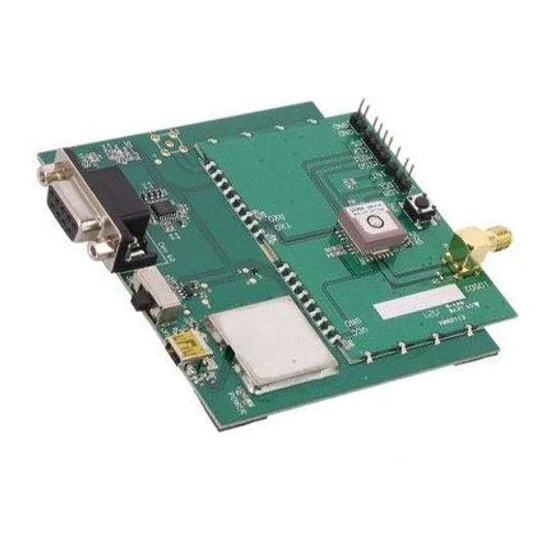
Summary of Contents for Sierra Wireless AirPrime XA1110
- Page 1 AirPrime XA1110 and XM1110 Hardware Design Guide 41111116 Rev 3.0...
- Page 2 Data may be delayed, corrupted (i.e., have errors) or be totally lost. Although significant delays or losses of data are rare when wireless devices such as the Sierra Wireless modem are used in a normal manner with a well-constructed network, the Sierra Wireless modem should not be used in...
- Page 3 This product may contain technology developed by or for Sierra Wireless Inc. This ® product includes technology licensed from QUALCOMM . This product is manufactured or sold by Sierra Wireless Inc. or its affiliates under one or more patents licensed from MMP Portfolio Licensing. Copyright © 2019 Sierra Wireless. All rights reserved.
-
Page 4: Table Of Contents
Contents Introduction ............6 Precautions. - Page 5 Contents UART to RS232 Interface ..........27 UART to USB Interface .
-
Page 6: Introduction
1: Introduction This document provides design guidelines for the following modules: • Stand Alone GNSS module XM1110 Figure 1-1: XM1110 Multi-GNSS Module • Integrated Patch Antenna Module: XA1110 Figure 1-2: XA1110 Precautions Please read carefully before you start If you use the GNSS receiver inside buildings, tunnels, or beside any huge objects, the GNSS signals might be cut-off or weakened. -
Page 7: General Rules For Design
2: General Rules for Design This section provides rules to obtain the best performance when using the GNSS module. Circuit Design Power Supply A clean and stable power supply is required for the GNSS modules to perform optimally. An unstable power source will significantly impact GNSS performance. To achieve high-quality performance, the VCC ripple must be controlled under 50mVpp. -
Page 8: Uart / I2C/ Spi Serial Interface
Hardware Design Guide If VBACKUP isn’t connected to any coin battery, the GNSS module will execute a cold start each time it’s restarted. Figure 2-2: Rechargeable coin battery with VBACKUP UART / I C/ SPI Serial Interface UART 0 (RX/TX) 1. -
Page 9: Antenna Compliance Design
General Rules for Design Figure 2-3: Addition of Pull-up Resistor SPI (CS/CLK/MISO/MOSI) 1. The serial peripheral interface port manages the communication between the digital BB and external devices. The MT3333 supports only slave mode. The slave has a 4 byte-register mode or URAM mode. In URAM mode, the size of the transmitted and received data is 256 bytes. - Page 10 Hardware Design Guide Designing an External Passive Patch Antenna with GNSS module 1. In general, a 50Ω patch antenna will work well with the GNSS module. The antenna can be connected to the Antenna IN pin with a 50Ω impedance trace.
- Page 11 General Rules for Design Table 2-1: Modes XM1110 XA1110 Mode 1 (via the VANT) (External Choke Coil) Mode 2 (from the VCC) (Internal Choke Coil) Figure 2-5: Mode 1 (External Choke Coil) Figure 2-6: Mode 2 (Internal Choke Coil) Rev 3.0 Aug.19 41111116...
- Page 12 Hardware Design Guide Designing a Chip Antenna with GNSS Module It’s recommended to consult chip antenna vendors for more specific design guidelines. Below references are for chip antennas from Pulse and Unictron. 1. Pulse Antenna Figure 2-7: Pulse Schematic Design Figure 2-8: Pulse PCB Layout Check antenna datasheet before tuning RF to match the component footprint (such as: C27, C28).
- Page 13 General Rules for Design Figure 2-9: Unictron Schematic Figure 2-10: Unictron PCB Check the antenna datasheet before tuning RF to match the component footprint (such as: C26, C27, C28, C29, C30). You can tune based on PCB size and housing to tune for an optimal value in order to meet the GNSS’s frequency and for good reception.
-
Page 14: 1Pps
Hardware Design Guide Table 2-2: GPS/GLONASS External Antenna (Continued) Characteristic Specification Power Supply 3.3V DC Current 5mA<IDC<11mA at 3.3V Total Gain 27±3dB Output VSWR Impendence 50Ω Noise Figure Table 2-3: Beidou/GPS External Antenna Characteristic Specification Polarization Right-hand circular polarized Frequency Received 1.561GHz~1.575GHz Power Supply 3.3V... - Page 15 Figure 2-11: 1PPS signal and its pulse width with 100ms duration Free run 1PPS Output Before 3D_FIX The Sierra Wireless standard GNSS module outputs 1PPS signal after the module obtains a 3D_FIX. This is a factory default setting. Cable Delay Compensation In some cases, a long-distance connection (~300m) may be needed.
-
Page 16: 1.8V Boost To 3.3V Application
Hardware Design Guide 1.8V Boost to 3.3V Application If you want to use the 3.3V’s GNSS module in a 1.8V system there are two considerations: power supply translation and signal level shift. For power supply translation, you can use a boost circuit which can boost 1.8V to 3.3V (refer to Figure 2-13 below). -
Page 17: Layout Guidelines
General Rules for Design For signal level shift, when your host system is 1.8V and the Sierra Wireless module is 3.3V, the host system can control the Sierra Wireless module by using a signal level shift circuit (refer to Figure 2-15 below). - Page 18 Hardware Design Guide Figure 2-16: GNSS Module with a Clean GND Plane Don’t place any trace such as I C (SCL/SDA), SPI (CLK/MISO/MOSI), UART (TX/ RX) underneath the GNSS module, otherwise it will cause a sensitivity decrease. For XA1110 To avoid the interference, place many vias on the two sides of the RF trace which goes from the module to the SMA/RF connector on your system PCB as illustrated in Figure 2-17...
-
Page 19: Keep Xa1110 Far Away From High Profile Or Metal-Canned Components
General Rules for Design Keep XA1110 Far Away from High Profile or Metal-Canned Components It’s good practice to place the GNSS module far away from any high-profile components especially those enclosed in metal cases such as the E-CAP, coin battery, and Pin Header. The antenna field pattern can be affected, and pattern distortion can occur. -
Page 20: Placement
Hardware Design Guide Figure 2-21: Example of Bad GPS Module Placement (Patch Antenna Close to a High-Profile Metal Case Component) and Good Placement Placement • Place the decoupling capacitors for the VCC close to the GNSS module. • Place the damping resistors for TX/RX close to GNSS module. Do not place the GNSS module: •... -
Page 21: Ground Segmentation
General Rules for Design Figure 2-23: Examples of Independent Trace Ground Segmentation In general, the separation of ground between the GPS module and the rest of the system is recommended to avoid interference. If this is not possible, it is best to follow these rules: segmentation of ground between digital and analogue system, high current and low current system, and different radiation systems such as GPS and GPRS. - Page 22 Hardware Design Guide Figure 2-24: Ground Plane for FR4 Design Rev 3.0 Aug.19 41111116...
-
Page 23: Thermal Profile For Smd Modules
3: Thermal Profile for SMD Modules The following information is Pb-Free compliant. The details are for reference only. SMT Reflow Soldering Temperature Profile • Solder paste alloy: SAC305 (Sn96.5/Ag3.0/Cu0.5). • Pre-heat Temp: 150–200°C; Soak time (ts): 60–120sec. Peak temp (Tp) ≤ 250°C. •... -
Page 24: Troubleshooting
4: Troubleshooting How to Check the Working Status of the GPS Module The first thing to check for is the NMEA sentence output through TX using various application tools. For example: you may use the Windows tool: HyperTerminal or you may use another GPS application program. -
Page 25: Super Capacitor Design
Appendix A: Super Capacitor Design About Super Capacitors Super capacitors have a lifetime similar to that of aluminum electrolytic capacitors. The service life of a super capacitor is greatly dependent on the operating temperature, humidity, applied voltage, current, and backup time. Therefore, the service life is determined based on the backup time set by the customer. -
Page 26: Ω Antenna Matching
Appendix B: 50 Ω Antenna Matching We used the AppCAD tool to simulate 50Ω impedance for the RF PCB layout. Table B-1: Antenna Matching RF Line Width (W) PCB FR4 Dielectric Copper Thickness Thickness Parameters per ounce 1.8mm 0.035mm Figure B-1: Dimensions Notice: For multi-layer layouts, you can place a ground layer in the second layer to minimize the trace width in a specific PCB (such as FR4) and impedance. -
Page 27: Uart To Rs232 Interface
Typically, an RS232 or USB interface is required to connect the PC to the Sierra Wireless GNSS module for communication. Most Sierra Wireless modules use a set of communication ports in TTL-logic. A bridge IC may be needed for RS232 signal conversion. -
Page 28: Uart To Usb Interface
Appendix D: UART to USB Interface If the Sierra Wireless module you have purchased does not come with a USB interface, it is possible to connect the module to an external USB IC. To further enhance the transferring speed, use one that is capable of USB version 2.0. Once the driver for the chosen USB Bridge IC is successfully installed onto Windows or another operating system, the USB Bridge IC will automatically be recognized as a COM port. -
Page 29: How To Efficiently Transfer 1Pps Through Extended Distances
1PPS. The accuracy level of 1PPS for Sierra Wireless GNSS modules is within 100ns. This applies to most of Sierra Wireless’ MTK GNSS modules. The reference design in... -
Page 30: 1Pps Delay Time
Hardware Design Guide 1pps Delay Time When using coaxial cable for long distance communication using an OP-amp for amplification, pay close attention to the coaxial cable time delay and the rising time of the wave form due to the OP-amp’s slew rate. A brief explanation for this is given below. -
Page 31: The Delay Time Caused By The Cable
How to Efficiently Transfer 1PPS Through Extended Distances The Delay Time Caused by the Cable Figure E-4: Delay Time Caused by the Cable Calculating the Delay Time in Respect to the Communication Cable Length The simplest method to calculate this is to have a good grasp of the relationship of the three parameters: 1. -
Page 32: Waveform Rising Time Caused By Op-Amp
Hardware Design Guide Other coaxial cable electromagnetic fundamental parameters along with the inner and outer diameter of the physical cable can be used in combination to perform theoretical calculations. Waveform Rising Time Caused by OP- Figure E-5 shows the slew rate which is the time needed for a rising waveform. μ... -
Page 33: Reflow Soldering Precautions
Appendix F: Reflow Soldering Precautions Table F-1: Precautions Details Suggestions Notes Before proceeding with Pre-bake Time: The maximum tolerated temperature for the reflow-soldering the tray is 100°C. 6 Hours @ 60°±5°C or process, the GPS 4 Hours @ 70°±5°C module must be pre- After the pre-baking process, please make baked. - Page 34 Hardware Design Guide Table F-1: Precautions Details Suggestions Notes Before handling the 1. You may use an electric It is very easy to cause a positional offset PCBA, they must be fan behind the reflow to the module and its patch antenna when cooled to 35°C or below machine to cool them down.
-
Page 35: Other Cautionary Notes On The Reflow-Soldering Process
8. If an SMT protection line is running a double-sided process for PCBA, please process the GPS module during the second pass only to avoid repeated reflow exposures of the GPS module. Please contact Sierra Wireless beforehand if you must process the GPS module during the first pass of double-side process. -
Page 36: Manual Soldering
Hardware Design Guide Manual Soldering Soldering Iron Heat Temperature: Under 380°C | Time: Under 3 sec. Notes: 1. To prevent further oxidation, do not directly touch the soldering pads on the surface of the PCB board. 2. The solder paste must be defrosted to room temperature before use so that it can return to its optimal working temperature.
Need help?
Do you have a question about the AirPrime XA1110 and is the answer not in the manual?
Questions and answers