Table of Contents
Advertisement
Quick Links
Advertisement
Table of Contents

Subscribe to Our Youtube Channel
Related Manuals for Humandata XP68-03 Series


Summary of Contents for Humandata XP68-03 Series
- Page 1 PLCC68 Spartan-6 FPGA Module XP68-03-LX45 User’s Manual Ver. 1.0 HuMANDATA LTD.
-
Page 2: Table Of Contents
Table of Contents Revision History ....................1 Introduction ....................1 1. Specifications ..................... 2 2. Overview ......................3 2.1. Name of Parts .......................3 2.2. Pin Assignment ....................4 2.3. Power Supply ......................5 2.4. Clock ........................5 2.5. Configuration Switch (SW1) ................5 3. - Page 3 HuMANDATA will revise the diagram. When a problem can be solved only by replacing components or modifying the product, HuMANDATA will take back the product to replace it with a properly functioning product.
-
Page 4: Revision History
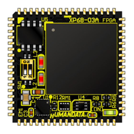
Revision History Date Revision Description Jan. 26, 2012 v1.0 Initial release Introduction Thank you for purchasing our product XP68-03-LX45, PLCC68 Spartan-6 FPGA Module. This is an FPGA Module equipped with a XILINX FPGA Spartan-6, voltage regulators, oscillators and configuration device. XP68-03 can be equipped on 2.54mm pitch universal boards by using a 68pin through hole PLCC socket. -
Page 5: Specifications
1. Specifications Model Name XP68-03-LX45 XC6SLX45-2CSG324C FPGA Config. Device M25P16-VMN6 (Numonyx, 16Mbit) User I/Os I/O Banks 2 groups (VIOA, VIOB) On-Board Clock 50 [MHz] External Clock Input 4 (shared with user I/O) User Switch 1 (Slide) User LEDs Power Input DC 3.3 [V] I/O Power Input 1.2 [V] to 3.3 [V] (please refer to FPGA datasheet) -
Page 6: Overview
2. Overview 2.1. Name of Parts Config. Device Config. SW User SW FPGA User LEDs DONE LED Component Side Spacer x4 Oscillator 50MHz Solder Side XP68-03-LX45 v1.0... -
Page 7: Pin Assignment
2.2. Pin Assignment TOP VIEW XP68-03-LX45 v1.0... -
Page 8: Power Supply
2.3. Power Supply This module operates from single DC 3.3 V power supply from 35pin and 36pin. Internally required 1.2[V] are generated by an on-board voltage regulator. The external power supply should be sufficient and stabilized. Please do not apply over 3.3V voltage. -
Page 9: Jtag Connection
3. JTAG connection JTAG signal is led out to pins as below. Please prepare an external connector to access to the FPGA and the configuration device. JTAG buffer or other process is needed as the situation demands. When those pins are unused, please connect them to GND and do not leave them open. If consumption current caused by on-board pull-up or pull-down resistors would be a problem, connect the signals to GND or V33P according to the circuit design. -
Page 10: Configuration Device Programming
5. Configuration Device Programming An mcs file is required to download an FPGA configuration data to the configuration device via JTAG. To generate an mcs file using iMPACT, please refer to the following steps. 5.1. Generating mcs file Start iMPACT, and double-click [Create PROM File] and set items as shown below. -
Page 11: Plcc Socket
6. PLCC socket This module is designed to be used with 68pin PLCC socket, and 4 spacers are mounted on reverse side. These spacers or other components might be obstacle to spacers on some PLCC socket. Please be careful when selecting PLCC socket. Proper mounting and operation with following PLCC sockets is confirmed. - Page 12 PLCC68 Spartan-6 FPGA Module XP68-03-LX45 User’s Manual Ver. 1.0 ..........Jan. 26, 2012 HuMANDATA LTD. Address: 1-2-10-2F, Nakahozumi, Ibaraki Osaka, Japan ZIP 567-0034 Tel: 81-72-620-2002 (Japanese) Fax: 81-72-620-2003 (Japanese/English) URL: http://www.hdl.co.jp/en/ (Global) http://www.hdl.co.jp/ (Japan)
Need help?
Do you have a question about the XP68-03 Series and is the answer not in the manual?
Questions and answers